IEEE ELECTRON DEVICE LETTERS, VOL. 22, NO. 10, OCTOBER 2001 475
Enhanced Degradation in Polycrystalline
Silicon Thin-Film Transistors Under
Dynamic Hot-Carrier Stress
Kow Ming Chang, Yuan Hung Chung, Gin Ming Lin, Chi Gun Deng, and Jian Hong Lin
Abstract—We address the mechanisms responsible for the enhanced degradation in the polysilicon thin-film transistors under dynamic hot-carrier stress. Unlike the monotonic decrease of maximum transconductance ( m max) in static stress, m max in dynamic stress is initially increased due to the channel short-ening effect by holes injected into the gate oxide near the drain region and then decreased due to tail states generation at the gate oxide/channel interface and grain boundaries. The threshold voltage variations are dominated by two degradation mechanisms: 1) breaking of weak bonds and 2) breaking of strong bonds to obey the power-time dependence law with a slope of 0.4. The degradation of the sub-threshold slope is attributed to intra-grain bulk states generation.
Index Terms—Channel shortening effect, intra-grain bulk states, polysilicon thin-film transistors (poly-Si TFTs), tail states, transconductance ( m max).
I. INTRODUCTION
P
OLYSILICON thin-film transistors (poly-Si TFTs) have received increasing attention for application in active ma-trix liquid crystal displays (AMLCDs) and static random-ac-cess memories (SRAMs). Reliability is one of the major con-cerns, especially when a device is operated under high drain and high gate voltages. Hot carrier stress under high drain and high gate voltages decreases the transconductance, turn-on current, sub-threshold slope and increases the threshold voltage [1], [2]. Although the study of device aging with stress time under static hot-carrier stress has been systematically reported [3], to our knowledge, a study of the degradation in poly-Si TFT perfor-mance under dynamic hot-carrier stress has not been reported. Moreover, dynamic stress is closer to real operational condi-tions than static stress [4]. In this letter, we study the degradation mechanism by analyzing the evolution of device parameters in-cluding transconductance, threshold voltage, and sub-threshold slope.II. EXPERIMENT
First, an undoped 100-nm-thick amorphous Si film was de-posited on 500-nm-thick thermal oxide by decomposition of
Manuscript received June 7, 2001; revised July 27, 2001. This work was supported by the National Science Council of Taiwan, R.O.C., under Contract NSC89-2215-E009-089. The review of this letter was arranged by Editor T.-J. King.
The authors are with the Department of Electronics Engineering and Insti-tute of Electronics of National Chiao-Tung University, Hsinchu, Taiwan, R.O.C. (e-mail: [email protected]).
Publisher Item Identifier S 0741-3106(01)08863-2.
Si H at 460 C in a low-pressure chemical vapor deposition system and then crystallized at 600 C for 24 h. The measured average grain size is 1.1 m. After defining the active channel region, a 50-nm-thick plasma–enhanced chemical vapor depo-sition SiO film was deposited at 350 C to serve as the gate dielectric. A 300-nm-thick amorphous Si gate layer was then deposited and patterned. Source and drain regions were formed by ion implantation of P cm KeV and then activated at 600 C for 12 h. Finally, passivation oxide and metal layers were deposited and patterned. Channel length and width are 10 m and 5 m, respectively. No hydrogenation step was performed on the poly-Si TFTs.
For dynamic stress, the drain is biased at V and the gate bias is square waveform switching from 0 V to 20 V with rise time 100 ns, fall time 100 ns and duty cycle 50%. For static stress, V and V were used. Threshold voltage is extracted by extrapolation of the curve from the point of in the linear regime ( V).
III. RESULTS ANDDISCUSSION
Fig. 1(a) and (b) show the different degradation behaviors of drain current and transconductance under static and dynamic stress, respectively. For static stress, decreases mono-tonically with the increase of the stress time at in the range of V V and remains unchanged for V. For dy-namic stress, the curve of the transconductance shows a parallel shift in the positive direction, while is initially increased and then it starts to decrease after 1000 s stressing.
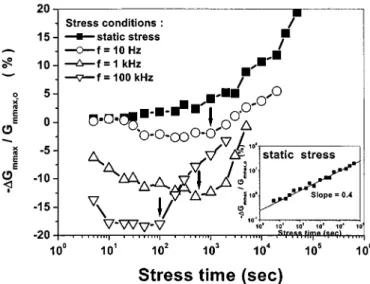
Fig. 2 shows the degradation of the defined as , where
, is the initial and is the for each stress time. For dynamic stress,
initially increases, then saturates and finally starts to decrease after the turnaround point (as indicated by the arrow in Fig. 2). rising is attributed to channel shortening effect by holes injected into the gate oxide region near drain [5]. In the ON state, impact ionization will occur to generate hot electrons and hot holes near the drain. Once the device is switched from ON state to OFF state, the channel electrons will be repelled quickly into the drain side to gain additional energy and cause serious impact ionization near the drain. During the OFF state stress period, the electric field near the drain is very suitable ( V) for holes injecting into the gate oxide. When the injected holes reach saturation at the turnaround point, tail states generation in the grain boundaries and gate
476 IEEE ELECTRON DEVICE LETTERS, VOL. 22, NO. 10, OCTOBER 2001
(a)
(b)
Fig. 1. Degradation of drain current and trans-conductance by (a) static stress and (b) dynamic stress.
Fig. 2. Degradation of maximum trans-conductance as a function of the stress time under static and dynamic stress.
oxide/channel interface start to dominate degradation [3]. As the stress frequency increases, hole concentration will increase [6] and cause more serious channel shortening effect. However, for static stress, decreases monotonically and the insert plot of Fig. 2 shows that degradation
Fig. 3. Threshold voltage variations as a function of stress time under static and dynamic stress.
Fig. 4. Subthreshold slope variations as a function of stress time under static and dynamic stress.
exhibits a power-time dependence with a slope of 0.4 which is due to the tail states generation in the grain boundaries and at the gate oxide/channel interface [3], [7].
Fig. 3 shows the threshold voltage variations th after stressing. Clearly, th for static stress exhibits a power-time dependence with a slope of 0.4 and is much smaller than that of dynamic stress. For the dynamic stress, th first saturates (first stage) and then it shows a power-time dependent law with a slope of 0.4 (second stage). The degradation in the first stage is due to deep states generation in the grain boundaries and at the gate oxide/channel interface by breaking the weak Si-H and Si-Si bonds. Once all of the available weak bonds are broken, th saturates. The additional increase in th after the turnaround point indicated by the arrows in Fig. 3 is due to the strong Si-Si bonds breaking [7], [8].
Fig. 4 shows the evolution of the sub-threshold slope varia-tion , where , is the initial sub-threshold slope and is the sub-threshold slope for each stress time. A power-time dependence with a slope of 0.18~0.25 is
CHANG et al.: ENHANCED DEGRADATION IN POLYCRYSTALLINE SILICON 477
observed for both static and dynamic stress. Unlike in laser-an-nealed poly-Si TFTs where the sub-threshold slope remains un-changed after stressing [3], in solid-phase crystallized poly-Si TFTs, the sub-threshold slope varies with stress time indicating that intra-grain bulk states are generated in the poly-Si film [9]. Because the poly-Si film was formed by solid-phase crystalliza-tion method in this letter, intra-grain bulk state density is much higher and Si-Si bonds are weaker than those in laser-crystal-lized poly-Si film. Some more detailed study of the fall time and stress temperature effects on the device degradation is in progress.
IV. CONCLUSION
Poly-Si TFT degradation mechanisms under dynamic hot-carrier stress were studied. rising is due to channel shortening effect by hole injection into the gate oxide near the drain. As the stress frequency increases, the degradation becomes more serious. th is dominated by two degradation mechanisms: breaking of weak bonds initially and breaking of strong bonds to obey a power-time dependence law in the second stage. The degradation of the sub-threshold slope is attributed to intra-grain bulk states generation in the poly-Si film.
REFERENCES
[1] M. Hack, A. G. Lewis, and I. W. Wu, “Physical models for degradation effects in polysilicon thin-film transistors,” IEEE Trans. Electron
De-vices, vol. 40, pp. 890–897, May 1993.
[2] F. V. Farmakis, C. A. Dimitriadis, J. Brini, G. Kamarinos, V. K. Gue-orguiev, and Tz. E. Ivanov, “Interface state generation during electric stress in n-channel undoped hydrogenated polysilicon thin-film transis-tors,” Electron Lett., vol. 34, no. 24, pp. 2356–2357, 1998.
[3] F. V. Farmakis, J. Brini, G. Kamarinos, and C. A. Dimitriadis, “Anoma-lous turn-on voltage degradation during hot-carrier stress in polycrys-talline silicon thin-film transistors,” IEEE Electron Device Lett., vol. 22, pp. 74–76, Feb. 2001.
[4] Y. Uraoka, T. Hatayama, and T. Fuyuki, “Reliability evaluation method of low temperature poly-silicon TFT’s using dynamic stress,” in Proc.
of the 2000 Int. Conf. on Microelectronic Test Structures, 2000, pp.
158–162.
[5] F. V. Farmakis, J. Brini, G. Kamarinos, C. A. Dimitriadis, V. K. Gue-orguiev, and Tz. E. Ivanov, “Electrical stress in N- and P- channel un-doped-hydrogenated plolysilicon thin film transistors (TFT’s),” in Int.
Semiconductor Conf. CAS ’99 Proc., vol. 1, 1999, pp. 157–160.
[6] A. G. Lewis, I. W. Wu, M. Hack, A. Chiang, and R. H. Bruce, “Degra-dation of polysilicon TFT’s during dynamic stress,” in in IEDM Tech.
Dig., 1991, pp. 575–578.
[7] G. A. Armstrong, S. Uppal, S. D. Brotherton, and J. R. Ayres, “Differ-entiation of effects due to grain boundary traps in laser annealed poly-Si thin film transistors,” Jpn. J. Appl. Phys., vol. 37, pp. 1271–1276, 1998. [8] F. V. Farmakis, J. Brini, G. Kamarinos, C. T. Angelis, C. A. Dimitriadis, M. Miyasaka, and T. Ouisse, “Grain and grain-boundary control of the transfer characteristics of large-grain polycrystalline silicon thin-film transistors,” Solid-State Electron, vol. 44, pp. 913–916, 2000. [9] G. A. Armstrong, S. Uppal, S. D. Brotherton, and J. R. Ayres,
“Mod-eling of laser-annealed polysilicon TFT characteristics,” IEEE Electron