High brightness ⅢⅢⅢⅢ-ⅤⅤⅤⅤ light-emitting diodes on diamond/silicon composite substrate
Tai-min Chang, Jen-Li Hu, Bo-Wen Lin, YewChung Sermon Wu
Department of Materials Science and Engineering, National Chiao Tung University, Hsinchu 30010, Taiwan, R.O.C.
Thermal management of LED is currently an important issue because the increase of junction temperature degrades LED’s performance and reliability. Replace that substrate to high thermal conductivity substrate can improved this problem. Diamond has the highest thermal conductivity (~2000W/mK) in all material but is hard to process and has low reactivity with other material. In this study, high-brightness Ш-Ѵ light-emitting diodes on Si/diamond composite substrate can be fabricate by filled diamond particle into the blind-hole of the silicon substrate, wafer-bonding and lift-off process. In order to confirm that diamond particle provided a direct thermal path for heat dissipation, a simple sandwich structure was also been done.
Introduction
light-emitting diodes have the great potential to be the next-generation light source due to their high-brightness and long lift-time [1]. Thermal management of LED will be very important because the increase of junction temperature degrade LED’s performance and reliability. Replace that substrate to high thermal conductivity substrate can improved this problem [2][3].
Diamond has the highest thermal conductivity (~2000W/mK) in all material. Many researches tried to using diamond as heat dissipation material to improve LED’s performance. The methods include deposited CVD-diamond thin film [3]. But high quality diamond film can only deposited few dozens of micron-meter thick, and the deposited process was also too complicated and time-consuming. Another method is fabricated diamond/metal or diamond/polymer composite material [4][5]. But because of the low reactivity nature of diamond, the process usually involved high temperature and high pressure procedure that was not suitable for manufacture LEDs. Recently, Horng et
al.[6] demonstrated improved LEDs performance by employing diamond-add solder as a
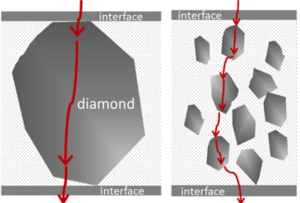
die attach material. But according to the low reactivity nature of diamond, too much interface between diamond and solder would hinder heat pass through the entire structure. In this study, we made a high thermal conduct diamond/silicon composite substrate by filled diamond particle into the blind-hole of the silicon substrate. Not only provide a simple way to fabricated high thermal conduct substrate with diamond but also decrease the effect of interface that hinder heat pass through diamond-add materials. The schematic diagram of different heat pass between diamonds-add solder and our study was shown in Fig. 1. Then by wafer-bonding and lit-off process [7], high-brightness Ш-Ѵ light-emitting diodes on Si/diamond composite substrate can be fabricate
Fig. 1 The schematic diagram of different heat pass between our study(left) and diamonds-add solder(right). Red arrows represent the heat route.
Experiment
First, a 2µm-thick SiO2 layer was deposited and patterned on Si substrate act
as etching mask. Then, a 200µm depth blind-hole with octagonal column shape was fabricated by using Inductive-Couple Plasma (ICP) etching. Artificial diamond particle with size ~200µm was filled into the octagonal column by using Benzocyclobutene (BCB) as adhesion material. 100nm Ti and 2µm thick Cu metallization layer was deposited on the silicon/diamond composite substrate after diamond filing process. The metallization of LED chip was ITO (indium-tin oxide) and Cu layer, ITO act as current spreading layer and Cu is wetting layer. By wafer-bonding and lit-off process, GaN LED on silicon/diamond composite substrate can be fabricated. First, SAC309 solder was apply to the middle between LED chip surface and silicon/diamond composite substrate. The
reflow was proceeding on hot-plate with some pressure, the temperature was set at 250°C and time was 5 min. The SAC309 solder not only served as bonding material but also moderate thermal stress between sapphire and silicon/diamond substrate during lit-off process. Then by lit-off process, the sapphire will be successfully separate from GaN-epi layer.
Result and discussion
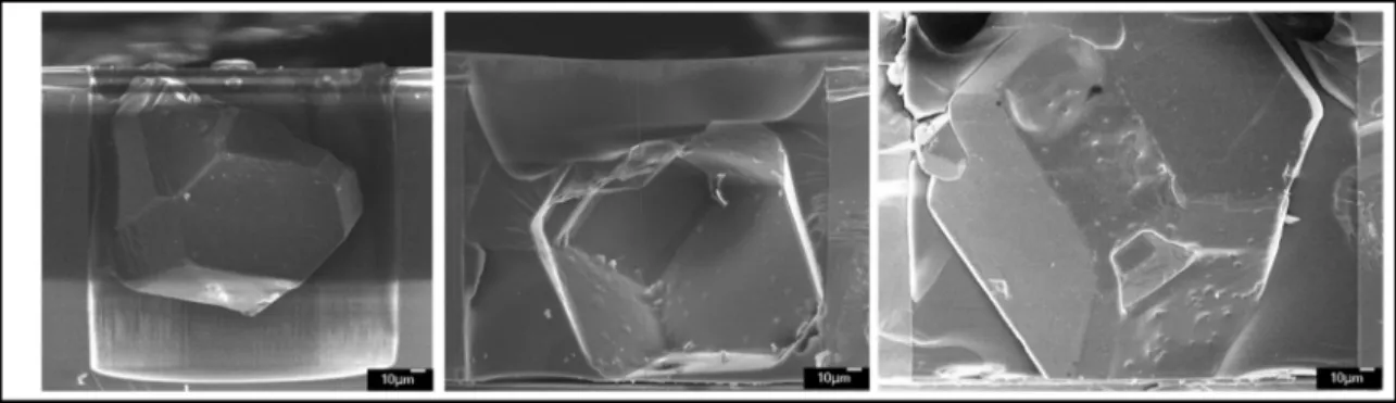
Fig. 2 shows the SEM image of silicon blind-hole filled with artificial diamond particle with different condition. Note that the size of artificial diamond particle was not so accurate, so the filling condition would different due to the size variation. The best condition would be that diamond particle slightly contact to the GaN-epi layer by SAC309 solder. Filling condition with smaller diamond particle would generate thicker solder interface or gap between GaN-epi layer and silicon/diamond composite substrate, will reduce the advantage of high thermal conductivity benefit from the diamond particle.
Fig. 2 SEM image of silicon blind-hole filled with artificial diamond particle with different condition
In order to confirm that silicon/diamond composite substrate in our study provided a direct thermal path for heat dissipation, we use a simple sandwich structure to reduce the complexity. The sandwich structure includes a single layer of diamond particle package with SAC309 solder grip by a pairs of silicon substrate. The size of artificial diamond particle use here was ~30μm, so the thickness of diamond/solder middle layer was 30μm thick. Fig. 3a shows the SEM image of the sandwich structure. For comparison, a pair of silicon substrate bonded with 30μm thick SAC309 solder also prepared. Fig. 3b shows that when heat flow through the sandwich structure will pass through the sequence of silicon substrate / interface / diamond and solder / interface / silicon substrate and silicon substrate / interface / solder / interface / silicon substrate. Compare thermal resistance between those two different sample, we can calculated how much promotion of thermal dissipation was contribute by diamond particle.
Fig. 3 (a) The schematic diagram of heat flow through the sandwich structure (b)
Conclusion
High-brightness Ш-Ѵ light-emitting diodes on Si/diamond composite substrate can be fabricate by filled diamond particle into the blind-hole of the silicon substrate,
wafer-bonding and lit-off process. The structure not only provide a simple way to fabricated high thermal conduct substrate with diamond but also decrease the effect of interface that hinder heat pass through diamond-add composite materials. In order to confirm that silicon/diamond composite substrate in our study provided a direct thermal path for heat dissipation, we use a simple sandwich structure to reduce the complexity. Compare thermal resistance between two different sandwich sample, we can calculated how much promotion of thermal dissipation was contribute by diamond particle.
Acknowledgments
This project was funded by Sino American Silicon Products Incorporation and the National Science Council of the Republic of China under Grant No. 98-2221-E009-041-MY3. Technical supports from the National Nano Device Laboratory, Center for Nano Science and Technology, Nano Facility Center and Semiconductor Laser Technology Laboratory of the National Chiao Tung University are also acknowledged.
References
1. C. F. Chu, C. C. Cheng, W. H. Liu, J. Y. Chu, F. H. Fan, H. C. Cheng, T. Doan, and C. A. Tran, Proceedings of the IEEE, 98, 1197 (2010)
2. Wei Chih Peng and YewChung Sermon Wu, Appl. Phys. Lett., 84, 1841 (2002). 3. Po Han Chen, Ching Liang Lin, Y. K. Liu, Te Yuan Chung, and Cheng-Yi Liu,
IEEE Photon. Technol. Lett., 20, 845 (2008).
4. Andrey M. Abyzov, Sergey V. Kidalov, Fedor M. Shakhov, J Mater Sci, 46, 1424 (2011)
5. A. Gracias, N. Tokranova, B. C. M. Thelen, J. Castracane, Physica Status Solidi (a)
208, 684 (2011)
6. C. J. Chen, C. M. Chen, R. H. Horng, D. S. Wuu, J. S. Hong, J. Electronic Materials,
39, 2618 (2010)
7. W. S. Wong, T. Sands, N. W. Cheung, M. Kneissl, D. P. Bour, P. Mei, L. T.Romano, and N. M. Johnson, Appl. Phys. Lett., 75, 1360 (1999).