國 立 交 通 大 學
顯 示 科 技 研 究 所
碩士論文
奈米圖形化玻璃基板應用於非晶矽薄膜太陽能電池
Patterned glass substrates for enhanced solar energy
harvesting in thin film solar cells
研究生:蔡育霖
指導教授:郭浩中 教授
2
奈米圖形化玻璃基板應用於非晶矽薄膜太陽能電池
Patterned glass substrates for enhanced solar energy harvesting
in thin film solar cells
研究生:蔡育霖 Student:Yu-Lin Tsai
指導教授:郭浩中 教授 Advisor:Hao-Chung Kuo
國 立 交 通 大 學
顯 示 科 技 研 究 所
碩 士 論 文
A Thesis
Submitted to Display Institute
College of Electrical Engineering
National Chiao Tung University
in Partial Fulfillment of the Requirements
for the Degree of
Master
In
Display
July 2011
Hsinchu, Taiwan, Republic of China
i
奈米圖形化玻璃基板應用於非晶矽薄膜太陽能電池
研究生:蔡育霖 指導教授:郭浩中 教授
國立交通大學顯示科技研究所
摘要
本論文中,我們針對矽薄膜太陽能電池主動層厚度不足,導致太陽光能量吸收 效率不佳的問題來進行改良,其中特別改善長波長範圍太陽光之吸收效率,並增 進矽薄膜太陽能電池之光電轉換效率。 玻璃基板經常被使用作為矽薄膜沉積之基板,我們利用聚苯乙烯微奈米小球自 聚集之特性,成功地將聚苯乙烯微奈米小球鋪排在玻璃基板上,並形成單層六方 最密堆積的週期性結構,在此研究中我們利用微奈米球微影技術直接將大面積奈 米結構製作於玻璃基板上,並可利用乾式非等向性反應式離子蝕刻參數的調整, 得到不同形貌的次波長結構,並得到不同的抗反射與散射效果。 本篇論文第一部分討論如何在玻璃基板上製作次波長抗反射結構。首先我們以 濕蝕刻製程利用氧化物緩衝蝕刻液來蝕刻玻璃基板,但在實驗中我們發現,以氧 化物緩衝蝕刻液來蝕刻玻璃基板時的側向蝕刻速率,遠高於縱向蝕刻率,我們並 無法得到深寬比足夠的奈米結構,因此我們認為濕蝕刻並不適合用來製作奈米結 構玻璃基板。因此我們轉向利用旋塗法在玻璃基板上製作周期性的單層聚苯乙烯 小球周期性排列,此方法成本低廉又快速,更進一步我們成功利用乾式非等向性 反應式離子蝕刻技術在玻璃基板上製作出仿生結構。第二部分,我們將此種具有 仿生結構之玻璃基板應用於非晶矽薄膜太陽能電池上,並針對元件之反射率、外 部量子效應、光電轉換效率等來進行分析,並以變角度反射率量測來證明次波長ii 結構在變角度下仍然有不錯的抗反射效果,因此我們觀察到全波段量子效率的提 升,將此具有仿生結構之玻璃基板基板應用於非晶矽薄膜太陽能電池上,相較於 使用沒有製作仿生結構之平面玻璃基板太陽能電池元件,提高了 51.6%光電流增 加與光電轉換效率 48.4%的增強,相較於常被用於業界具有微米結構的 Asahi-U 基板元件,也提升了 8%的光電流,與 3.1%光電轉換效率,有效驗證了仿生結構 玻璃基板對於非晶矽薄膜太陽能電池光電轉換效率之提昇是有幫助的。 其中我們也利用 RCWA 模擬將仿生結構的周期與高度作最佳化的分析,於實際 元件製作中我們發現,受制於非晶矽薄膜之厚度過薄,高度過高的仿生結構將導 致薄膜覆蓋不均勻,影響元件電性之表現,因此光學最佳化之結構並不一定能得 到最佳的光電轉換效率,在太陽能電池元件電性與仿生結構高寬比的分析中,我 們認為在考慮電特性的情況下, 最佳的玻璃基板奈米結構深寬比大約界於 0.2~0.3 之間,這樣的深寬比選擇讓我們在光學特性與電特性中找到平衡,雖然 我們最後所採用之結構並非光學最佳化之結構,但我們仍然觀察到使用仿生結構 玻璃基板的非晶矽薄膜太陽能電池有全波段的外部量子效率提升,與光電轉換效 率的提升。 最後我們相信如果我們能解決因過大的奈米結構深寬比,而導致薄膜覆蓋不均 勻並導致元件電性下降的問題,仿生結構玻璃基板必定能提升更多的太陽能電池 轉換效率。
iii
Patterned glass substrates for enhanced solar energy harvesting in
thin film solar cells
Student:Yu-Lin Tsai Advisor:Hao-Chung Kuo
Display Institute
National Chiao Tung University
Abstract
The amorphous silicon (a-Si) thin film solar cell was considered for future generation of photovoltaic applications due to the low cost. However, due to the thin active layer (<1um), it shows a low absorption coefficient at near-infrared region. How to improve light harvesting is a very important issue in high efficiency a-Si thin film solar cell. Antireflection and light trapping are key techniques for efficiently harvesting solar photon. Several studies of sub-micrometer gratings (SMG) structure demonstrate the SMG structure offer a graded refraction index interface, and shown ultra-low reflectivity, another feature of SMG structure is diffraction of light, which get longer optical path length and then further enhance the light absorption of a-Si thin film.
In this work, the enhanced conversion efficiency is demonstrated in nanostructured glass substrate for a-Si thin film solar cell, and the nanostructured glass substrate was fabricated by using nanosphere lithography and RIE techniques. The measured external quantum efficiency shows a broadband light absorption, which specially enhance the light absorption in near-infrared. The nanostructured substrate provided both antireflective characteristic and light scattering characteristic for improving the solar energy harvesting. From the result of the I-V characteristics, we observe the electrical property will decrease when the H/D ratio of biomimetic
iv
structures increase. We believe that higher H/D ratio of biomimetic structure will result in uneven coverage of thin film growth. From the experiment result, we conclude the best H/D ratio for biomimetic glass structure applies in a-Si thin film solar cell is around 0.2~0.3.
Finally we demonstrated the biomimetic glass substrate (nipple shape arrays) which is useful in harvesting solar photon and enhancing the power conversion efficiency of a-Si thin film solar cell. Compared with a flat glass substrate cell and Asahi-U glass substrate cell, the power conversion efficiency achieved 48.4% and 3.1% enhancement, and the Jsc achieved 51.6% and 8% enhancement respectively.
v
Acknowledgements
時光飛逝,想起兩年前自己還只是個大學生,如今卻已經碩士畢業了。首先 我要感謝我的指導老師郭浩中教授,平時的鼓勵以及對於我實驗上的支援,讓我 可以無後顧之憂地進行實驗。另外也感謝余沛慈教授、林建中教授、賴芳儀教授 在我論文上的指教,使我的論文能更臻完整。 這兩年來感謝所有幫助過我的學長姊,清華學長感謝你在我剛進實驗室時領導 著我該如何進行自己的實驗。阿菲學長感謝你把你所有製程上的技巧傳授給我, 讓我受益良多,也很懷念以前在奈米中心與你一起跑製程,哈拉打屁的日子。Gibu 學長,很開心可以跟你一起合作這篇論文,你總是很有衝勁的帶著我向前衝,常 常提出一些我沒有想過的方法,才能讓這篇論文有不錯的結果,真的非常謝謝你, 希望你在剩下的博士生涯,能過得開心快樂一些。這兩年來最最最感謝的學長就 是閔安學長,感謝你帶著我從完全不懂太陽能電池,到能完成這篇論文,從你身 上學到的不只是專業知識的部分,更讓我學到處理事情的態度,真的非常謝謝你。 Solar team 的麥可、信助、珣彣、祐廣,和你們一起做研究真的很愉快,也謝 謝你們平常的照顧。Joseph、家華、板弟、鏡學、主立、柏孝、阿伯、David、 小見,謝謝你們總是不厭其煩的在製程上的幫忙,或是與我討論我的實驗,帶給 我很大的幫助。祝福所有學長姐工作的工作順利,念書的 paper 發不完,早日拿 到博士學位。
畢業後最讓我不捨的就是實驗室同屆的同學,有你們在,讓我原先覺得苦悶 的碩士生活變得開心又充實,看著大家一起出遊的照片,想起我們的一起踏過的 足跡,就覺得好開心,也好不捨。實驗室一姐羿蓁,就像我說的你有一種無形的 力量可以把我們大家拉在一起,所以感謝你勾引了大家,把我們大家串聯起來, 每次出遊也總是麻煩你處理了一堆事情,真的非常謝謝你,平常有時愛開你的玩 笑也請你見諒了。瑋婷,很懷念你平時傻傻又單純的笑容,希望你能一直保持下
vi 去,也祝福你工作順利。NDL 一姐 KaKa,每次都被你慢半拍的行為弄到快笑死, 西雅圖、溫哥華之旅更見識到你慢半拍的功力,也感謝你每次我們發起甚麼活動, 你總是義不容辭地參加。季瑾,雖然你平時因為實驗的關係,不常與我們一起活 動,但非常感謝你總是很認真地聽我哈拉,祝福你往後的工作一切順利。肉哥, 感謝你時常帶我們在新竹尋找美食,也很開心可以跟你一起在 solar team 裡學 習,從你身上我也學到了不少,未來還要一起繼續努力,但我還是希望你可以跟 我們去好樂迪。祐慶,很喜歡跟你邊在麵攤吃東西邊聊天的感覺,一起發洩的感 覺真的很不錯,對於有時看到你因為實驗上的挫折而心情不好,我卻不太能幫忙 你甚麼,感到有些抱歉,但很開心的是最後你還是順利畢業了,未來工作加油了。 大寶,一直覺得你是個很妙的人,懂得事情也很多,也很懷念跟你還有幼齒凌晨 跑去吃消夜,哈拉的日子,非常謝謝你總是為大家默默的付出,也祝福你以後能 過你最想過的奢華生活。PO 哥,我只能說你是神,平時總是搞不清楚狀況,但 還可以跟團跟的很開心,你總是給我一種很單純很有傻勁的感覺,常常讓我覺得 有些事情我們不要想的太多,只要朝自己設定的目標前進就好了,跟你相處在一 起真的會讓人心情變好,祝福你的未來一切順利。小杜,謝謝你在實驗上的幫忙, 就算你離我們很遠,但每次聚會你總是會出現,謝謝你平常總是負責調酒給大家 喝,也祝福你能順利出國去。祐國,你是個很厲害卻又很謙虛的人,真的是能玩 又能念書,看著你處理事情的態度,讓我覺得我還有好多需要努力,也謝謝你平 時常常與我討論實驗的問題,祝福你出國一切順利,有空要常回來拚酒阿。家齊, 還記得在實驗室搬家的時候,跟你越來越熟,雖然你年紀比我小很多,但總覺得 在處理事情方面你是很成熟的,也祝福你轉行成功。Just,感謝你之前在高雄帶 領大家到很多好玩的地方玩,接下來博班的日子也要一起好好努力了。SGG,你 真的是個新竹通,在新竹要去哪裡找你準沒錯,謝謝你平常的幫忙,祝福你未來 一切順利。峰瑜,非常懷念一起打 RIE 哈拉的日子,也非常謝謝你肯花時間跟我 一起討論製程上的問題,一起解決小球排列的問題,你樂心助人的一面讓我印象
vii 深刻,祝你未來在台 GG 的生活一切順利,賺大錢。冠霖,感謝你平常的幫忙, 每次在軟體上有甚麼問題找你好像都一定有解,有空再一起回來喝一杯,祝福你 研替生活一切順利,股票賺很大。大頭,雖然你後來就到了 NDL 做實驗,但還是 很懷念跟你互叫帥哥的日子,你迷人的笑容總是像陽光一般感染到我,謝謝你平 時經常借我攝影器材了,祝福你一切順利,愛你所選。13、懷翔、萬海、小蔡, 也感謝你們平時的幫忙,祝你們都能順利畢業。 我要感謝 mei,謝謝你一直從大學以來對我的包容,也謝謝你總是在我抱怨的 時候,當一個忠實的聽者,也祝福你能夠早日考上高考,朝我們一起擬定的目標 邁進。最後我要感謝我的家人,從小到大你們總是我最有力後盾,讓我能無後顧 之憂的求學,我也會繼續努力向上,期許自己能不讓你們失望,也希望未來我能 加倍的回饋你們,也祝福你們能永遠健康快樂,我愛你們。 蔡育霖 2011.08 於交通大學
viii
Content
摘要... i Abstract ... iii Acknowledgements ...v Content ... viii List of Tables ...x List of Figures ... xiChapter1. Introduction ...
11.1 Brief development of the solar cell...2
1.2 The advantages and the challenge of thin-film solar cells...5
1.3 Motivation...6
Chapter2. The physics of solar cells and brief introduction of
amorphous silicon
2.1 The fundamental structure of solar cell ...72.2 The physics of solar cells ...9
2.3 The parameter of solar cells ... 11
2.4 Brief introduction of amorphous silicon 2.4.1 Brief history of amorphous silicon ...13
2.4.2 The characteristics of amorphous silicon thin film ...14
Chapter3. Experimental Instruments and Methods
3.1 Scanning Electron Microsope (SEM) ...183.2 Transmission electron microscope (TEM) ...19
3.3 Angle resolved Integrating sphere reflectance measurements ...20
3.4 Current-voltage measurement (J-V curve) ...22
ix
Chapter4. The review of nanostructure fabrication
4.1 Photolithography ...28
4.2 E-beam lithography ...28
4.3 Nanoimprint lithography ...30
4.4 Nanosphere Lithography (NSL) ...33
Chapter5. Device fabrication and characteristics analysis
………...375.1 The fabrication of nanostructed glass substrate by using wet etching process ...38
5.2 The fabrication of nanostructed glass substrate ...40
5.2.1 The fabrication of monolayer and hexagonal nanosphere arrangement...40
5.2.2 The fabrication of nanostructed glass substrate by using anisotropic reactive ion etching technology………..….44
5.3 The fabrication of patterned glass substrate a-Si thin film solar cell ...47
5.4 The simulation of optical characteristic………..51
5.5 The reflectance of biomimetic glass substrates a-Si solar cells…………..……52
5.6 Angular reflectivity……….54
5.7 The current-voltage (I–V) characteristics………56
5.8 External quantum efficiency………..……….58
5.9 The effect of H/D ratio………....59
Chapter 6. Conclusion
………...…..61x
List of Tables
Table 5.3-1 The process parameter to growth a-Si by VHFCVD ...48 Table 5.3-2 The list of the experiment sample we prepared ...49 Table 5.6-1 The measured angular reflectance spectra for a-Si solar cells with flat
glass cell, Asahi-U glass cell, biomimetic glass cell (D=600nm H=200nm; D=600nm H=400nm; D=1um H=200nm;
D=1um; H=800nm) ...55 Table 5.7-1 The details of measured current-voltage characteristics of flat glass cell,
Asahi-U glass cell, biomimetic glass cell (D=600nm H=200nm;
xi
List of Figures
Figure 1-1 The amount of energy usage in next 100 years………..…2
Figure 1.1-1 The highest conversion efficiency of various solar cells ...4
Figure 1.1-2 The market share of various solar cell in 2009 and 2010 ...4
Figure 2.1-1 Illustrations of the fundamental structure of solar cell ...8
Figure 2.2-1 Illustrations of the carrier generation, carrier diffusion and carrier drift in solar cell ...10
Figure 2.2-2 Illustrations of the Solar cell equivalent circuit ...10
Figure 2.4.2-1 The atomic arrangement of crystalline, poly, amorphous silicon .. .16
Figure 2.4.2-2 The fundamental energy state model of amorphous silicon ...16
Figure 3.1-1 Schematic diagram of a scanning electron microscope ...18
Figure 3.2-1 Ray diagram showing two basic operations of TEM ...20
Figure 3.3-1 The schematic of traditional reflectivity measurements system ...21
Figure 3.3-2 The schematic of the angle resolved integrating sphere reflectance measurements system ...22
Figure 3.4-1 The schematic of Current-voltage measurement system ...23
Figure 3.5-1 The schematic of grating quantum efficiency measurement system ……….……….24
Figure 4-1 The working principle of quarter wavelength thickness AR coating………..………..25
Figure 4-2 Illustrations of the SWS AR coating and the concept of graded index interface ...27
Figure4-3 The picture of the moth’s eye...27
Figure 4.1-1 The SEM image of nanostructure made by photolithography technology (a) SiNx (b) GaAs ...28
Figure 4.2-1 (a)The SEM image of nanostructure made by E-beam lithography (b) The illustrations of E-beam lithography process………..….….30
Figure 4.2-2 The reflectance of the nanostructure made by E-beam lithography.………...………..…30
Figure 4.3-1 Illustrations of the nanoimprinting technology manufacturing processes………...………32
xii
Figure 4.3-2 (a) The SEM image of the master mold of nanoimprinting technology (b) The SEM image of the nanostructure made by nanoimprinting technology………..32 Figure 4.3-3 (a) The RCWA transmittance simulation result of pyramid structure
(b) The comparison of the measure reflectance and the
simulation reflectance of pyramid structure……….………33 Figure 4.4-1 (a) Illustration of Self-assemble via liquid-air interface method
system (b) The process of Self-assemble via liquid-air interface method………..34 Figure 4.4-2 (a) Illustration of the ETPTA remove by O2 plasma.
(b) The picture of the silica on 4 inchs wafer by using spin coating method and the Fourier transform result of the silica
arrangement...35 Figure 4.4-3 Illustration of the Langmuir-Blodgett method system setup ...36 Figure 4.4-4 The picture of the close package nanosphere arrangement
in wafer scale area………..………..………36 Figure 5-1 Illustrations of the definition of the height and bottom width of
nanostructure………38 Figure 5.1-1 Illustrations of fabrication flows of patterned glass substrate by
using the wet etching process………..………..………..39 Figure 5.1-2 The SEM image of (a) the patterned photoresist (b) the patterned
glass substrate by using the wet etching process………...39 Figure 5.1-3 The AFM image of the patterned glass substrate by using the wet
etching process……….40 Figure 5.2.1-1 The PS nanosphere with monolayer and close-packed hexagonal
arrangement on 2-inchs silicon wafer………..……41 Figure 5.2.1-2 The SEM image of PS nanospheres arrangement under too lower
concentration of the PS solution, or too higher spin coating
speed conditions…………...…………..………..42 Figure 5.2.1-3 The SEM image of PS nanospheres arrangement under too
Higher concentration of the PS solution, or too lower spin
coating speed conditions……….…….43 Figure 5.2.1-4 The SEM image of PS nanosphere arrangement nuder the
xiii
appropriate spin coating speed and PS solution concentration...….43 Figure5.2.2-1 The cross section SEM image of patterned glass substrate under
different etching time (a) 4min (b) 8min (c) 12min (d) 16min
(e) 20min (f) 24min……….…….46 Figure 5.3-1 Illustrations of fabrication flows of patterned glass substrate
a-Si thin film solar cell……….………48 Figure 5.3-2 The cross section SEM image of biomimetic glass substrate with
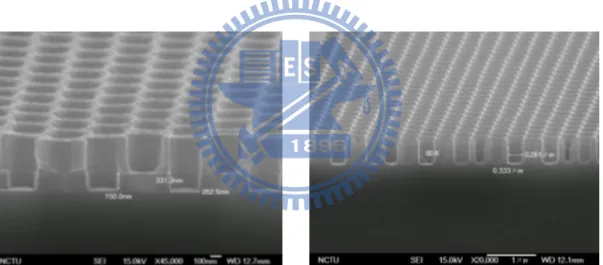
structure of (a) D=600nm ; H=200nm (b) D=600nm ; H=400nm (c) D=1000nm ; H=200nm (d) D=1000nm ; H=800nm…………...49 Figure 5.3-3 The TEM image of the patterned glass substrate a-Si thin film
solar cell (D=1000nm; H=200nm)……….……..50 Figure 5.3-4 The TEM image of the patterned glass substrate a-Si thin film
solar cell (D=1000nm; H=200nm) with higher magnification…….50 Figure 5.4-1 The calculated short-circuit current density Jsc (mA/cm2) as
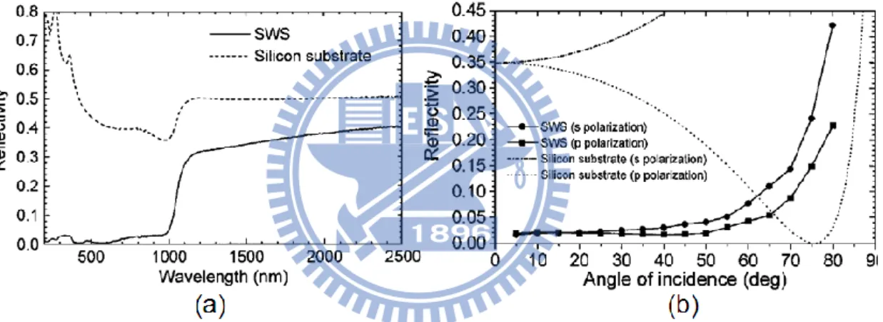
a function of the diameter D and height H………...…52 Figure 5.5-1 The measured reflectance of the biomimetic glass substrate, flat
glass substrate, Asahi-U glass substrate a-Si solar cell at normal incident condition……….53 Figure 5.7-1 The measured current-voltage characteristics of flat glass cell,
Asahi-U glass cell, biomimetic glass cell (D=600nm H=200nm; D=600nm H=400nm; D=1um H=200nm; D=1um; H=800nm).…..56 Figure 5.8-1 The measured external quantum efficiency of flat glass cell,
Asahi-U glass cell, biomimetic glass cell with the smallest H/D ratio sample (D=1000nm; H=200nm)………..59 Figure5.9-1 The influence of H/D ratio to VOC, JSC,
1
Chapter 1. Introduction
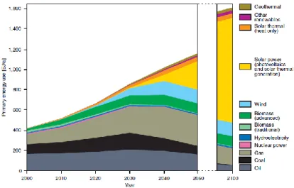
Due to the fuels shortage and greenhouse effect, the energy issues have become a serious problem in the future. According to the BP2009 World Nuclear Association, about 1.258 trillion barrels of oil reserves which is about 42 years usage amount, and 185 trillion cubic meters fuel gas reserves which is about 60 years usage amount, about 826 billion metric tons coal reserves which is about 122 years usage amount, 547 metric tons uranium ore reserves which is about 124.6 years usage amount. In the renewable energy, which including solar energy, hydropower, wind power, fuel cells, only solar cells is a one-step conversion process which directly convert sunlight into electricity. Solar energy is also a very environmental protection renewable energy, the process converting sunlight to electricity does not produce waste and exhaust emissions, so it will not produce any pollution to water, air, and soil. However, as industrial development and the rising of the living standards the demand for energy is increased. The excessive use of natural resources result in global warming effect and making the global temperatures rising, and the global natural environment is deteriorating rapidly. The radiation power of sun to earth per year is about 600 megawatts, if we can use the solar energy effectively, we can not only solve the threat of energy depletion, but also solve the environmental problems caused by the greenhouse effect. Therefore solar energy will be the most important renewable energy source in the future. (Figure 1-1).
2
Figure 1-1 The amount of energy usage in next 100 years (German Advisory Council on Global Change WBGU Berlin 2003)
1.2 Brief development of the solar cell
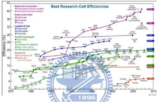
Generally there are two major types of solar cell, the first one is organic solar cell and the second one is inorganic solar cell. Due to the short lifetime and low conversion efficiency, the development of organic solar cell was limited. There are many types of inorganic solar cells, the main solar cells materials are compound semiconductor materials which include Ⅱ - Ⅵ and Ⅲ - Ⅴ, silicon (crystalline, poly-crystalline, amorphous)[1-3]. Figure 1.2-1 shows the highest conversion efficiency of various solar cells. The lowest-cost thin film solar cell is Ⅱ - Ⅵ compound materials (CdTe / CdS), the module production power conversion efficiency is about 10.5% [4], and the life time is about 25 years, however, due to cadmium inhalation or ingestion will accumulate in the human liver and cause kidney poisoning, therefore the manufacturing processes waste which will cause environmental issues. The advantage of Ⅲ - Ⅴ compound solar cells is ultrahigh power conversion efficiency, the power conversion efficiency of single-junction GaAs
3
solar cell is about 18% [5] and the efficiency of the three junction of Ⅲ - Ⅴ solar cells can up to 30% [6], furthermore it has a good anti-radiation property so it is very suitable for the satellites or space application. However, the cost of Ⅲ - Ⅴ compound wafer is very high, such as GaAs , InP, etc., and it is a complex epitaxial technology, so it is not suitable for universal power applied to the people's livelihood. The way to reduce the cost of Ⅲ - Ⅴ solar cells is using concentrating system, which can greatly reduce the usage of Ⅲ - Ⅴ material furthermore to reduce the costs.
Silicon base material which include single crystalline silicon, polycrystalline silicon and amorphous silicon, because of the mature process technology of single crystalline silicon and poly crystalline silicon materials, so the earliest solar cell was the crystalline silicon solar cells and the power conversion efficiency of single crystalline silicon solar cell is around 20%, so the market share of crystalline silicon solar cells is nearly 90%.
However, compare to oil power($ 3.5 / W) the cost of solar power is still too expensive. If the cost of solar energy is down to $ 0.5 / W which is the same as the cost of oil power, then the world's energy use patterns will be in revolutionary changes. The high cost of crystalline silicon solar cells are due to the high energy demand when it was fabricated and high-purity silicon requirement. The silicon thin film solar cells reduce energy demand and consumption of materials significantly. The advantages of thin film solar cells which includes low demand for materials, low cost, low weight, large area manufacturing, even the flexible characteristics etc., so thin-film solar cells is currently a major goal for the international solar cell manufacturers and R & D team. Figure 1.3 shows 2009~2010 global solar cell market share statistics, which account is about 85 % for crystalline silicon solar cells and 15% market share for thin-film solar cells, and the total solar power generation
4
from 2009 to 2010 is from 7.9GW to 15.4GW [7]. Considering to the content of material, silicon is the second abundant element on earth, and the silicon metrial process technology is very mature, so the silicon thin-film solar cell is still the focus of development of industrial production, so estimates 2050 global solar cell market share the market share of silicon base solar cell can maintain about 80%.
Figure 1.2-1 The highest conversion efficiency of various solar cells (Res. Appl.17, 85-94 2009)
5
1.3 The advantages and the challenge of thin-film solar cells
The key points of solar energy are the power conversion efficiency and the costs. Currently, the single crystalline silicon wafers and polycrystalline silicon wafer are still the main materials of solar cell, but limited to the high energy consumption and the high-purity materials requirement which is hard to reduce the cost of single crystalline solar cell and polycrystalline silicon solar cell.
Thin-film technology is a good way to reduce the consumption of fabrication energy and reduce the consumption of material. There are three major material of production thin film solar cell which includes CdTe, CIGS and silicon. Considering to the content of material, silicon is the second abundant element on earth, and the silicon metrial process technology is very mature, so the a-Si thin-film solar cell is still the focus of development of industrial production. As we mention before, it is not easy to reduce the cost of the first generation solar cells, so the second-generation thin film solar cells is need to develop. The advantages of thin film solar cells which includes low demand for materials, low cost, low weight, large area manufacturing, even the flexible characteristics etc.
Especially for a-Si thin film solar cell due to the thin active layer (<1um) and the minority carrier diffusion length is typically limited to 300 nm [8,9], which result in a mismatch of light absorption depth and minority diffusion so it shows a low light absorption at near-infrared. As the result, we have to solve this problem further to enhance the conversion efficiency of a-Si thin film solar cell.
6 1.4 Motivation
The features of the future solar cell are as following, thin film, low-cost, high efficiency, so the amorphous silicon (a-Si) thin film solar cell was considered for future generation of photovoltaics applications, due to the low cost. But due to the thin active layer (<1um), it shows a low absorption coefficient at near-infrared region. How to improve light harvesting is a very important issue in high efficiency a-Si thin film solar cell. And due to the different refractive indices of the material interface, there exists a Fresnel reflection which will cause certain loss in incident light.
So antireflection and light trapping are key techniques for efficiently harvesting solar photon. Several studies of sub-micrometer gratings (SMG) structure demonstrate the SMG structure offer a graded refraction index interface, and shown ultra-low reflectivity, another feature of SMG structure is diffraction of light, to get longer optical path length, further to enhance the light absorption in a-Si thin film.
In this study we want to fabricate a glass substrate with SMG structure and applied on a-Si thin film solar cell. We expect the cell will possess the nice antireflection and light trapping characteristics, further to enhance the conversion efficiency of a-Si thin film solar cell.
7
Chapter 2. The physics of solar cells and brief introduction of
amorphous silicon
2.1 The fundamental structure of solar cell
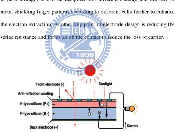
A complete solar cell structure design was shown in Figure 2.1-1 [10.11], there is a glass protective layer (cover glass) and a transparent adhesive layer outside, which play the role of fixed and the protection of the internal components of solar cells are not damage by the environment water vapor and other material. According to their function the internal components of solar cell, they can be divided into three parts, the first one is the anti-reflective layer (antireflection coating), which improve the light harvesting in solar cell by the optical design further to reduce optical losses due to the reflection; The second one is the semiconductor pn junction (active layer), the pn junction can absorb the light and generate the electron-hole pair and then separate the electron and hole which diffuse to the electric field the between the pn junction. The third one is electrode, which extract the carrier. The front electrode which allows light to pass through so it will be designed into different spacing and the rate of metal shielding finger patterns according to different cells, back electrode which with the whole plane structure, and reflect the light which one is incomplete absorbed at once optical path back to the active layer and increase the power conversion efficiency. By using the load of outside circuit, the photocurrent can change into to an output power. For enhancing the power efficiency of solar cell, there are three keys can be improved.
(i) Enhancing the photon collection, the implementation is an anti-reflective layer, an effective anti-reflective layer in solar cells which should have features of broadband and omnidirectional anti-reflective characteristics, and increase the photo collection per unit area of solar cells.
8
(ii) Enhancing the internal quantum efficiency (IQE), the implementation is improving the quality of semiconductor material. Reducing the semiconductor material defect at manufacturing process or reducing opportunity of the carrier recombines by defect. Developing high-quality solar material or by epitaxial process to create the most suitable structure for photovoltaic which improve the solar energy conversion efficiency and has a broadband absorption spectrum.
(iii) Enhancing the electron extraction (Carrier collection), the implementation is to develop a high-quality electrodes. The front electrode which allows light to pass through, it will be designed into different spacing and the rate of metal shielding finger patterns according to different cells further to enhance the electron extraction. Another key point of electrode design is reducing the series resistance and forms an ohmic contact to reduce the loss of carrier.
9 2.2 The physics of solar cells
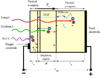
Typically, solar cell was formed as a diode, and there is a pn junction between the n-type and p-type semiconductor, due to the different concentration of electron and hole, carrier diffusion will occur and result in diffusion current. In the vicinity of the junction, the electron concentration of n-type is higher than the electron concentration in p-type, so the electron will diffuse form n-type to p-type. Similarly, the hole concentration of p-type is higher than the hole concentration in n-type, so the hole will diffuse form p-type to n-type, so the neutral will be broken. The junction at the n-type side will exist the positive charges which were caused by the donor, and the junction at the p-type side will exist the negative charges which were caused by the acceptor. The region with n-type positive charges and p-type negative charges which we called space charge region, and there is an electrical field in the space charge region and the direction is from n-type side to p-type side.
When the light with the energy higher than the band gap of the semiconductor was incident, the light will be absorbed then transfer the energy to electrons, and then the electron are excited to a higher energy state which resulting in an electron - hole pairs. Due to the built-in electrical fields the electrons will move to the n-type region and the holes will move to the p-type region. The electron hole pairs move by the built-in electrical fields will result in drift current.
The basic working principle of solar cells is separate the electron hole pairs by using the built-in electrical field in the space charge region before they recombine. Figure 2.2-1 shows the diffusion mechanism and drift mechanism when the light incident into the solar cell, the photocurrent is the sum of diffusion current and drift current [12.13]. If we make a contact with two terminals in a diode, it is called short circuit and the current was called short circuit current which equal to photocurrent. If there is no contact with two terminals in a diode, it is called open circuit, when the
10
light incident, the electron will accumulate at n-type side and the hole will accumulate at p-type side which results in a photo-voltage or called open circuit voltage.
Figure 2.2-1 Illustrations of the carrier generation, carrier diffusion and carrier drift in solar cell
Figure 2.2-2 shows the solar cell’s equivalent circuit, which contains an ideal pn junction diode, current source ( Iph), series resistance (Rs) and shunt resistance
(Rsh).
11
According to the Cauchy Hoff's law, the output current density (J) can be presented as formula 2.2-1. sh s nkT JAR V q sc R JAR V e J J J s ( 1) ) ( 0 (2.2-1)
Jsc is photocurrent which is the current generated by illumination and deducts
the surface recombination at the two terminals of diode. J0 is the reverse saturation
current density, it will increase when the forward bias increased. T is temperature, n is the ideal factor. For easier analysis, we consider the solar cell is in ideal conditions (Rs=0, Rsh→∞, n=1), so the formula2.2-1 can be written into formula 2.2-2.
0(
1
)
nkT qV scJ
e
J
J
(2.2-2)2.3 The parameter of solar cells
a. Short-circuit current density (JSC)
The short circuit current is a current when the solar cells were under illumination, and with a zero external load, it means the solar cell circuit is short circuit. From formula 2.2-2, for the ideally solar cell, which the series resistor is nearly to zero, and the shunt resistor is nearly to infinity, so the formula 2.2-2 can be written into formula 2.3-1.
nkT sc qV sc I e I I V I( ) ( B 1) 0 (2.3-1)
b. Open circuit current (VOC)
The open circuit voltage is a voltage when the solar cells were under illumination, and with an infinite external load, it means the solar cell circuit is open
12
circuit, at this time the output current is zero, for the ideally solar cell, the ideally factor is 1(n=1), the formula 2.3-1 can be written into formula 2.3-2.
] 1 ln[ 0 I I q kT V SC oc (2.3-2)
From formula 2.3-2 the VOC increase with the ISC and I0 decrease. The I0 were
related to the band gap and doping concentration of semiconductor device so the open circuit voltage is also related to semiconductor’s band gap and doping concentration.
c. fill factor (FF)
When the solar cell is operating at the maximum output power which has the voltage VM with a corresponding current IM. The fill factor is defined as formula 2.3.2,
which means the ratio of the product square (VM×IM and ISC×VOC) of I-V curve, so the
the series resistance and shunt resistance will affect the fill factor.
100% 100% sc oc MP MP sc oc MP I V I V I V P FF (2.3-2) d. Conversion efficiency (η)
The conversion efficiency of solar cell is defined as the ratio of maximum output
power (PM) and incident light power (Pin). Conversion efficiency can be express as
fomular 2.3-3. in sc oc in m m in m P FF I V P I V P P
(2.3-3)13 e. quantum efficiency (QE)
Quantum efficiency is an important parameter for solar cells, which means the ratio of incident photon conversion into electron-hole pairs. There are two types of quantum efficiency, the first one is external quantum efficiency (EQE) and another one is internal quantum efficiency (IQE). The external quantum efficiency is the ratio of incident photons conversion to electrons and delivered to the external circuit. The internal quantum efficiency is the ratio of incident photons conversion to electrons inside the device. The IQE is simply response the effects of recombination losses inside the semiconductor material which only related to the quality and absorption coefficient of the material. The external quantum efficiency is not only includes the effect of internal quantum efficiency but also the carrier collection ratio of electrode and other losses outside the device. The relation between the external quantum efficiency and internal quantum efficiency is as formula 2.3-4. The relation between the external quantum efficiency and short-circuit current density is as formula 2.3-5 which the bs(E) is the photon flux (s-1m-2eV-1).
)
(
)
(
1
)
(
)
(
T
R
EQE
IQE
(2.3-4)J
SC
q
b
S(
E
)
QE
(
E
)
dE
(2.3-5)2.4 Brief introduction of amorphous silicon
2.4.1 Brief history of amorphous silicon
Silicon base thin-film solar cell is start from amorphous silicon. Amorphous silicon thin film has an unique physical characteristics, and it can process in large area, so amorphous silicon have been widely used in industry. In 1965 Sterling and Swann
14
who are the first two scientists use the radio frequency glow discharge to decomposition the silane (SiH4), further to manufacture the amorphous silicon thin
film [14]. In 1969 Chittick who point out the amorphous silicon thin film made by glow discharge method which has the better optical conductivity than the amorphous silicon thin film made by sputtering method [15], at the same time they also point out the possibility of doping in amorphous silicon. In 1972 Spear and LeComber manufacture n-type and p-type amorphous silicon thin film by inducing the PH3 and
B2H6 gas, while the same year, Triska confirmed that the amorphous silicon thin film
made by pure silane which also contains hydrogen atoms and shows a good electrical properties which is actually contributed by the structure of hydrogen atoms bond with silicon atoms and this amorphous silicon was called hydrogenated amorphous silicon (a-Si: H).
2.4.2 The characteristics of amorphous silicon thin film
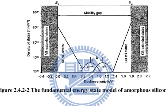
From Fig 2.4.2-1 the structure of amorphous silicon (a-Si) which is a structure with periodic atoms arrangement in a small area but a random atoms arrangement in large area, and there is a poor bonding energy between silicon atoms so it is easily to broken and forming dangling bond, these dangling bond cause a large defect density in amorphous silicon. Generally, the defect density of amorphous silicon is about 1021cm-3, in order to reduce the dangling bond density, hydrogen will be induced during the manufacturing process to passivation (a-Si: H), hydrogen atoms can bond with dangling bond further to reduce the density of dangling bond.
Because of the atoms arrangement of amorphous silicon is a random arrangement, so the band gap definition of amorphous structure is not as the same as crystalline structure, because of in amorphous semiconductor there are some band tail at the edge of conduction band and valence band and these band tail which is caused
15
by random atoms arrangement. In addition, defects can also form a defect state which located in the middle of the band gap, and these defects generate a continue state between conduction band and valence band, which is totally different with the band gap of crystalline silicon, any state between conduction band and valence band are not allow, so we cannot define the band gap of amorphous silicon clearly.
We will re-define the band gap and the energy state of amorphous silicon. Firstly, instead of the strict definition of the highest energy of valence band and the lowest energy of conduction band of crystalline silicon, there is a similar definition which is called mobility edges as indicated by the symbol EC and EV. The energy state
is divided into two parts: first one is extended states which is the energy state with the energy at E <EV and E> EC; the second one is localized states (localized states) which
is the energy state with the energy at EC> E> EV. The carrier mobility in amorphous
silicon is very low, in usually the electron mobility is around 1 ~ 10cm2 / (V.s) and the hole mobility is around 0.01 ~ 0.1cm2 / (V.s). The carrier mobility is near zero when the carrier is in localized states, usually the carrier mobility was cause by the mechanism of thermal effect or tunneling effect which we called hopping, therefore, the difference between the EC and EV at mobility edge was called the mobility gap,
and this band gap does not have meaning of forbidden gap. The general mobility gap of amorphous silicon is around 1.7 ~ 1.8eV. Figure 2.4.2-2 is the fundamental model of amorphous silicon energy state, we can describe the band tail and defect state by using mathematics model. As near the central of mobility edge the mobility edge defect density of valence band and conduction band is exponential decay. The defect states are located in the middle of mobility gap and with a Gaussian distribution.
16
Fig 2.4.2-1 The 1.atomic arrangement of crystalline, poly, amorphous silicon
Figure 2.4.2-2 The fundamental energy state model of amorphous silicon
Hydrogenated amorphous silicon thin-film is the alloy of silicon atoms and hydrogen atoms, the ratio of silicon and hydrogen and bonding structure will affect the film material, optical and electrical properties. Typically, there is a Staebler-Wronski effect in amorphous silicon application [16], this effect will lead to light-induced degradation [14.15]. Due to the great defect amount of amorphous silicon, after 1000 hours illumination the performance of amorphous silicon will shows a sharp decline, it is caused by the bonding structural changes due to illumination.
The most basic features of amorphous silicon is the special arrangement of atoms which shows an order arrangement in short-range and disorder arrangement in
17
long-range which is a random network of covalent atomic structure, it is means for a single silicon atom the covalent bonds is form by four silicon atoms just as the same as single crystalline silicon and it is regularly arrangement for neighboring atoms, but there is an irregular arrangement for distant atoms.
Amorphous silicon is the direct band gap material, so the light absorption coefficient of amorphous silicon is very large and the energy gap is around 1.7eV. However, the energy gap of amorphous silicon is tunable by different alloy ratio, and the tunable range is about 1.4eV ~ 2.0eV.
18
Chapter3. Experimental Instruments and Methods
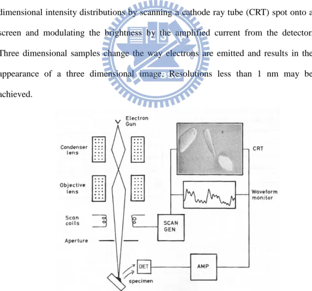
3.1 Scanning Electron Microsope (SEM)The electron microscope uses electromagnetic lenses to focus the beam to produce an image. However, SEM and TEM differ in the way images are produced and magnified. SEM is used to view the surface or near surface of a sample, whereas TEM provides information of the internal structure of thin specimens. The scanning electron microscope as the name suggests scans across the specimen by the scan coils.
As the sample is scanned by the electron beam as shown in figure 3.1-1, it emits electrons and electromagnetic radiation. A detector counts the low energy secondary electrons (< 50 eV) or other radiation emitted. The image is produced by two dimensional intensity distributions by scanning a cathode ray tube (CRT) spot onto a screen and modulating the brightness by the amplified current from the detector. Three dimensional samples change the way electrons are emitted and results in the appearance of a three dimensional image. Resolutions less than 1 nm may be achieved.
19 3.2 Transmission electron microscope (TEM)
TEM is a method of imaging where a beam of electrons are directed through a sample after which they are scattered into discrete diffracted beams. The diffracted electron beams are then focused in the back focal plane of the objective lens. TEM may have two modes. When operated in diffraction mode, the diffraction lens is focused on the back focal plane to produce a diffraction pattern. For the imaging mode, the diffraction lens is focused on the first image plane to produce a magnified image. In addition, the beam may be allowed to pass through the sample to obtain a bright-field image however the diffracted beams produce a dark-field image.
The ray diagram (Figure 3.2-1) shows (a) imaging projecting a diffraction pattern and (b) projection of an image onto a viewing screen. The interaction of the electron beam with crystalline material tends to be by diffraction. The orientation of the planes of atoms in the crystal to the electron beam changes the intensity of diffraction. TEM equipment often uses a goniometer to allow the sample to be tilted to a range of angles to obtain specific diffraction conditions. Diffracted electrons are also selected using different apertures. The intensity of diffraction is a maximum at the Bragg angle, although a variation of diffraction intensity occurs with deviation from the Bragg angle. This also depends on the thickness of the specimen. The thinner the crystal sample, the further the crystal may deviate from the Bragg condition.
20
Figure 3.2-1 Ray diagram showing two basic operations of TEM.
3.3 Angle resolved Integrating sphere reflectance measurements
Figure 3-3-1 shows a traditional reflectivity measurements setup which includes a single wavelength light source and a photon detector. According to the law of reflection we can set a detector at the corresponding position with the incident light and we can measure the reflectance of the surface, but this is just suit for non-rough surface. In our experiment, we want to measure the reflectance of biomimetic surface (rough surface), when the light incident into the rough surface it will be scattering, the reflective light will appear in each direction, so we cannot just set a detector at specific position.
21
Figure 3.3-1 The schematic of traditional reflectivity measurements system.
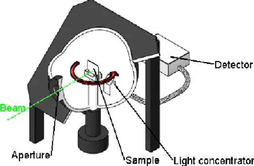
Figure 3.3-2 shows the setup of our angle resolved integrating sphere reflectance measurements system. In this system, we use a fiber to induce light into a convex to confirm the incident light is a parallel light source and then incident into the aperture of the integrating spheres. Because the solar spectrum include all wavelength from UV to infrared, we need to understand the reflectance of each wavelength, so we change the single wavelength light source into a xenon light source which is a wide wavelength light source. In order to measure the reflectance of rough surface, our approach is use an integrating sphere to collect all the reflective light in each direction, the reflective light will be trap in the integrating sphere and finally it will be detected. In addition, this system has a rotating carrier stage, that we can measure the angle-dependent reflection properties of the rough surface.
22
Figure 3.3-2 The schematic of the angle resolved integrating sphere reflectance measurements system
3.4 Current-voltage measurement (J-V curve)
Figure 3.4-1 shows the setup of the solar cell Current-voltage measurement. In this study, the solar cell power conversion efficiency measurement system which includes, 1000W ClassA AM1.5 G solar spectrum which made by Newport company and calibrated with Renewable Energy Laboratory (NREL) and there is only 2% of error at each wavelength in international standards solar spectrum, then corrected incident sun light power intensity of 1 sun and maintain the temperature for the 25 ° C through the temperature control system. The current - voltage characteristics was measured by Keithley 2400 source meter and control by labview program.
23
Figure 3.4-1 The schematic of Current-voltage measurement system
Solar cell current - voltage (I-V) characteristics was measured under the simulated sunlight AM1.5G illumination conditions, the conducting measured. By the current - voltage measurements, we can get some important parameters to analysis the characteristics of solar cells which include short circuit current (JSC), open circuit
voltage (VOC), fill factor (FF), conversion efficiency (η), the maximum power output
voltage (VMP), the maximum power output current (IMP), series resistance (Rs), and
shunt resistance (Rsh).
3.5 External quantum efficiency measurement
Measuring the external quantum efficiency (QE (λ)), also known as spectral response (SR (λ)) is very important for understanding the carrier generation and the diffusion mechanism of photovoltaic device. The unit of spectral is the amperage of current generate from per wattage of incident light (A / W). Formula3.5-1 shows the mathematical formula of external quantum efficiency, which indicate the probability of incident photon transform to electron-hole pairs.
hc qSR QE
) ( ) ( (3.5-1)24
We assume that the operating point of maximum power output and short-circuit are the same, so usually the spectral response is the short circuit current. During solar cell research there are several systems of external quantum efficiency measurement, such as interference filter, grating spectrometer etc... For single-junction solar cells we use the periodic single-frequency light to irradiate solar cell and measure the photocurrent then usinglock-in amplifier to transfer the signal into AC signal. In our experiment we usea grating spectrometer system for broadband spectral measurements (400-3200 nm) and for high spectral resolution, the setup is as figure 3.5-1 [13]. Xenon lamp with wide spectrum when the wide spectrum light pass through a grating it will become a single frequency light and then focus on the solar cell. The aberration can be solved by using a spherical mirror or a parabolic mirror.
25
Chapter4. The review of nanostructure fabrication
For high efficiency solar cells we have to reduce the surface reflectance when the light incident into the device. Due to the different refractive index of the material interface, there exists a Fresnel reflection. Fresnel reflection of incident light arises from the large refractive index discontinuity at the interface of two medium. For example, the high reflective index of Si results in optical reflection loss up to 37% for the incident light, which severely limits the performance of optoelectronic devices [18], therefore, effective antireflective coatings (ARCs) are particularly important.
Traditionally, we use plasma-enhanced chemical vapor deposition (PECVD) to depose the dielectric films, such as silicon nitride (SiNx), silicon dioxide (SiO2) and
other materials to be anti-reflective coating (ARC), based on different refractive index to determine the thickness of anti-reflective coating which the thickness is the odd multiple of quarter incident light wavelength [19-22] to generate the destructive interference further to reduce the reflectance. But the single layer ARC can reduce the reflectance for a specific wavelength only. For example we usually use the 80nm thickness of SiNx to reduce the wavelength of 600nm which is a wavelength who just mapping to the highest power of solar spectrum, but at another wavelength the reflectance is still high. Therefore, finding more efficient and broadband anti-reflection coating has become an important issue.
Figure 4-1 The working principle of quarter wavelength thickness AR coating[23]
26
In 1983, W.H. Southwell [21] proposed a theory of graded refractive index
anti-reflection coating which possess a broadband and omnidirectional
anti-reflective characteristic. The theory mentions that if the refractive index between two dielectrics is a gradual change, it will enable decline the reflectance dramatically, we can use multi-layer materials to approach this effect. Then in 2002, J.A. Dobrowolski optimized refractive index distribution by simulation [19,20]. The reflectance at near-infrared range is still less than 1%, and when the light at 85-degree angle of incidence, the reflectance is still very low.
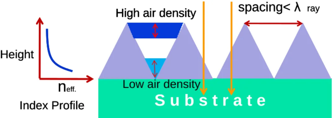
In recent years, the nanotechnology is rapid progress, we can use a graded
structural to approach the effect of graded refractive index, the scale of such structures are less than a wavelength which we called sub-wavelength structures (SWS) [24, 25]. The SWS is shown in Figure 4-2. Because the spatial proportion of refractive index is gradual change, it will reduce the different of refractive index further to reduce the reflectance. We can get the broadband and omnidirectional anti-reflective characteristic by using the SWS. Simply, we can just image that is an infinite superposition of multi-layer gradual change refractive index film, the refractive index difference between two layers is very small, so from formula 4-1, the transmittance is nearly 1 which means the reflectance is nearly zero.
) ( , 1 ) ( 4 2 1 2 2 1 2 1 n n n n n n T (4-1)
27
Figure 4-2 Illustrations of the SWS AR coating and the concept of graded index
interface
Figure4-3 shows the moth eye which has a corneal nipples array on the surface; because of the spatial proportion of nanostructure it will approach the graded refraction index interface, and enhancing the transmittance. In recent years, using the biomimetic structure for solar cell anti-reflective layer has become a major trend, hoping to use the spatial proportion of nanostructure to approach the graded refractive index further to reduce the reflectance. We will introduce some important nanotechnology at the following section, which include photolithography, electron beam lithography, nano-imprinting, nanosphere lithography.
Figure4-3 The picture of the moth’s eye
S u b s t r a t e
spacing<
λ
ray High air densityLow air density
n
eff. HeightIndex Profile
S u b s t r a t e
S u b s t r a t e
spacing<
λ
ray High air densityHigh air density
Low air density
n
eff. Height28 4.1. Photolithography [wiki]
Photolithography is a process used in micro scale or nano scale fabrication to selectively remove parts of a thin film or the bulk of a substrate. It uses exposure unit to transfer a pattern from a photo mask to a photoresist, and the sample was etched by using the photoresist etching mask, and then transfer a pattern from a photoresist to a thin film or a bulk.
The disadvantage of photolithography include hard to large area of production, high cost of photo mask production, process complexity, and due to the diffraction effect it is not easy to make the nano-scale structure. Figure 4.1-1 shows the periodic nanostructures produced by photolithography.
Figure 4.1-1 The SEM image of nanostructure made by photolithography technology (a) SiNx (b) GaAs (NCTU NFC)
4.2 E-beam lithography
With the requirements miniaturization of electronic device, due to the diffraction effect the traditional photolithography processes is not easy to make the nano-scale structure. Therefore there many exposure light source was developed to replace the traditional photolithography exposure light source to solve this problem, such as Xray, extreme UV, electron beam lithography and ion beam lithography.
29
However, electron beam lithography has high-resolution characteristic and high accuracy of focus, so it becomes a nice choice for nano-scale process.
The principle of electron beam lithography is use the accelerated electrons through the high voltage coil, directly pattern the graph on the sensitizer and then to exposure, the process is somewhat similar to the photolithography process, the different between photolithography and electron beam lithography which is just use the different photoresistor , and the exposure light source change from photon into electron. Electron-beam lithography system can accurately produce nanostructures, but the disadvantage is high cost, very low throughput, so the electron-beam lithography is not suit for solar cell application which is always applied in large area.
In 1999, Y. Kanamori [26], who use electron-beam lithography technology to produce two dimensional sub-wavelength structures, this experiment product a 1.44 mm2 silicon substrate with two dimensional sub-wavelength structures and it takes 10.8 hours to fabricate, the process and side view are shown in Figure 4.2-1(a)(b) and the reflectance is shown in Figure 4.2-2. The reflectance of this sample is less than 3% at the wavelength range between 200nm to 1000nm. But electron-beam lithography apply in solar cell is limited by the high cost and low throughput of this technology.
30
Figure 4.2-1 (a) The SEM image of nanostructure made by E-beam lithography (b) The illustrations of E-beam lithography process.
Figure 4.2-2 The reflectance of the nanostructure made by E-beam lithography.
4.3 Nanoimprint lithography
Compared to electron beam lithography, nanoimprint lithography has the advantage of low cost and high throughput. Nanoimprint technology apply in the the compact disk (CD) has been developed for a long time, due to the technological breakthroughs, nanoimprint lithography can create a nano structure as small as 10nm, due to the low cost and high throughput, nanoimprint is very suitable for solar cell application, but it is hard to make a master mold and a master mold can be reused about 50 times.
31
The manufacturing methods of master mold are generally photolithography processes and laser micro-machining. The cost of laser processing is lower than photolithography, but accuracy is poor (depending on the size of the laser beam). Figure 4.3-1 shows the nanoimprinting technology manufacturing processes, the first step is the graphics processing, and you can choose to use photolithography techniques or laser exposure processing to define the graph. The second step is making the initial layer by thermal evaporation. The third step is plating metal by using plating technology. The fourth step is to polish metal surface, if we do not polish the surface, it will cause an uneven pressure when we are imprinting. The fifth step is to remove the polymer by using chemical solvent, at this time we can get the metal master mold. The sixth step is transfer the graph of metal master mold to polymer materials. The seventh step to remove the metal master mold and get the master mold. Figure 4.3-2 (a) shows a SEM image of master mold. Figure 4.3-2 (b) shows the nanostructure made by nanoimprinting.
In 1995, SY Chou who uses the nanoimprinting technology to made 25nm line width of the structure [27]. Unlike conventional lithography process, nanoimprinting process didn’t need any energy beam or electron beam, so there is no diffraction, scattering effect during the process. In recent years, the scale of nanostructure made by nanoimprinting process can be reach as small as 5nm [27], and the aspect ratio can be reach as 20 [28].
32
Figure 4.3-1 Illustrations of the nanoimprinting technology manufacturing processes.[29]
Figure 4.3-2 (a) The SEM image of the master mold of nanoimprinting technology (b) The SEM image of the nanostructure made by nanoimprinting
technology.[29]
Therefore, using nanoimprint technology in anti-reflective nanostructure layer has become an important research topic. In reference [30], the measure results is as same RCWA simulation results (Figure 4.3-3), the transmittance of graded refractive index is higher than the PMMA film.
33
Figure 4.3-3 (a) The RCWA transmittance simulation result of pyramid structure (b) The comparison of the measure reflectance and the simulation reflectance of
pyramid structure.
4.4 Nanosphere Lithography (NSL)
The other name of this method is called colloidal lithography. This method is generally included two parts, the first one is close package arrangement and single layer nanoparticles, which treated as an etching sacrificial mask, the second one is anisotropic reactive ion etching, due to the different etching selectivity of the nanosphere and semiconductor material, and then form the nanostructure. Compared with electron beam lithography, nano-imprinting lithography, etc…, nanosphere lithography doesn’t need to use the sophisticated and expensive equipment, so it is fast and low cost. How to form a single layer and hexagonal arrangement of nanoparticles, and reduce the arrangement defects which becomes the important keys of nanosphere lithography.
There are several methods to create a large area and periodic nanoshpere arrangement which include self-assemble via liquid-air interface method, spin coating method, Langmuir-Blodgett method.
34 Self-assemble via liquid-air interface
In reference [31], it uses the self-assemble via liquid-air interface method to form a single layer and hexagonal arrangement of polystyrene nanospheres. These treated polyethylene nanospheres has a carboxyl group on the surface so it is provide with a hydrophilic end. Because of the different sizes of nanosphere so the carboxyl group ratio on the sphere surface will be different. This study indicates that the ratio of carboxyl group on the sphere surface will affect the arrangement of polystyrene nanospheres.
The polystyrene nanoparticles suspension with a ratio of 1:1 mixed with alcohol and then dripping into the pure water. We can use some compression roll bar and slow drainage to control the position of the single layer nanospheres and then put on the substrates. We can observe the uniformity of the substrate surface to confirm the uniformity of self-assemble nanospheres. Another research [32] is use ODT to support the arrangement of nanospheres in liquid-gas interface to form a single layer of nanospheres.
Figure 4.4-1 (a) Illustration of Self-assemble via liquid-air interface method system (b) The process of Self-assemble via liquid-air interface method
35 Spin coating method
The reproducibility of spin-coating method is very difficult. Peng Jiang [33] uses the ETPTA as a solvent to approach the single layer arrangement of silica nanosphere, but it is not a close package arrangement, he using the different spin speed to control the stack layers of silica nanosphere, after spin coating process the oxygen plasma was used to remove the ETPTA.
Figure 4.4-2 (a) Illustration of the ETPTA remove by O2 plasma. (b) The picture
of the silica on 4 inchs wafer by using spin coating method and the Fourier transform result of the silica arrangement.
Langmuir-Blodgett method (LB method)
Langmuir-Blodgett method or called dip coating method, this method uses the
speed and direction of stepper motor, the solution evaporation speed, or chemical solution nature to control the arrangement of nanospheres. The maximum size of nanosphere arrangement by using LB method is around 4 inchs [34.35], and the advantage of this method is the excess nanosphere can be reused which can reduce the
36 cost of LB method.
Figure 4.4-3 (a) Illustration of the Langmuir-Blodgett method system setup. [36]
Figure 4.4-4 The picture of the close package nanosphere arrangement in wafer scale area.