3 – 10 GHz ultra-wideband low-noise
amplifier with new matching technique
C.-P. Liang, C.-W. Huang, Y.-K. Lin and S.-J. Chung
A low-power and low-noise amplifier with a new input- matching tech-nique using 0.18 mm CMOS technology for ultra-wideband appli-cations is presented. A proposed broadband input match can be acquired easily by selecting an appropriate width of the transistor, which will effectively avoid the usage of the low-Q on-chip inductors in the input network. Moreover, demonstrated is the feasibility of the inter-stage resonator to accomplish bandwidth enhancement without additional power consumption. The IC prototype achieves good per-formances such as a power gain of 16.2 dB, a better than 10 dB input return loss, and 2.3 dB minimum noise figure while consuming a DC core power of only 6.8 mW.
Introduction: Ultra-wideband (UWB) systems operate over a wide range of frequencies from 3.1 to 10.6 GHz, and the realisation of the UWB receiver suffers serious challenges, especially for the low-noise amplifier (LNA). It must provide a fine wideband 50 V input matching with flat gain over the entire bandwidth, low noise, good linearity, and low power consumption. In general, the distributed configuration[1]
and LC input network[2, 3]are attractive for their ultra-wide bandwidth; however, major drawbacks are the larger chip area and worse noise figure owing to use of low-Q on-chip inductors in the input network. To overcome the above-mentioned drawbacks, in this Letter we propose a new inductorless input-matching technique, which is based on a source-degenerated structure to achieve superior noise performance. On the other hand, the common-source stage with LC tank load can be adopted to enhance the bandwidth of the amplifier by appropriately tuning the resonator frequency of the LC tank load; however, it is una-voidable to increase DC power consumption, which may make this circuit unsatisfactory for low-power application. In this Letter, we utilise the inter-stage resonator to improve power gain bandwidth without using the common-source stage. As a consequence, DC power reduction and bandwidth enhancement will be attained simultaneously.
Ca with w0 wH Vdd1 Ls Ls Vin Ca M1p M1n a b c Vdd1 Ls CB Cgs2 Ls Rg Rg Vin M1n M1p M2 Vg1 Vg2
Fig. 1 Principle of proposed input matching circuit a Current-reused configuration with additional capacitor Ca
b Frequency behaviour of input impedance with and without capacitor Ca
c Proposed broadband input match circuit with suitable size of transistor M2
Circuit design: The proposed input matching circuit, as shown in
Fig. 1a, utilises the current-reused configuration with an additional
capacitor Cato achieve the design of low-power characteristic and
wide-band match.Fig. 1bdepicts the frequency behaviour of the input impe-dance on the Smith chart. It is obvious that the transistor components M1nand M1pgive rise to a parasitic effect such as a Miller parasitic
capacitor; therefore, an extra parallel resonant frequencyvHinFig. 1b
can be generated by introducing only an additional capacitor Ca.
Owing to the presence of the resonant frequency VH, a loop surrounding
the 50 V matching point is formed on the Smith chart. As we will see, a broadband input match in the intended frequency range can be acquired by selecting an appropriate value of the capacitor Ca. In this study, we
are inclined to employ the parasitic capacitor Cgs2 of the amplifier
stage M2, as shown in Fig. 1c, to substitute for the capacitor Ca.
Fig. 2ashows the relation between input return loss and frequency for
different widths of transistor M2. It can be observed that the
input-match-ing performance will be ameliorated when the width of transistor M2
increases; however, an overlarge width will bring about deterioration in the noise figure, as demonstrated inFig. 2b. This is because an over-large capacitor Cawill diminish the power gain of the current-reused
amplifiers M1nand M1pto indirectly worsen the noise property of the
proposed UWB LNA. As a consequence, a trade-off should be carefully considered so as to make an optimum design.
0 2 4 6 8 10 12 14 16 30 25 20 15 10 5 0 without M2 M2=30 µm M2=100 µm M2=300 µm
input return loss, dB
frequency, GHz a b 3 4 5 6 7 8 9 10 11 1 2 3 4 5 6 7 8 M2=30 µm M2=100 µm M2=300 µm M2=500 µm noise figure, dB frequency, GHz
Fig. 2 Simulated input return loss and noise figure for different widths of transistor M2
a Input return loss b Noise figure
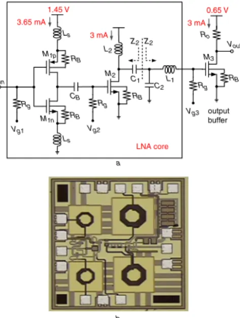
The 3 – 10 GHz UWB LNA fabricated by 0.18 mm TSMC CMOS process is shown inFig. 3. It is known that maximum power transfer will occur by means of conjugate impedance matching. The inter-stage resonator (C2, L1) in Fig. 3accomplishes bandwidth extension
owing to the conjugate impedance matching.Fig. 4shows the simulated impedances of Z1(solid line) and Z2(dashed line) (seeFig. 3a) from 4 to
12 GHz. The best conjugate impedance matching is designed near 9.6 GHz by using the inter-stage resonator to improve the bandwidth without additional power consumption. In addition, a larger substrate resistor RB is adopted in the RF MOS device to obstruct undesired
noise power from the substrate port, and the buffer transistor M3with
a 50 V resistive load Roin the proposed UWB LNA is employed to
achieve output matching for testing purposes.
a LNA core 3.65 mA Vg1 Vg2 Vg3 Vout output buffer M1p M1n M2 M3 L2 L1 Z2Z2 C1 C2 Rg RB Rg RB Rg Ro RB Ls Ls RB CB Vin 1.45 V 0.65 V 3 mA 3 mA b
Fig. 3 Complete schematic and die microphotograph of proposed UWB LNA a Complete schematic
b Die microphotograph
Z2
Z1
conjugate impedance matching at 9.6 GHz
4–12 GHz
Fig. 4 Input reflection coefficients on Smith chart for impedances Z1(solid
line) and Z2(dashed line) shown inFig. 3a
Results: The UWB LNA chip is measured by on-wafer probing and the total DC core power dissipation is 6.8 mW. A die microphotograph of the fabricated LNA is shown in Fig. 3b, with a die area including pads of 0.81× 0.81 mm2. The S-parameters of the designed LNA are
measured using an Agilent E8361A PNA network analyser. The noise figure (NF) is measured using an Agilent N8975A noise figure analyser with Agilent 346C noise source. Simulated and measured results of power gain and input return loss are depicted in Fig. 5. The small signal peak gain is 16.2 dB with 3 dB bandwidth of 7 GHz from 3 to 10 GHz and input return loss is better than 10 dB in the operation band-width. The simulated and measured noise figure at the same bias con-dition is also depicted inFig. 5. It is seen that the minimum value of NF is equal to 2.3 dB at 3.5 GHz. The proposed LNA performance is compared with recently published CMOS LNAs and summarised in
Table 1[4 – 8]. 3 4 5 6 7 8 9 10 11 0 1 2 3 4 5 6 S11 S21 NF measurement simulation frequency, GHz noise figure, dB –15 –10 –5 0 5 10 15 S21 and S 11 , dB
Fig. 5 Measured S-parameters and noise figure of proposed UWB LNA
Table 1: UWB LNA performance summary
Ref. Tech.!(mm) (GHz)BW G(dB)max NF(dB)min (mW)Pdiss (mmArea2
) ∗FOM/Area [1] 0.13 0 – 12.1 18.7 3 27.6 0.88 4.29 [2] 0.18 3 – 4.8 13.9 4.7 14.6 0.95 0.33 [3] 0.13 2.2 – 9 11.3 3.9 30 0.68 0.87 [4] 0.18 2 – 12 11.8 3.1 22.7 0.45 3.66 [5] 0.13 0.1 – 10 17 5.3 60 0.64 0.76 [6] 0.13 3 – 10.35 12.5 3.3 7.2 0.77 4.92 [7]+ 0.13 4.7 – 11.7 12.4 2.9 13.5 – – [8] 0.18 0 – 16 10 3.6 21 1.19 1.57 TW 0.18 3 – 10 16.2 2.3 6.8 0.66 14.4
+ simulation results ! CMOS ∗
FOM= BW[GHz] Gmax[lin] (NFmin[lin]−1) Pdiss[mW] Area[mm2]
Conclusion: The UWB LNA with a new input-matching concept has been fabricated by using 0.18 mm CMOS process. A superior noise performance with easily be achieved by the usage of the proposed induc-torless input-matching technique. The inter-stage resonator is employed for low power application to accomplish gain bandwidth extension without extra DC power dissipation.
Acknowledgment: The authors thank the Chip Implementation Center (CIC) for technical support.
#The Institution of Engineering and Technology 2010 11 May 2010
doi: 10.1049/el.2010.1279
One or more of the Figures in this Letter are available in colour online. C.-P. Liang, C.-W. Huang, Y.-K. Lin and S.-J. Chung (Department of Communication Engineering, National Chiao Tung University, Hsinchu 300, Taiwan)
E-mail: sjchung@cm.nctu.edu.tw References
1 Chang, J.-F., and Lin, Y.-S.: ‘3-10 GHz low-power low-noise CMOS distributed amplifier using splitting-load inductive peaking and noise-suppression techniques’, Electron. Lett., 2009, 45, (9), pp. 1033– 1035 2 Jeong, M.l., Lee, J.N., and Lee, C.S.: ‘Design of UWB switched gain
controlled LNA using 0.18 mm CMOS’, Electron. Lett., 2008, 44, (3), pp. 477 – 478
3 Nguyen, G.D., Cimino, K., and Feng, M.: ‘A RF CMOS amplifier with optimized gain, noise, linearity and return losses for UWB applications’. IEEE Radio Frequency Integrated Circuit Symp., Atlanta, GA, USA, June 2008, pp. 505 – 508
4 Chen, C.-C., Lee, J.-H., Lin, Y.-S., Chen, C.-Z., Huang, G.-W., and Lu, S-S.: ‘Low noise-figure P+ AA mesh inductors for CMOS UWB RFIC applications’, IEEE Trans. Electron Devices, 2008, 55, (12), pp. 3542 – 3548
5 Wu, T.-H., Syu, J.-S., and Meng, C.-C.: ‘Analysis and design of the 0.13-Mm CMOS shunt-series series-shunt dual-feedback amplifier’, IEEE Trans. Circuits Syst. I, Reg. Pprs, 2009, 56, (11), pp. 2373 – 2383 6 Wu, C.-Y., Lo, Y.-K., and Chen, M.-C.: ‘A 3-10 GHz CMOS UWB
low-noise amplifier with ESD protection circuits’, IEEE Microw. Wirel. Compon. Lett., 2009, 19, (11), pp. 737 – 739
7 Mirvakili, A., and Yavari, M.: ‘A noise-canceling CMOS LNA design for the upper band of UWB DS-CDMA receivers’. IEEE Int. Symp. on Circuits and Systems, Taipei, Taiwan, May 2009, pp. 217 – 220 8 Entesari, K., Tavakoli, A.R., and Helmy, A.: ‘CMOS distributed
amplifiers with extended flat bandwidth and improved input matching using gate line with coupled inductors’, IEEE Trans. Microw. Theory Tech., 2009, 57, (12), pp. 2862 – 2871