行政院國家科學委員會專題研究計畫 期中進度報告
金屬閘極/高介電係數材料互補式金氧半場效電晶體在 45
到 22 奈米世代之應用(2/3)
期中進度報告(精簡版)
計 畫 類 別 : 整合型
計 畫 編 號 : NSC 98-2120-M-009-005-
執 行 期 間 : 98 年 08 月 01 日至 99 年 07 月 31 日
執 行 單 位 : 國立交通大學電子工程學系及電子研究所
計 畫 主 持 人 : 荊鳳德
共 同 主 持 人 : 管傑雄、張廖貴術、王水進、巫勇賢
報 告 附 件 : 出席國際會議研究心得報告及發表論文
處 理 方 式 : 本計畫可公開查詢
中 華 民 國 99 年 05 月 17 日
行政院國家科學委員會補助專題研究計畫
□ 成 果 報 告
■期中進度報告
金屬閘極/高介電係數材料互補式金氧半場效電晶體在 45 到 22 奈米世代
之應用(2/3)
計畫類別:□ 個別型計畫 ■ 整合型計畫
計畫編號:NSC 98-2120-M-009-005
執行期間: 2009 年 8 月 1 日至 2010 年 7 月 31 日
計畫主持人:荊鳳德教授(國立交通大學電子工程學系及電子研究所)
共同主持人:管傑雄教授(國立臺灣大學電子工程學研究所)
張廖貴術教授(國立臺灣大學工程與系)
巫勇賢助理教授(國立臺灣大學工程與系統科學系)
王水進教授(國立成功大學微電子工程研究所)
計畫參與人員:陳維邦、周坤億、蔡竣揚、劉思麟
成果報告類型(依經費核定清單規定繳交):■精簡報告 □完整報告
本成果報告包括以下應繳交之附件:
□赴國外出差或研習心得報告一份
□赴大陸地區出差或研習心得報告一份
□出席國際學術會議心得報告及發表之論文各一份
□國際合作研究計畫國外研究報告書一份
處理方式:除產學合作研究計畫、提升產業技術及人才培育研究計畫、列管計
畫及下列情形者外,得立即公開查詢
□涉及專利或其他智慧財產權,□一年□二年後可公開查詢
執行單位:國立交通大學電子工程學系及電子研究所
中 華 民 國 99 年 5 月 12 日
金屬閘極/高介電係數材料互補式金氧半場效電晶體在45到22奈米世代之應用(2/3)
“Metal-gate/ high-κ CMOSFETs for 45 to 22 nm technology nodes”
計畫編號:NSC 98-2120-M-009-005
執行期間:98 年 08 月 01 日至 99 年 07 月 31 日
主持人:荊鳳德 交通大學電子工程系教授
一、 中文摘要
高的「臨界電壓」(Vt)是「金屬閘極/高介電係數」 互補式「金氧半場效電晶體」的主要挑戰,我們發現了 較高的「臨界電壓」主要是由於在小的「等效氧化層厚 度」(EOT)下「平帶電壓」(Vfb)下降所導致。而「平帶 電壓」的下降,其物理機制為帶電的氧缺陷在界面上反 應所產生。我們利用先進的低溫製程來降低界面反應的 問題。利用此方法,在「自我對準」和「閘極優先」的 互補式「金氧半場效電晶體」上,可以在「等效氧化層 厚度」0.6~0.7 奈米時達到低的0.12 and -0.17 V「臨界 電壓」。二、 英文摘要
The toughest challenge for metal-gate/high-κ CMOS
is to lower the undesired high threshold voltage (Vt) at
smaller equivalent-oxide thickness (EOT) [1]-[9], which is
opposite to scaling trend of low power ICs. The high Vt
issue is especially hard for p-MOS, since only Ir and Pt in the Periodic Table have the needed high work-function larger than the target 5.2 eV. Unfortunately, both Ir and Pt are not thermally stable on thin high-κ dielectric [1]. Further, the flat band (Vfb) roll-off at smaller EOT even
worsens the required low Vt challenge [6]-[7]. The tough
challenge is evident from the slower EOT scaling: 1.0 nm
EOT of Intel 1st-generation high-κ + metal-gate CMOS for
45 nm node (IEDM 2007) to only 0.95 nm EOT of
2nd-generation technology for 32 nm node (IEDM 2009).
To address these issues, in this paper we present possible mechanism for the high Vt issue from our experiment data, which is due to flat-band voltage (Vfb) roll-off at smaller EOT. A mechanism of charged oxygen vacancies formed
by interface reaction was proposed to explain the Vfb
roll-off effect. Based on this mechanism, a novel process
method has been used that leads to the low Vt
metal-gate/high-κ CMOSFETs at 0.6~0.7 nm EOT with several orders of magnitude lower gate leakage. Such small EOT is significantly smaller than the 0.95 nm EOT
used in Intel’s 2nd-generation high-κ + metal-gate CMOS
at 32 nm node.
二、 計畫的緣由與目的
A fundamental challenge for metal-gate/high-κ
C-MOSFETs is the undesirable high threshold voltage (Vt) that is opposite to low voltage scaling trend. This is especially difficult for high work-function p-MOS, since only Ir and Pt in the Periodic Table have the required high work-function greater than the target 5.2 eV. However, both Ir and Pt fail for p-MOS devices, due to metal diffusion through the high-κ dielectric during the 1000oC
RTA necessary for ion-implanted source-drain activation
[1]. Although thermal stability up to 1000oC can be
achieved by using an Ir3Si gate [4]-[5] on HfLaON
developed by us, this yields a Vt of only -0.1 V, at 1.6 nm equivalent-oxide-thickness (EOT). Unfortunately this value increases at a thinner EOT of 1.2 nm due to the roll-off of the flat-band voltage (Vfb) [6], as a result of reactions and inter-diffusion at the high-κ/Si interface. Although the interfacial reaction can be decreased by
inserting a thin SiO2 layer, this may not work when the
EOT is scaled down to ~0.7 nm. This is evident from the limited EOT scaling of 1.0 to 0.95 nm with down-scaling the technology from 45 to 32 nm nodes. Such negligible EOT scaling is much slower than the EOT proposed by
International Technology Roadmap for Semiconductors
(ITRS). Since the inevitable interfacial reactions follow an Arrhenius temperature dependence, low-temperature processing is essential. This has been verified by the low
Vt in metal-gate/high-κ p-MOSFETs in our previous works
when a < 900oC solid-phase diffusion (SPD) was used to
form the ultra-shallow junctions [6] and laser-annealing of the laser-reflective-gated CMOS with an EOT in the range 1.05~1.2 nm [7].
To address these issues, in this paper we present a possible mechanism of Vfb roll-off effect at smaller EOT – the charged oxygen vacancies generated by interface reaction. Based on the proposed mechanism, we have developed a low temperature process for metal-gate/high-κ CMOS silicide-induced doping for source-drain shallow junction. The fabricated metal-gate/high-κ CMOSFETs using this method have good control of Vfb roll-off with
low Vt values of 0.12 and -0.17 V at small 0.6~0.7 nm
than poly-Si/SiO2 stack at the same EOT. Such good
transistor performance further supports our proposed mechanism of Vfb roll-off effect.
三、 研究方法及成果
A. Experimental procedure:
Standard Si wafers with ~10 ohm-cm resistivity were used in this study. To increase the κ value, we added higher κ TiO2 dielectric into our pioneered La2O3 [8]-[9].
The TiO concentration is ~25% as controlled by the calibrated thickness rate during LaTiO deposition. After depositing the high-κ gate dielectrics on Si substrate using physical vapor deposition (PVD), a post-deposition anneal (PDA) under O2 is applied to decrease the defects in gate
dielectric. Then different low and high work-function TaN and Ir metal-gates were deposited on high-κ dielectric using PVD and subsequent gate patterning for n- and
p-MOSFETs, respectively.
After gate patterning, self-aligned 20 nm or Sb 5 nm Ga and thin Ni were deposited for respective n- and
p-MOSFET, followed by silicide-induced doping at
600~650oC RTA and removing the non-reacted metals [6].
The Ni-induced SPD is similar to dopant segregation technique, where both cases use the silicidation to drive in the impurities. However, the impurities in dopant segregation technique were delivered by ion-implantation, while in Ni-induced SPD used the PVD deposited Ga and drive in [8]-[9]. The fabricated MOSFETs were characterized by capacitance-voltage (C-V) and current- density-voltage (J-V) measurements.
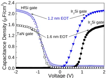
B. Interface reaction and Vfb roll-off at thinner EOT: Figure 1 shows the C-V characteristics of HfLaON CMOS. The adding La2O3 into HfO2 with nitridation can
achieve wanted negative Vfb in TaN/HfLaON n-MOS at
1.6 nm EOT, while needed positive Vfb is also reachable
using high work-function Ir3Si gate on HfLaON, even after
1000oC RTA. These results indicate the good V
fb control for n- and p-MOS in top metal-gate/high-κ interface. The nitridation is important for HfLaON to preserve an
amorphous structure at 1000oC RTA, where the HfLaO
starts to crystallize at RTA temperature above 900oC RTA.
However, as the EOT of HfLaON gate dielectric scaled down to 1.2 nm, severe Vfb roll-off was found using
the same Ir3Si metal-gate on HfLaON gate dielectric.
Although negative Vfb was still obtained for n-MOS using
lower work-function HfSi2-x gate on HfLaON gate
dielectric, no proper work-function metal-gate can be used
for p-MOS under the requirement of 1000oC RTA for
process integration. -2 -1 0 1 2 0.0 0.4 0.8 1.2 1.6 2.0 2.4 1.2 nm EOT TaN gate HfSi gate Ir3Si gate Voltage (V) C apacitance Density
(
μ F/c m 2)
Ir3Si gate 1.6 nm EOTFig. 1. C-V characteristics of mixed high-κ HfLaON n- and
p-MOS capacitors with various metal-gates after 1000oC
RTA. The Vfb roll-off is found at smaller EOT.
To analyze the Vfb roll-off effect from 1.6 nm to 1.2 nm EOT, we have examined the Vfb dependence. The Vfb is related to the fixed oxide charges (Qf), distributed oxide
chargesρox(x)), work-function difference between
metal-gate and Si (ΦMS= ΦM-ΦS), and Vt:
∫
− − Φ = t x ox ox ox ox f MS fb x dx x x C C Q V 0 0 ( ) 1ρ
(1) Vt = Vfb + 2ϕF + Qdep/Cox (2)Here Cox is the gate capacitance, Qdep is the depletion
charge and 2ϕF is the surface potential bending at onset of
charge inversion. Since the same Ir3Si/HfLaON gate stack
and 1000oC thermal cycle were used, the V
fb roll-off at thinner EOT is unlikely from the top metal/high-κ interface or ΦM difference. The ϕF, ΦS and Qdep depend
strongly on the doping concentration of Si, which is also kept the same when scaling down the EOT. Therefore, the
Vfb roll-off at thinner EOT is due to oxide charges and/or dipoles from the above equation.
Here we propose that the oxide charges at thinner EOT are generated from interface reaction at high temperature: x x HfO SiO HfO Si+ 2⎯⎯→Δ + 2− (3)
Such interface reaction, generating oxygen vacancy charges of non-stoichiometric SiOx and HfO2-x (x<2), is
inevitable at 1000oC RTA due to the close bond enthalpy
of SiO2 (800 kJ/mol) and HfO2 (802 kJ/mol) [1]. Here
the bond enthalpy is defined as the standard molar enthalpy change of bond dissociation. From the interface reaction and Vfb roll-off effect at thinner EOT, the bottom high-κ/Si interface is also the key factor for low Vt CMOS.
C. Solution - silicide-induced doping for source-drain
shallow junction:
To further investigate our proposed Vfb roll-off effect by interface reaction, we have measured RTA temperature dependence on C-V characteristics of higher κ TaN/LaTiO
p-MOS capacitors under different 600~900oC temperature.
As shown in Fig. 2, the Vfb roll-off increases with
increasing RTA temperature from 600 to 900oC. In
addition, a degraded EOT is also found with increasing RTA temperature.
We have used cross-sectional TEM to analyze the EOT degradation with increasing RTA temperature. As shown in Fig. 3, the degraded EOT is due to the forming thicker interfacial oxide layer as observed by cross-sectional TEM. These results were predicted by the
Vfb roll-off mechanism proposed in eq(1)- eq(3), which is also srelated to the interface reaction trongly. Besides, the
Vfb roll-off effect can also be decreased by decreasing
process temperature. -2 -1 0 1 0 1 2 3 4 900oC EOT=0.72nm V fb=-0.27V CVC Fitting QMCV Fitting 800oC EOT=0.73nm V fb=-0.4V Voltage (V) Cap a citan c e Densi ty
(
μ F/cm 2)
600oC EOT=0.63nm V fb=-0.52VFig. 2. The PDA temperature dependence on C–V characteristics of TaN/LaTiO/p-Si n-MOS devices. The
600oC C–V data were measured in a MOSFET from
accumulation to inversion, while the 800oC and 900oC
C–V data were measured in MOS capacitors from
accumulation to depletion. 5 nm TaN Si LaTiO 5 nm TaN Si LaTiO 5 nm TaN Si LaTiO (a) (b)
Fig. 3. The cross-sectional TEM pictures of
TaN/LaTiO/p-Si n-MOS devices after 600oC and 900oC
RTA.
Using the low temperature process of 600~650oC and
high work-function Ir gate metals, we have also fabricated the Ir/LaTiO p-MOS capacitors, in additional to the TaN/LaTiO n-MOS capacitors in Fig. 2. As shown in the
C-V characteristics of Fig. 4, proper positive Vfb value with small hysteresis is still obtained even at small EOT of 0.66 nm for p-MOS capacitors.
It is important to notice that the different EOT value between n- and p-MOS devices is due to the process variation and the different electron and hole effective mass and wave-function distribution, from quantum-mechanical
C-V calculation. -1 0 1 2 0 1 2 3 4 EOT = 0.66 nm Voltage (V) Capa citance D ensity ( μF/ cm 2 )
TaN / Ir / TiLaO / n-Si
From +3 V to -1 V From -1 V to +3 V QM C-V simulation
Fig. 4. [TaN-TaN/Ir]/LaTiO p-MOS capacitors.
However, the challenge is how to fabricate the MOSFET at low temperature. Conventionally, a high
temperature RTA of 1000oC is required to activate
ion-implanted dopants in the source-drain of a MOSFET. The other methods to dope the source-drain at low temperature are the solid-phase diffusion [6] and silicide-induced doping [8]-[9]. Here we used silicide-induced doping to fabricate the CMOS devices since it has even lower process temperature than using solid-phase diffusion.
Figures 5(a) and 5(b) show the transistor Id-Vg
characteristics of self-aligned and gate-first TaN/LaTiO n- MOSFETs and Ir/LaTiO p-MOSFETs, respectively. Low
Vt of -0.17 and 0.12 V were reached at these small EOT of 0.63 and 0.66 nm for n- and p-MOSFETs, respectively. These excellent results are due to the using higher κ LaTiO
gate dielectric and low temperature (600~650oC)
NiSi-induced doping in source-drain. Such small EOT is significantly smaller than the 0.95 nm EOT used in Intel’s
2nd-generation high-κ + metal-gate CMOS at 32 nm node
(IEDM 2009). These results further support our proposed interface reaction mechanism with its Arrhenius temperature dependence.
-2.0 -1.5 -1.0 -0.5 0.0 0.5 1.0 10-10 10-8 10-6 10-4 VT = - 0.17 V
TaN / Ir / TiLaO / n-Si
Vd = - 0.1 V D rain Current (A ) Gate Voltage (V) (a) -1.0 -0.5 0.0 0.5 1.0 1.5 2.0 10-10 10-8 10-6 10-4 10-2 Drain current Gate current Vd = 0.1 V Dr a in Cu rr e n t ( A ) Gate Voltage (V) TaN/TiLaO/p-Si VT=0.12 V (b)
Fig.5 Id-Vg characteristics of self-aligned and gate-first (a) TaN/LaTiO n- MOSFETs and (b) Ir/LaTiO p-MOSFETs.
四、
結論與討論We have analyzed the Vfb roll-off effect at smaller
EOT and proposed a mechanism of charged oxygen vacancies by interface reaction for the explanation. The interface reaction can also be decreased by using novel low temperature process from its Arrhenius temperature dependence. Using a simple process, we have fabricated
metal-gate/high-κ TaN/LaTiO n-MOSFET with a low Vt
of 0.12 V at 0.63 nm EOT and Ir/LaTiO p-MOSFET with
a low Vt of -0.17 V at 0.66 nm EOT. Besides, this device
has the advantages of simple self-aligned and gate-first process compatible with current VLSI.
五、Reference
[1]. D. S. Yu, Albert Chin, C. H. Wu, M.-F. Li, C. Zhu, S. J. Wang, W. J. Yoo, B. F. Hung and S. P. McAlister, “Lanthanide and Ir-based dual metal-gate/HfAlON CMOS with large work-function difference,” in IEDM Tech. Dig., 2005, pp. 649-652.
[2]. C. H. Wu, D. S. Yu, Albert Chin, S. J. Wang, M.-F. Li, C.
Zhu, B. F. Hung, and S. P. McAlister, “High work function IrxSi
gates on HfAlON p-MOSFETs,” IEEE Electron Device Lett. 27, no. 2, pp. 90-92, 2006.
[3]. X. P. Wang, C. Shen, M.-F. Li, H. Y. Yu, Y. Sun, Y. P. Feng, A. Lim, H. W. Sik, A. Chin, Y. C. Yeo, P. Lo, and D. L. Kwong, “Dual metal gates with band-edge work functions on novel HfLaO high-κ gate dielectric,” in Symp. VLSI Tech. Dig., 2006, pp. 12-13.
[4]. C. H. Wu, B. F. Hung, Albert Chin, S. J. Wang, X. P. Wang, M.-F. Li, C. Zhu, Y. Jin, H. J. Tao, S. C. Chen, and M. S. Liang
“High temperature stable [Ir3Si-TaN]/HfLaON CMOS with large
work-function difference,” in IEDM Tech. Dig., 2006, pp. 617-620.
[5]. B. F. Hung, C. H. Wu, Albert Chin, S. J. Wang, F. Y. Yen, Y. T. Hou, Y. Jin, H. J. Tao, S. C. Chen, and M. S. Liang, “High
Temperature Stable IrxSi Gates with High Work Function on
HfSiON p-MOSFETs,” IEEE Trans. Electron Device, vol. 54, no. 2, pp. 257-261, 2007.
[6]. C. F. Cheng, C. H. Wu, N. C. Su, S. J. Wang, S. P. McAlister
and Albert Chin, “Very low Vt [Ir-Hf]/HfLaO CMOS using novel
self-aligned low temperature shallow junctions,” in IEDM Tech.
Dig., 2007, pp. 333-336.
[7]. C. C. Liao, Albert Chin, N. C. Su, M.-F. Li, and S. J. Wang,
“Low Vt gate-first Al/TaN/[Ir3Si-HfSi2-x]/HfLaON CMOS using
simple process,” in Symp. on VLSI Tech. Dig., 2008, pp. 190-191. [8]. S. H. Lin, C. H. Cheng, W. B. Chen, F. S. Yeh, and Albert Chin, “Low Threshold Voltage TaN/Ir/LaTiO p-MOSFETs Incorporating Low-Temperature-Formed Shallow Junctions,”
IEEE Electron Device Lett., vol. 30, pp. 681-683, June 2009.
[9]. S. H. Lin, C. H. Cheng, W. B. Chen, F. S. Yeh, and Albert Chin, “Low Threshold Voltage TaN/LaTiO n-MOSFETs with Small EOT,” IEEE Electron Device Lett., vol. 30, pp. 999-1001, Sept. 2009.
六、
Invited Papers (List from Aug. 2009~May 2010)
[1] Albert Chin, M. F. Chang, S. H. Lin, W. B. Chen, P. T. Lee, F. S. Yeh, C. C. Liao, M.-F. L, N. C. Su and S. J. Wang “Flat
Band Voltage Control on Low Vt Metal-Gate/High-k
CMOSFETs with small EOT,” 16th Bi-Annual Conference on
Insulating Films on Semiconductors (INFOS), pp. 1728–1732,
Cambridge University, UK, June 29~July 1, 2009. (Invited)
[2] Albert Chin, S. H. Lin, K. C. Chiang, and F. S. Yeh, “Improved Device Characteristics in Charge-Trapping-
Engineered Flash Memory Using High-k Dielectrics,” 7th Intl.
Symp. on High Dielectric Constant Materials and Gate Stacks,
216th Electro Chemical Society (ECS) Meeting, Vienna, Austria,
Oct. 2009. (Invited & Session Chair)
[3] Albert Chin, “Charge-trapping memories: materials and devices,” Materials Research Society (MRS), San Francisco,
USA, April 2010. (Tutorial & Section Chair)
[4] Albert Chin, “Novel Ultra-Low Energy High-Speed Non-Volatile Memory with Good Retention and Endurance,” CMOS Emerging Technologies, Whistler, BC, Canada, May