鎳矽化物應用在奈米金氧半導體元件技術之研究
176
0
0
全文
(2) 鎳矽化物應用在奈米金氧半導體元件技術之研究. 研究生:李宗霖. 指導教授:李崇仁 博士 雷添福 博士. 國立交通大學. 電子工程學系. 電子研究所. 摘要. 在先進互補式金氧半導體元件裡,當接觸尺寸縮小至奈米等級,源極及汲極 的接觸電阻也會隨之增加。因此,金屬矽化物的技術應用在源極及汲極已經被開 發用來同時降低接觸電阻及接面寄生電阻。在奈米金氧半場效電晶體的製造中, 矽化製程是必須的,為了抑制源極及汲極的超淺接面形成所產生的短通道效應。 所以,是否具有與矽基材完好介面特性的金屬矽化物,是在製造奈米尺寸的元件 時重要的製程考量。除此之外,當閘極氧化層隨著元件尺寸縮小而縮小時,閘極 金屬矽化的製程,是否會對閘極氧化層可靠度造成影響也是一個需要考量的因 素。 在本論文中,主要研究的方向是,鎳矽化物與超淺接面製程、完全閘極金屬 矽化製程整合的可靠度研究。首先,我們對鋯覆蓋在鎳上後形成的金屬矽化物的 熱穩定性作一系列的研究。藉由鋯在金屬矽化過程中,抑制氧摻雜的能力,鎳矽 化物的熱穩定性將能大大的改善。並且由穿隧式電子顯微鏡的觀測,這種方法能 獲得一個平緩的矽化物與矽的介面。 然後,我們將蓋有鋯的鎳堆疊在二極體接面後形成鎳矽化物,研究用鋯覆蓋 的方法對鎳矽化接面特性的影響,並與傳統用鈦覆蓋的方法作一個比較。由於熱 穩定性上的改善,經由金屬矽化過程所造成的接面漏電增加,果然如預期的被抑 i.
(3) 制。並由於矽化物深度良好控制的優點,鎳矽化物形成在 30 奈米深的超淺接面 上也如預期般的被實現了。 再者,我們對利用 PH3 電漿摻雜方式所形成的超淺接面,作一個探討。雖然 表面雜質濃度低的缺點,能藉由一個覆蓋層來改善,但同時也造成了接面深度的 增加。在我們的實驗中,我們發現,在 PH3 電漿摻雜後,透過短時間的退火的 方式,能形成一個較少缺陷的超淺接面。 最後,我們去觀察在鎳矽化物形成在不同閘極結構上的特性。經於磷的摻雜, 能增加閘極氧化層的可靠度。因此,我們相信,對於應用在未來元件製作上,完 全鎳矽化閘極仍具有潛力。. ii.
(4) Investigation of Nickel Silicide Application toward Nano-Scale MOS Device Technology Student: Tsung Lin Lee. Advisors: Dr. Chung Len Lee Dr. Tan Fu Lei. Department of Electronics Engineering & Institute of Electronics National Chiao-Tung University. Abstract. In advanced CMOS devices, as contact dimensions scale down to nanometer range, contact resistance of source and drain is increased correspondingly. As a result, the technique of metal silicides for poly gate and source/drain has been developed to reduce the contact resistance and the parasitic junction resistance as well. In nanometer MOSFET fabrication, this silicidation process requires considering to suppress short channel effect (SCE) when forming the ultra shallow source and drain junction. Therefore, metal silicides owning a perfect interfacial property with Si above an ultra-shallow junction is considered as a critical module toward the realization of nano-scale CMOS. Besides, as the oxide thickness scaling down with the device dimensions, the gate oxide reliability will also be a concern for the silicided gate process. The objective of this dissertation is to investigate the feasibility of nickel silicide integration into the formation process of the ultra shallow junction and full silicide iii.
(5) gate. First of all, we have investigated the thermal stability of nickel silicide with Zr capping. To employ its good capability for the suppression of oxygen incorporation during silicidation process, a siginificantly improvement on the thermal stability of nickel silicide can be obtained. And a smooth interface between silicide and silicon also can be demonstrated by TEM images. Then, we combined the Zr capped on nickel silicide with the p+/n junction, and investigated the influence on junction charateristics by this capping layer compared with a conventional Ti-capped method. Due to the advantages of improvement on thermal stability, the increase of leakage current resulted from the silicidation process can be suppressed as expected. By the advantage of well-controlled silicide depth, an 30nm ultra shallow junction with nickel silicide was also accomplished as expected. Third, the formation of ultra shallow junction by PH3 plasma doped method was investigated. Its low surface concentration can be improved by a cap layer but meanwhile it will result in the increase of junction depth. In our experimental, a defect less ultra shallow junction formation by PH3 plasma doped can be achieved by short activation time. Finally, we have observed the behavior of nickel silicide gate based on different gate structures. By phosphorus incorporation, the gate oxide reliability can be enhanced. Thus, we believed that full nickel silicide gate still possesses potential for the application on future device fabrication.. iv.
(6) 誌謝 本論文的完成,首先要感謝我的指導老師李崇仁教授及雷添福教授,感謝他 們在這段研究期間的指導與勉勵,細心地為我解答在研究上所發生的問題,並給 予適當的建議;除了讓我順利克服研究瓶頸,也幫助我學習到正確研究學問的態 度與方法,李老師和雷老師嚴謹的研究精神及圓融的處事態度讓我終身受益。另 外還要感謝指導我的學長李介文博士,對於研究上的啟發,並幫助我培養獨立研 究的能力;此外,也要特別感謝李名鎮學長在量測上給予我的大力幫助。 我還要感謝實驗室裡的學長、同學、學弟妹們:張子云學長,哲麒、明山、 建豪、世豪、信強、育賢、凰君、德慶、獻德、柏儀、紹明、美錡、松齡、韋翔、 國誠、余俊、任逸和家文等人,帶給我溫馨快樂的時光;同時也要特別感謝與我 一同研究的學弟妹們:美錡、久盟及志仰,在研究上互相討論及專業知識的相互 成長,還有實驗時的鼎力相助。 此外,我還要感謝彭作煌先生對於計測實驗室管理維護上的幫助、助理陳秋 雲小姐、吳淑敏小姐和小姐的鼓勵;另外我還要感謝半導體中心(奈米中心)裡 的工作人員:彭兆光先生、徐秀鑾小姐、林素珠小姐、黃月美小姐、范秀蘭小姐、 陳悅婷小姐、徐台鳳小姐、何惟美小姐、楊月嬌小姐及胡進章先生等人,謝謝你 們在這段日子裡,在實驗過程中的幫助,讓我的論文順利完成,也同時給予我難 以忘懷的實驗室回憶。 最後,我要特別感謝我的父母、哥哥、妹妹、叔叔、舅舅等親朋好友在背後 的全力支持與鼓勵,讓我能毫無後顧之憂的在研究道路上全力衝刺,並且也要感 謝我的女友淑敏及其家人,對於我的鼓舞及支持。 願將此論文獻給所有關心我的人。. v.
(7) CONTENTS ABSTRACT (in Chinese)…………………………………………………………..i ABSTRACT (in English)…………………………………………...….....iii ACKNOWLEDGEMENTS……………………………………...……. v CONTENTS……………………………………………………...……….vi TABLE CAPTIONS…………………………………………………...…………...x FIGURE CAPTIONS……………………………………………………………..xii. Chapter 1 Introduction………………………………………………...……..….1 1.1 Background……………………………………………………………………...…1 1.2 Motivation………………………………………………………………...…….....3 1.3 Organization of the Thesis…………………………………..……………………..4. Chapter 2 Characteristics of Nickel Silicide with a Zirconium Cap Layer………………………........…………………………………...…6 2.1 Introduction……………………………………………………...………………...6 2.2 Experimental……………………………………………………………...…….....7 2.3 Results and Discussion……………………...……………………………………...……8 2.3.1 Sheet Rsistance of Nickel Silicide on n-type Si/p-type Si…………………..8 2.3.2 XRD Analysis for Zr capped on Nickel Silicide……………………….....…9 2.3.3 TEM Image for Zr capped on Nickel Silicide……………………………...…10 2.4 Summary………………………………………………………...…….…...………..…..10. vi.
(8) + Chapter 3 Characteristics of Nickel Silicide on P /N Junction. Combined with a Zirconium Cap Layer...………..…….........19 3.1 Introduction……………………………………………………...………...……..19 3.2 Experimental……………………………………………………………...………20 3.3 Results and Discussion……………………...………………………………...….22 3.3.1 SIMS Analysis for Nickel Silicided Junction with / without a Cap Layer…..22 3.3.2 Basic IV Characteristics of P+/N Nickel-Silicided Junction…….…...............23 3.3.3 Temperature Effects of P+/N Nickel Silicided Junction..................................24 3.4 Summary………………………………………………………...…….…...……..25. Chapter 4 Ultra-Shallow Junction Formation by PH3 Plasma Immersion Method…………………………………..….…..……..47 4.1 Introduction…………………………………………………………………...….47 4.2 Experimental……………………………...………………………………………48 4.3 Results and Discussion……………………………………...……………...…….49 4.3.1 Sheet Resistance and SIMS Analysis of PH3-Plasma Immersion Junction.…49 4.3.2 Basic IV Charateristics of PH3 Plasma Doped Junction.....………………......50 4.3.3 Temperature Effects of PH3 Plasma Doped Junction………………………......51 4.4 Summary………………………...………………………………………………..52. Chapter 5 Ultra shallow Junction Combined with Zirconium Capped Nickel Silicide…………….................................................................72 5.1 Introduction……………………………………...…………………………...…..72. vii.
(9) 5.2 Experimental………………………...……………………………………………73 5.3 Results and Discussion…………………...……………………………...……….75 5.3.1 Sheet resistance and SIMS profile of Nickel Silicided Ultra Shallow Junction…………………………………………………………………........75 5.3.2 Characteristics of Ultra Shallow Junction Combined with Nickel Silicide…………………………………………………..………............…...76 5.4 Summary……………………………...…………………………………………..77. Chapter 6 Characteristics of Full Nickel Silicide Gate Based on In-Situ Doped Amorphorus-Si and Amorphorus-Si / Poly-Si Stack Structure……………………….………………..…93 6.1 Introduction…………………………………………...………………………..93 6.2 Experimental………………………...………………………………………….94 6.2.1 Full Nickel Silicide Gate Based on In-Situ Doped and Undoped a-Si….....94 6.2.2 Full Nickel Silicide Gate Based on Stack Structure……...………………....95 6.2.3 Full Nickel Silicide Gate Based on In-Situ Doped a-Si with Zr Capping…..97 6.3 Results and Discussion……...………………………………………………....98 6.3.1 Characteristics of Full Nickel Silicide Gate Based on In-Situ Doped and undoped a-Si……………………………………………………………….98 6.3.2 Characteristics of Full Nickel Silicide Gate Based on Stack Structure….…101 6.3.3 Characteristics of Full Nickel Silicide Gate Based on In-Situ Doped a-Si With Zr Capping…………………………………………………...……….103 6.4 Summary………………………………………………………………………...104. viii.
(10) Chapter 7 Conclusions and Recommendations for Future Works…143 7.1 Conclusions………………………...…………………………………………143 7.2 Recommendations for Future Works…………………...………………...……..145. References…………………………………………………………………………..146 Vita…………………………………………………………………………...………154 Publication List…………………………………………………………...………155. ix.
(11) Table Captions Chapter 2 Table 2.1 Three different groups of samples were designed as : groupI : Ni/Si、 groupII : Ti/Ni/Si、groupIII : Zr/Ni/Si. Ni film is 10nm and 30nm, respectively and the capping layer is 5nm and 10nm, respectively on both n-type and p-type Si. Chapter 3 Table 3.1 P+/n junctions implanted by BF2 with and without nickel silicide in different capping conditions. The nickel film and the capping layer are about 10nm and 5nm respectively. Chapter 4 Table 4.1 the trend of S/D extension from ITRS99 Table 4.2 the split of different annealing conditions for ultra shallow junction formation by PH3 plasma immersion method Table 4.3 the electrical characteristics of PH3 plasma doped junction at 50W RF power for 5 minutes with different activation conditions. Chapter 5 Table 5.1 n+/p junction formation by PH3 plasma immersion with and without nickel silicide in different capping conditions. The nickel and the capping layer are about 10nm and 5nm respectively.. Chapter 6 Table 6.1 characteristics of full nickel silicide gate capacitors based on undoped a-Si by various RTA conditions of (a) 35Å (b) 50Å (c) 75Å-thick SiO2 Table 6.2 characteristics of full nickel silicide gate capacitors based on in-situ doped a-Si by various RTA conditions of (a) 35Å (b) 50Å (c) 75Å-thick SiO2 Table 6.3 characteristics of full nickel silicide gate capacitors based on n+ a-Si/p-Si by various RTA conditions of (a) 35Å (b) 50Å (c) 75Å-thick SiO2 x.
(12) Table 6.4 characteristics of full nickel silicide gate capacitors based on p-Si/n+ a-Si by various RTA conditions of (a) 35Å (b) 50Å (c) 75Å-thick SiO2. Table 6.5 characteristics of full nickel silicide gate capacitors based on in-situ doped a-Si with Zr capping by various RTA conditions of (a) 35Å (b) 50Å (c) 75Å-thick SiO2 Table 6.6 Comparison of electrical characteristics with different gate structures and various oxide thickness at RTA 500oC and 800oC.. xi.
(13) Figure Captions Chapter 2 Fig. 2.1. Sheet resistance of nickel silicide with and without capping. (a) nickel thickness is 30nm and the capping layer is 10nm. (b) nickel thickness is 10nm and the capping layer is 5nm.. Fig. 2.2. Transmission electron microscopy (TEM) image of the as-deposited nickel film.. Fig. 2.3. Transmission electron microscopy (TEM) images of nickel silicide. (a) non-capped Ni samples after RTA at 650ºC. (b) non-capped Ni samples after RTA at 850ºC. (c) Ti capped Ni samples after RTA at 650ºC. (d) Ti capped Ni samples after RTA at 850ºC. (e) Zr capped Ni samples after RTA at 650ºC. (f) Zr capped Ni samples after RTA at 850ºC.. Fig. 2.4. X-ray diffraction spectra (XRD) of (a) Ti/Ni/Si and (b) Zr/Ni/Si contact systems after annealing at 650ºC and 850ºC respectively.. Chapter 3. Fig. 3.1 Process flow of the nickel silicided junction Fig. 3.2a SIMS profiles of impurities. The dopant activation and silicidation condition are 950ºC and 850ºC. (a) Boron redistribution before and after silicidation. Silicide depth is about 10nm, which is consistent with observation of TEM, and the junction depth is about 0.12µm. Fig. 3.2b (b) The diffusion of nickel after silicidation at 850ºC with different capping layers. Zr-capping shows a good capability in suppressing penetration of nickel.. Fig. 3.2c (c) Oxygen contamination in nickel silicide in different capping conditions. This contamination can be eliminated by a novel Zr-cap layer.. xii.
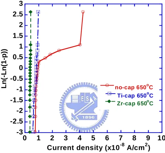
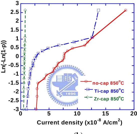
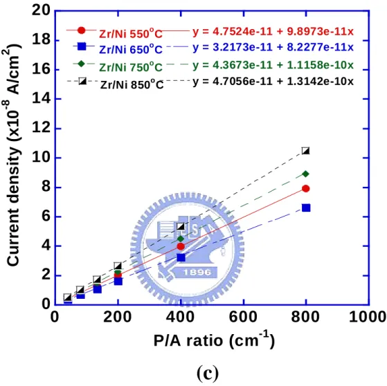
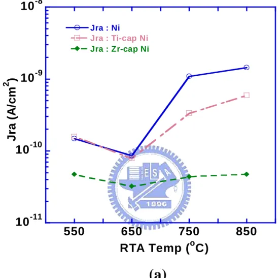
(14) Fig. 3.3 Reverse current-voltage characteristics of all groups at silicidation temperature of 650ºC and 850ºC. The size of the junction area is 1000×1000 µm2.. Fig. 3.4a Weibull plots of leakage current density measured at -3V for non-capped Ni samples at different RTA conditions. Fig. 3.4b Weibull plots of leakage current density measured at -3V for Ti capped Ni samples at different RTA conditions. Fig. 3.4c Weibull plots of leakage current density measured at -3V for Zr capped Ni samples at different RTA conditions.. Fig. 3.5a Weibull plots of leakage current density measured at -3V for all silicided samples. (a) at RTA condition of 650ºC Fig. 3.5b Weibull plots of leakage current density measured at -3V for all silicided samples. (a) at RTA condition of 850ºC. Fig. 3.6a. Comparison of the reverse junction leakage current density vs. the periphery to area ratio (P/A ratio) for (a) nickel silicide.. Fig. 3.6b Comparison of the reverse junction leakage current density vs. the periphery to area ratio (P/A ratio) for (b) Ti-capped nickel silicide. Fig. 3.6c Comparison of the reverse junction leakage current density vs. the periphery to area ratio (P/A ratio) for (c) Zr-capped nickel silicide. Fig. 3.7a (a) Reverse junction area leakage versus the RTA temperature for all nickdel silicided junctions in different capping conditions. Fig. 3.7b (b) Reverse junction periphery leakage versus the RTA temperature for all nickdel silicided junctions in different capping conditions.. xiii.
(15) Fig. 3.8 Reverse currrent voltage characteristics of non-capped Ni samples measured at various temperatures. (a) samples with RTA 650oC (b) samples with RTA 850oC. Fig. 3.9 Reverse currrent voltage characteristics of Ti capped Ni samples measured at various temperatures. (a) samples with RTA 650oC (b) samples with RTA 850oC. Fig. 3.10 Reverse currrent voltage characteristics of Zr capped Ni samples measured at various temperatures. (a) samples with RTA 650oC (b) samples with RTA 850oC. Fig.3.11a (a)Arrhenius plot (Ln IR/T3 versus 1/kT) for non-capped nickel silicide schottky junction after RTA at 650oC and 850oC, respectively measured at -3V. Fig.3.11b (b)Arrhenius plot (Ln IR/T3 versus 1/kT) for Ti capped nickel silicide schottky junction after RTA at 650oC and 850oC, respectively measured at -3V. Fig.3.11c (c)Arrhenius plot (Ln IR/T3 versus 1/kT) for Zr capped nickel silicide schottky junction after RTA at 650oC and 850oC, respectively measured at -3V.. Chapter 4 Fig. 4.1. (a) Key processes of n+/p junction formation. (b) The schematics of n+/p junction fabrication.. Fig. 4.2ab sheet resistance plot (a) with different Laser annealing energy. (b) with different Laser annealing engery and RTA at 950oC for 30s. Fig. 4.2c sheet resistance plot of the n+/p junction by PH3 plasma immersion with 100nm oxide capping (c) for different Laser energy Fig. 4.3. sheet resistance versus different RTA conditions. (a) both n+/p junction with and without oxide capping. (b) n+/p junction with oxide capping. xiv.
(16) Fig. 4.4a (a) sheet resistance versus different RTA conditions of n+/p junction with oxide capping by 50W plasma power for 1 minute. Fig. 4.4b (b) sheet resistance versus different RTA conditions of n+/p junction with oxide capping by 50W plasma power for 5 minutes. Fig. 4.4c (c) sheet resistance versus different RTA conditions of n+/p junction with oxide capping by 50W plasma power for 10 minutes. Fig. 4.5. SIMS profile of n+/p junction by PH3 plasma doping at various RTA temperatures (a) with (b) without oxide capping.. Fig. 4.6. (a) Reverse current-voltage characteristics of PH3 plasma junctions with different annealing conditions. (b) Weibull plots of reverse leakage current measured at 3V with different RTA conditions.. Fig. 4.7. Reverse junction leakage current density vs. periphery to area ratio (P/A ratio) with different annealing temperature for (a) 10s (b) 30s. Fig. 4.8. Mechanism of generation current ( a ) is at low reverse bias and ( b ) is at high reverse bias. Fig. 4.9 (a) Reverse currrent voltage characteristics measured at various temperatures of the junction with RTA 850oC for 30s. (b) Arrhenius plot (Ln IR/T3 versus 1/kT) of junction after RTA at 850oC, 30s measured at -3V. Fig. 4.10 (a) Reverse currrent voltage characteristics measured at various temperatures of the junction with RTA 900oC for 10s. (b) Arrhenius plot (Ln IR/T3 versus 1/kT) of junction after RTA at 900oC, 10s measured at -3V. Fig. 4.11 (a) Reverse currrent voltage characteristics measured at various temperatures of the junction with RTA 900oC for 30s. (b) Arrhenius plot (Ln IR/T3 versus 1/kT) of junction after RTA at 900oC, 30s measured at -3V. Fig. 4.12 (a) Reverse currrent voltage characteristics measured at various temperatures of the junction with RTA 950oC for 10s. (b) Arrhenius plot (Ln IR/T3 versus 1/kT) of junction after RTA at 950oC, 10s measured at -3V.. xv.
(17) Fig. 4.13 (a) Reverse currrent voltage characteristics measured at various temperatures of the junction with RTA 950oC for 30s. (b) Arrhenius plot (Ln IR/T3 versus 1/kT) of junction after RTA at 950oC, 30s measured at -3V. Fig. 4.14 (a) Reverse currrent voltage characteristics measured at various temperatures of the junction with RTA 1000oC for 10s. (b) Arrhenius plot (Ln IR/T3 versus 1/kT) of junction after RTA at 1000oC, 10s measured at -3V. Chapter 5 Fig. 5.1 (a) The simple process flow of n+/p silicided junction formation. (b) The schematics of n+/p silicided junction fabrication Fig. 5.2 Sheet resistance versus the annealing temperature for PH3 plasma junction. Fig. 5.3 SIMS profile of n+/p junction by PH3 plasma doping. The dopant activation condition is 950ºC for 10seconds. Fig. 5.4 Sheet resistance versus the silicidation condition for (1) Ni/Si (2) Ti/Ni/Si and (3) Zr/Ni/Si nickel silicide systems. Fig. 5.5 Reverse current-voltage characteristics of PH3 plasma junctions with and without nickel silicide. Fig. 5.6 Weibull plots of the leakage current of all nickel silicide samples at silicidation temperature of 650ºC and 850ºC respectively. And the size of junction area is 1000╳1000µm2. Fig. 5.7a (a) Cumulative leakage distribution for simple nickel silicided junction with the annealing temperature various from 550ºC to 850ºC. Fig. 5.7b (b) The weibull plot of leakage current density for nickel silicided junction with Ti capping after being annealed from 550ºC to 850ºC. Fig. 5.7c (c) Cumulative leakage distribution for Zr capped nickel silicided junction with the annealing temperature various from 550ºC to 850ºC.. xvi.
(18) Fig. 5.8a Comparison of reverse junction leakage current density vs. periphery to area ratio (P/A ratio) for (a) non-capped NiSi samples.. Fig. 5.8b Comparison of reverse junction leakage current density vs. periphery to area ratio (P/A ratio) for (b) Ti capped on NiSi samples. Fig. 5.8c Comparison of reverse junction leakage current density vs. periphery to area ratio (P/A ratio) for (c) Zr capped on NiSi samples. Fig. 5.9 Reverse junction (a) area leakage (b) periphery leakage versus the RTA temperature for all nickel silicide samples in different capping conditions. Chapter 6 Fig. 6.1 Key process flow and schematics of the full nickel silicide MOS capacitor formation. Fig. 6.2 Sheet resistance vs. RTA temperature for full nickel silicide gate with various gate oxide thickness (a) based on undoped a-Si (b) based on in-situ doped a-Si. Fig. 6.3 TEM images for full nickel silicide gate capacitors based on undoped a-Si (a) at RTA 500oC (b) at RTA 800oC Fig. 6.4a (a) TEM image of in-situ doped a-Si gate capacitor Fig.6.4bc TEM images of full nickel silicide gate capacitors based on in-situ doped a-Si (b) at RTA 500oC (c) at RTA 800oC Fig.6.5ab SIMS profiles for (a) full nickel silicide gate capacitor on undoped a-Si at RTA 850oC. (b) in-situ doped a-Si gate capacitor without NiSi. Fig.6.5cd SIMS profiles for full nickel silicide gate capacitor based on in-situ doped a-Si (c) at RTA 500oC. (d) at RTA 800oC.. xvii.
(19) Fig. 6.6 (a) High frequency capacitance versus gate voltage plot (b) Gate leakage current density versus gate voltage of the a-Si/SiO2(50Å) structure with 500~800oC RTA. Fig. 6.7 X-ray diffraction spectra (XRD) of full nickel silicide gate capacitors based on in-situ doped a-Si with the various RTA conditions. Fig.6.8ab (a) High frequency capacitance versus gate voltage plot (b) Gate leakage current density versus gate voltage of the full nickel silicide n+ a-Si/SiO2 (35Å) structure (IA3) with 500~800oC RTA. Fig.6.8cd (c) High frequency capacitance versus gate voltage plot (d) Gate leakage current density versus gate voltage of the full nickel silicide n+ a-Si/SiO2 (50Å) structure (IA5) with 500~800oC RTA. Fig.6.8ef (e) High frequency capacitance versus gate voltage plot (f) Gate leakage current density versus gate voltage of the full nickel silicide n+ a-Si/SiO2 (75Å) structure (IA7) with 500~800oC RTA. Fig. 6.9 Key process flow and schematics of the full nickel silicide MOS capacitor formation based on stack structure. Fig.6.10 Sheet resistance vs. RTA temperature for full nickel silicide gate based on stack structure (a) n+ a-Si/p-Si (b) p-Si/n+ a-Si with various gate oxide thickness. Fig.6.11a (a) TEM image of in-situ doped a-Si/ undoped p-Si gate structure.. Fig.6.11bc TEM images of n+ a-Si/p-Si stack gate capacitors after silicidation at (b) 500oC (c) 800oC. Fig.6.12a (a) TEM image of undoped p-Si/in-situ doped a-Si gate structure. Fig.6.12bc TEM images of p-Si/ n+ a-Si stack gate capacitors after silicidation at (b) 500oC (c) 800oC.. xviii.
(20) Fig.6.13ab SIMS profiles of full nickel silicide gate capacitor based on n+ a-Si/p-Si structure (a) at RTA 500oC. (b) at RTA 800oC Fig.6.13cd SIMS profiles of full nickel silicide gate capacitor based on p-Si/n+ a-Si structure (c) at RTA 500oC. (d) at RTA 800oC Fig.6.14ab (a) High frequency capacitance versus gate voltage plot (b) Gate leakage current density versus gate voltage of n+ a-Si/p-Si/SiO2 (35Å) structure (AP3) with 500~800oC RTA. Fig.6.14cd (c) High frequency capacitance versus gate voltage plot (d) Gate leakage current density versus gate voltage of n+ a-Si/p-Si/SiO2 (50Å) structure (AP5) with 500~800oC RTA. Fig.6.14ef (e) High frequency capacitance versus gate voltage plot (f) Gate leakage current density versus gate voltage of n+ a-Si/p-Si/SiO2 (75Å) structure (AP7) with 500~800oC RTA. Fig.6.15ab (a) High frequency capacitance versus gate voltage plot (b) Gate leakage current density versus gate voltage of p-Si/n+ a-Si/SiO2 (35Å) structure (PA3) with 500~800oC RTA. Fig.6.15cd (c) High frequency capacitance versus gate voltage plot (d) Gate leakage current density versus gate voltage of p-Si/n+ a-Si/SiO2 (50Å) structure (PA5) with 500~800oC RTA. Fig.6.15ef (e) High frequency capacitance versus gate voltage plot (f) Gate leakage current density versus gate voltage of p-Si/n+ a-Si/SiO2 (75Å) structure (PA7) with 500~800oC RTA. Fig.6.16. Key process flow and schematics of the full nickel silicide MOS capacitor formation with Zr capping.. Fig.6.17. Sheet resistance vs. RTA temperature for full nickel silicide gate capacitor and thoes with Zr capping.. xix.
(21) Fig.6.18ab (a) High frequency capacitance versus gate voltage plot (b) Gate leakage current density versus gate voltage of the full nickel silicide n+ a-Si/SiO2 (35Å) structure with Zr capping by different silicidation conditions. Fig.6.18cd (c) High frequency capacitance versus gate voltage plot (d) Gate leakage current density versus gate voltage of the full nickel silicide n+ a-Si/SiO2 (50Å) structure with Zr capping by different silicidation conditions.. Fig.6.18ef (e) High frequency capacitance versus gate voltage plot (f) Gate leakage current density versus gate voltage of the full nickel silicide n+ a-Si/SiO2 (50Å) structure with Zr capping by different silicidation conditions.. xx.
(22) Chapter 1 Introduction. 1.1 General Background. Silicon technology has been main basis of microelectronics and electronics systems for more than thirty years [1]. The performance and density of MOSFET integrated circuits are improved due to not only the progress in lithography but also the innovation in device fabrication technology. However, as device dimensions continue to be scaled down following the “Moore’s law”, the resistance of the polycrystal-line increases with the scaling factor. In addition, the increase of contact resistance is by the square of the factor. Those degradation due to the increase of parasitic resistance will give rise to excessive RC time delay and undesired voltage drop which may offset the advantages coming from the scaling technology or even deteriorate the performance of devices [2]. Over the years, many efforts have been made for reducing the parasitic resistance resulting from the device shrinking. Since 1966, metal silicides have been considerated for its advantages of low resistance and schottky contacts [3]. In 1979, the idea of metal silicides on the doped polysilicon for high-conductivity interconnect was proposed and adopted at once in industry [4]. Presently, this concept was extended into the diffusion region by the development of self-aligned silicide technology at both poly-gate and source/drain diffusion region [5]. Now, the 1.
(23) silicide-related technologies become integral module for the realization of nano-scale MOS devices. The major advantages of metal silicides can be grouped as follows : (1) their low resistivity for gate and interconnect applications, (2) easy formation by self-aligned technology without any extra mask and compatible with conventional CMOS process, (3) silicides on S/D region can somewhat ease the problem of Al spiking. However, the main issue induced by silicides is the degradation on device reliability including the increase of junction leakage and the descent of oxide breakdown field [6, 7]. Thus, study on metal silicides process is essential for integration into the device fabrication processes. For titanium silicide (TiSi2), it has been widely used in the IC industry due to its low sheet resistance (13-15Ω/ ) and high thermal stability. However, it has been found that the sheet resistance of TiSi2 applied on poly-Si line will increase significantly as the line width scaled to the deep-submicron range (~0.2µm), i.e. the narrow line width effects. The increase in sheet resistance of narrow TiSi2 poly-Si line has been explained [8,9] in terms of the difficulty of the phase transformation from the high-resistance phase (C49-TiSi2 ~ 60-80Ω/ ) to the low-resistance phase (C54- TiSi2). Because the C54 structure features a large grain size (~0.2µm) compared with C49 structure [8-10]. Besides, the Ti diffusion will degrade the oxide reliability by trap generation even the silicidation temperature as low as 400oC [11]. Recently, CoSi2 is mostly used to be the alternative to TiSi2 due to its line-width independence characteristics [8]. In addition, th cobalt silicide has other advantages such as the less film stress by its better lattice match 2.
(24) than TiSi2, better stability in presence of dopants and better resistance against plasma-etch [12]. However, its rough interface of silicide/Si and the relatively large Si consumption will restrict its application on poly-gate and on shallow junction due to the degradation on oxide reliability and the increase of junction leakage [13, 14]. Toward nano-scale device fabrication, NiSi is regarded as a potential candidate to replace TiSi2 and CoSi2. First, The sheet resistance of NiSi is comparable with that of TiSi2 and CoSi2. Another advantage of NiSi is its much more insensitive to the narrow line-width than TiSi2 and CoSi2. Besides, nickel silicide possesses the merits of lower formation temperature, less silicon consumption, only one annealing step, and relatively small film-stress compared with the other two silicides [15]. However, the major shortage for NiSi is its poor thermal stability. The appropriate improvement on thermal stability of NiSi will contribute to the integration into nano MOS device fabrication processes.. 1.2 Motivation. Although NiSi has many advantages as mentioned, its poor thermal stability due to the formation of precipitates and NiSi2 will result in the degradation on device performance and reliability such as the increase of junction leakage. Thus, several efforts have been made for the improvement of its thermal charateristics. Nitrogen ion implantation into the Si Substract prior to the deposition of Ni was reported to minimize the agglomeration of silicide and to widen 3.
(25) the window of silicide processing temperature. By the incorporation of nitrogen in Ni films, the roughness of the silicide/Si interface can be retarded [16] which leads to the improvement on the thermal stability of NiSi [16, 17]. However, it will sacrifice the sheet resistance for better thermal stability of NiSi. Ti and TiN capping layer were introduced to reduce the junction leakage and enhance the thermal stability of NiSi by gettering oxygen and preventing the diffusion of oxygen, respectively [16, 18]. However, Ti may interdiffuse through Ni and form the TiSi2 or TixNySi. That will result in the increase of sheet resistance [19]. Furthermore, the insertion of a thin Pt layer and the addition of some amount of Pt was proposed to improve the thermal stability of NiSi due to the change in intrinsic quality [20]. In our experimental, we proposed a Zr cap on the Ni film to getter oxygen, which originated from the annealing ambient, the Ni-deposition chamber or interfacial oxide at metal/silion interface, because of the lower binding energy of Zr and O than that of Ti and O, and the better thermal stability of ZrSi. In order to integrate NiSi into the nano-scale device fabrication, NiSi is formed on 30nm ultra shallow junction, and is investigated for junction characteristics. Finally, full nickel silicide gate was accomplished and studied for future nano-device technology application.. 1.3 Organization of the Thesis There are seven chapters in this dissertation. Chapter 1 shows the 4.
(26) overview of the metal silicides. Motivation for the thesis is also described. In chapter 2, the thermal stability of nickel silicide with a Zr cap layer are investigated. The improvement on thermal stability of NiSi by Zr capping compared with conventional Ti capping was proved in terms of Rs(sheet resistance), TEM and XRD. In chapter 3, the nickel silicided junction with/with capping was studied for its basic IV characteristics and the temperature effects. Not only the thermal stability improvement but also the suppression of junction leakage can be attributed to the Zr cap layer. In chapter 4, the charateristics and feasibility of nickel silicide applied on 30nm ultra-shallow junction were investigated. And the reverse junction leakage current density vs. periphery to area ratio (P/A ration) is also dicussed. In chapter 5, PH3 plasma doped method for ultra shallow junction formation was studied. Different dopant activation methods and conditions were performed included excimer laser annealing. Finally, a few defect ultra-shallow junction below 30nm can be achieved by short time annealing. In chapter 6, full nickel silicide gate based on different gate structures is studied. The influence by nickel silicide on gate oxide is also examined in terms of Jg, VFB , Ebd and electron barrier height. The Zr cap layer is also integrated with full nickel silicide gate to enhance the oxide reliability. Finally,. in. chapter. 7,. the. conclusions. are. made. and. the. recommendation describes the topics which could be further researched. 5.
(27) Chapter 2 Characteristics of Nickel Silicide Combined with a Zirconium Cap Layer. 2.1 Introduction. The silicide and self-aligned silicide (salicide) process have been widely applied to VLSI MOS devices for lowering their gate and source/drain resistances and increasing their driving current [1], [2]. Currently, the most commonly used silicides (salicides) are TiSi2, CoSi2, and NiSi. For TiSi2, the transformation from the metastable high resistivity C49 phase to the thermodynamically stable low resistivity C54 phase is nucleation limited, causing linewidth dependence of the sheet resistance for lines narrower than 0.35µm [3], [4]. Although CoSi2 was used without the. disadvantage, its high Si consumption and junction. spiking limited its applications to deep submicron devices [2]. However, NiSi, without the above drawbacks, has been shown to be a suitable silicide material for the future ultra-shallow junction devices. since it has. the advantages of the lowest resistivity (~15µΩ-cm), near zero resistivity degradation on narrow lines/gates, and it only needs one single annealing step [5]. However, for NiSi it was reported that agglomeration takes place at a temperature as low as 600˚C and its phase transformation from NiSi to NiSi2 occurs at a temperature above 750˚C [2], [6]. That will degrade 6.
(28) the performance of devices and give rise to some reliability issues. Recently, much study had shown that, during silicidation, NiSi is extremely sensitive to oxygen contamination which could be suppressed by adding a capping layer [4]. In this letter, Zr is proposed to be the capping layer as a barrier to oxygen during formation of the NiSi and it is demonstrated that the occurrence of agglomeration is delayed and a high quality single phase NiSi, which can sustain annealing at a temperature as high as 850˚C, is obtained.. 2.2 Experimental. Samples were fabricated on both n-type and p-type (100) oriented Si wafers.. After a standard RCA cleaning process, the samples were. loaded into a dual electron-gun evaporation system. A 10-nm and 30-nm-thick Ni film was first deposited on the silicon substrate as two groups. Following, a 5-nm and 10-nm-thick Zr was then deposited onto the Ni layer at a base pressure of 1×10⁻⁶ torr with a deposition rate of 1 Å/s. For comparison, Ti was deposited in the same condition to prepare the Ti-capped samples for comparison. After that, all samples were annealed in a RTA system from 500-850ºC in N2 ambient to form the silicide. After the RTA treatment, the un-reacted metal was removed by wet etching (SC1 for the Zr cap layer reacted with oxygen and H2SO4+H2O2 for unremoved Ni). Samples were examined for sheet resistance with a four-point probe, microstructure with a TEM and phase formation with a X-ray diffratometry (XRD) at an incident angle of 0.5º. 7.
(29) 2.3 Results and Discussion. 2.3.1 Sheet Rsistance of Nickel Silicide on n-type Si/p-type Si. In Table 2.1, three different groups of samples were designated as group1: Ni/Si, group2: Ti/Ni/Si, and group3: Zr/Ni/Si, where the first two groups are for comparison. Phase formation of NiSi was studied for the temperature of RTA ranging from 500ºC to 850ºC. Fig. 2.1s shows sheet resistance values of samples of group1, 2, and 3 with different nickel thickness and different Si-substract type in various silicidation temperature, respectively. In these figures, the degradation of the sheet resistances of group1 was due to agglomeration and phase transformation of NiSi at the high annealing temperature as reported in Ref. 7. However, comparing with group1, groups 2 and 3 exhibited a significant improvement in sheet resistance due to a capping layer, which suppressed the oxidation of silicide films [4], [8]. Especially, for group 3 samples, sheet resistances still remained low even after the annealing temperature reached 850ºC. This indicates that Zr has a stronger capping ability in NiSi. It may not only be more effective in preventing oxidation of NiSi from the ambient, but also in suppressing the agglomeration phenomenon and interfacial oxide formation at the NiSi/Si interface [4]. The another possible reason for the improvement on thermal stability is that Zr will react with Ni to form an amorphorus-like barrier layer for suppression the excess Ni diffusion, which may result in the formation of agglomeration or precipitates. 8.
(30) 2.3.2 TEM Images for Zr capped on Nickel Silicide. Fig. 2.2 is the Transmission electron microscopy (TEM) image for as-deposited nickel film. In this figure, an uniform nickel film can be obtained by dual electron gun system, and the as-deposited nickel film exhibits a bambo structure. However, an undesired native oxide at interface between as-deposited nickel and Si is found even though the surrounding of deposition system is about 1×10⁻⁶ torr. It would result in the degradation of nickel silicide on its thermal properties. The cross-section views of samples without and with capping after silicidation at 650oC and 850oC are shown in fig. 2.3s. It is seen that no agglomeration and NiSi2 precipitates exist in without capping Ni sample and with Ti capping or Zr capping Ni samples which were annealed at 650ºC (Fig. 2.3(a), (c) and (e)). However, for the samples annealed at 850oC (Fig. 2.3(b), (d) and (f)), the sample without capping and the sample with Ti capping had agglomeration and NiSi2 precipitates appeared at the silicide region while the samples which had a Zr capping did not show any formation of agglomeration or precipitates and had a smooth interface and well-controlled silicide region of uniform depth. This indicates that the Zr film has a better capping ability for NiSi. It can not only prevent nickel silicide from oxidizing in the annealing system, but also suppress the agglomeration and retard the formation of NiSi2 precipitates [10].. 9.
(31) 2.3.3 XRD Analysis for Zr capped on Nickel Silicide. Fig. 2.4(a) and (b) show the XRD spectra of group2 and group3 samples annealed at 650ºC and 850ºC, respectively. For both groups of samples, NiSi was the dominant phase at the annealing temperature of 650ºC. However, for the high annealing temperature of 850ºC, NiSi2 that is located of about 28º [9] occurred in the group 2 samples, but for the group 3 samples in Fig. 3(b), only the NiSi phase is identified. This further strengthens the results of Fig. 2.1 and 2.3, that is, Zr capping in the Ni silicide system is more effective in preventing oxidation from the ambient, and in retarding agglomeration and NiSi2 formation, resulting in a more stable low contact resistance system.. 2.4 Summary. In summary, in this chapter, we have proposed and demonstrated a new nickel silicide process by using Zr, instead of the conventional Ti, as the capping layer to obtain a nickel silicide of an excellent thermal stability which can sustain a heat treatment as high to 850ºC. Experimental results has shown that, even after such a high temperature treatment, the nickel silicide obtained by this process still retained its NiSi phase, thus maintaining an excellent interface between silicide and silicon. This is achieved mainly by the good capping capability of thin Zr layer in retarding oxygen during the high temperature silicidation process. 10.
(32) Due to the well-controlled metallurgical structure of the formed silicide, the formation of low-leak shallow junction for the deep sub-micron MOSFET devices can be achieved.. 11.
(33) Titanium :. Zirconium :. Nickel :. 5nm / 10nm. 5nm / 10nm. 10nm / 30nm. Nickel :. Nickel :. 10nm / 30nm. 10nm / 30nm. Ti. Zr. Ni. Ni. Ni. n-Si/ p-Si. Table 2.1. n-Si/ p-Si. n-Si/ p-Si. Three different groups of samples were designed as : groupI : Ni/Si、groupII : Ti/Ni/Si、groupIII : Zr/Ni/Si. Ni film is 10nm and 30nm, respectively and the capping layer is 5nm and 10nm, respectively on both n-type and p-type Si.. 12.
(34) Sheet resistance (Ohm/square). 16 Ni /n -ty p e S i (30 n m ) Ni /p -ty p e S i. 14. (30 n m ). Ti /N i n -typ e S i (1 0n m ) (3 0n m )/ Ti /N i /p -type S i. 12. (1 0n m ). Zr. 10. Zr. (10 n m ) (10 n m ). (3 0n m ). /N i /N i. (30 n m ) (30 n m ). /n -typ e S i /p -typ e S i. 8 6 4 2 0 40 0. 50 0 60 0 70 0 80 0 o R TA T em pe ratu re ( C ). 90 0. (a). Sheet resistance (Ohm/square). 160 140 120 100. Ni. /n-ty pe S I. Ni. /p-ty pe S i. (10 nm ). (10 nm ). Ti. (5n m ). Ti. /N i. (5n m ). Zr. Zr. (5n m ). (5n m ). (10 nm ). /n-ty pe S i. /N i. (10 nm ). /p-ty pe S i. /N i. /n-ty pe S i. /N i. /p-ty pe S i. (10 nm ). (10 nm ). 80 60 40 20 0. 500. 600 700 800 o R TA Te m p era ture ( C ). 900. (b). Fig. 2.1. Sheet resistance of nickel silicide with and without capping. (a) nickel thickness is 30nm and the capping layer is 10nm. (b) nickel thickness is 10nm and the capping layer is 5nm.. 13.
(35) Ni. Si. 28.6nm 100nm. Fig. 2.2. Transmission electron microscopy (TEM) image of the as-deposited nickel film.. 14.
(36) Non-capped Ni samples 650oC. NiSi. 8.4nm 12nm. Si. 5nm. (a) Non-capped Ni samples 850oC. NiSi. 10nm. 16.3nm. Si. 5nm. (b) Fig.2.3. Transmission electron microscopy (TEM) images of nickel silicide. (a) non-capped Ni samples after RTA at 650ºC. (b) non-capped Ni samples after RTA at 850ºC.. 15.
(37) Ti capped Ni samples 650oC. 7.5nm 12.5nm. (c) Ti capped Ni samples 850oC. 7.5nm. 15nm. (d) Fig.2.3. Transmission electron microscopy (TEM) images of nickel silicide. (c) Ti capped Ni samples after RTA at 650ºC. (d) Ti capped Ni samples after RTA at 850ºC.. 16.
(38) Zr capped Ni samples 650oC. 12nm. (e) Zr capped Ni samples 850oC. 13nm. (f) Fig.2.3. Transmission electron microscopy (TEM) images of nickel silicide. (e) Zr capped Ni samples after RTA at 650ºC. (f) Zr capped Ni samples after RTA at 850ºC.. 17.
(39) Ti-capped Ni samples. 400. 200. 0. (a) Zr-capped Ni samples. 400. 200. 0. (b) Fig. 2.4. X-ray diffraction spectra (XRD) of (a) Ti/Ni/Si and (b) Zr/Ni/Si contact systems after annealing at 650ºC and 850ºC respectively.. 18.
(40) Chapter 3 Characteristics of Nickel Silicide on P+/N Junction Combined with a Zirconium Cap Layer. 3.1 Introduction. Si integrated circuit (IC) industry has followed a steady path of constantly shrinking device dimensions to achieve a dense and higher-speed chip. In advanced CMOS devices, as contact dimensions scale down to nanometer range, contact resistance of source and drain is increased correspondingly. Moreover, such resistance deterioration is mainly encountered in local interconnect through poly-line connection. As a result, the technique of simultaneous metal silicides for poly gate and source/drain has been developed to reduce the contact resistance and the parasitic junction resistance as well [1]. In nanometer MOSFET fabrication, this silicidation process requires considering to suppress short channel effect (SCE) when forming the ultra shallow source and drain junction. Therefore, metal silicides owning a perfect interfacial property with Si above an ultra-shallow junction is considered as a critical module toward the realization of nano-scale CMOS. Currently, the most widely used metal silicides include TiSi2, CoSi2, and NiSi. For TiSi2, athough it possesses good thermal stability, extremely high silicidation temperature is still required for its phase 19.
(41) transformation (from a high-resistivity C49 phase to a low-resistivity C54 phase). This limits its application for the ultra-shallow junction formation [2-7]. Furthermore, its restricted grain size results in a poor series-resistance for the line-width below 350nm [8], [9]. For this reason, Ti is replaced by Co since the cobalt silicide has a negligible line-width effect for 0.1um CMOS technology [7], [22-24]. However, for cobalt silicide, non-uniform CoSi2/Si interface or Co spike will lead to the increase of junction leakage [10], [11], [24]. Hence, for ultra-shallow junction, nickel silicide is considered since it consumes less silicon atoms than does cobalt silicide. Furthermore, an additional benefit of nickel silicide is that it has a relatively small film-stress [12] and requires only one annealing step. Although nickel silicide possesses so many advantages, its poor thermal stability must be improved in CMOS process application [13], [14]. Also recent studies of nickel silicide have shown that the formation of NiSi is extremely sensitive to interfacial native oxide on the silicon surface or oxygen contamination during the silicidation process [9], [15-18]. In this chapter, we propose a Zr capping process for forming nickel silicide. This Zr cap layer can effectively reduce the oxygen contamination during formation of nickel silicide and improve its thermal stability, hence making its application to nano-meter CMOS VLSI more practicable.. 3.2 Experimental. 20.
(42) Fig.3.1 shows the process flow for samples fabricated for our experiments. Firstly, after the standard RCA cleaning process, a 500nm-thick field oxide was formed on the surface of the n-type (100) oriented, 3-5 Ω-cm, Si wafer at 1050°C. Next, active regions were defined by photolithography and wet etching. Then a 20nm-thick sacrificial oxide was deposited by PECVD to avoid the damage from the implantation followed by a 5×1015 cm-2, 40keV BF2 implant. After that, rapid thermal annealing (RTA) at 950°C for 30s was performed to activate the implanted dopants. Then, samples were loaded into a dual electron-beam evaporation system after a dilute HF dip. A 10nm-thick nickel thin film was first deposited onto the p+/n junction at a base pressure of 1×10⁻⁶ torr at a deposition rate of 1Å/s. Immediately, a titanium or zirconium film of about 5nm was sputtered onto the nickel layer respectively as the capping layer. After this step of metal deposition, the silicidation procedure was carried out by the rapid thermal annealing process at various temperatures from 500°C to 850°C in N2 ambient. Then wafers were wet etched to remove the un-reacted metal. A thin TiN of about 25nm was then deposited as a barrier layer and, finally aluminum was deposited on both the front and backside to serve as contact electrodes. Table 3.1 shows the four different groups of samples that were fabricated in the above process for this experiment. In the table, samples in group I, which were for reference, were just the simple p+/n junction. The other samles are nickel silicided junctions. Among those nickel silicided samples, the first group of samples was without any capping layer, the second group of samples was with Ti capping layer, and the third group of samples was with the Zr capping layer. 21.
(43) 3.3 Results and Discussion. 3.3.1 SIMS Analysis for Nickel Silicided Junction with / without a Cap Layer. Fig. 3.2a shows the SIMS boron profiles before and after the silicidation process of 850ºC. Boron redistribution in the bulk region at this silicidation temperature is small. Nevertheless, boron atoms are pushed out from the silicide region [21], [22]. Fig. 3.2b shows the SIMS nickel profiles of Ni without cap samples, Ti capped Ni samples, and Zr capped Ni samples respectively. It can be seen that, for Ti and Zr capped Ni samples, which had a capping layer, diffusion of nickel atoms were retarded and stayed to form a shallower silicided region by the capping layer and this is especially evident for the samples which used Zr as the capping layer. Recent studies [16] [19] showed that oxygen contamination in silicides generate oxygen-related defects which enhance the nucleation or NiSi2 precipitate formation [16]. Fig 3.2c shows the oxygen profiles of the same groups I, II, and IV samples. These profiles also indicate that the capping layers indeed prevented oxygen from diffusing into the samples since the un-capped sample had the highest oxygen concentration both at the surface and in the silicon and the Zr capping layer had the strongest capping capability.. 22.
(44) 3.3.2 Basic IV Charateristics of P+/N Nickel-Silicided Junction. The reverse leakage current of the silicided junction of samples were measured to further study the capping effect on retarding the nickel penetrating the junction region. Fig. 3.3 shows the J-V characteristic of the un-silicided and nickel silicided p+/n junctions with and without a capping layer and Fig. 3.4a, b and c exhibit the Weibull plots of the samples without capping, with Ti capped and Zr capped, respectively for different silicidation conditions. According to the above two figures, the sample with the Zr-cap layer had the smallest leakage current. In all groups, samples had the smallest leakage level at RTA condition of 650ºC. Fig. 3.5a and b are Weibull plots of the reverse currents measured at –3 V for three groups at RTA 650ºC and 850ºC, respectively. From these plots, we find that the samples with the Zr capping layer had the best and most uniform reverse junction leakage, less than 1 x 10⁻⁸ A/cm2 even at the annealed temperature up to 850 oC. It is known that the leakage current (Jr) in p-n junction is composed of two components, i.e., the junction area leakage (Jra) and junction periphery leakage (Jrp). Fig. 3.6a, b and c are plots of the leakage current density versus the ratio of junction periphery and area for the Ni without cap samples, Ti capped Ni samples and Zr capped Ni samples. The smallest periphery and area leakage can be observed at the annealing temperature of 650ºC in all samples. Effects of capping conditions on junction leakage from periphery and area are also shown in Fig. 3.7. The leakage level by junction area for Zr capped Ni samples is almost independent on RTA temperature, but the leakage level in the other 23.
(45) groups shows strong silicidation-temperature dependence (Fig. 3.7a). From Fig. 3.7b, it should be emphasized that junction periphery leakage is almost independent on RTA temperature by using a capping layer, particularly for samples with a Zr thin film.. 3.3.3 Temperature Effects of P+/N Nickel-Silicided Junction. Fig. 3.8-3.10 show the reverse current voltage characteristics of nickel-silicided junction without capping and with Ti capping or Zr capping, respectively at various temperature. The reverse current is constructed from the generation current (Igen) and diffusion current (Idiff). The current equations of these two components are as follows : 2. − Eg. I gen. 1 n = qA i W ∝ T 3 e 2 kT 2 τ. I diff. − Eg ni 3 kT = qAD ∝ T e ----------------------------------------------(2) N b × Ld. ----------------------------------------------(1). 2. (Igen is voltage dependent and Idiff is voltage independent.). Fig. 3.11a, b and c are Arrhenius plots for reverse leakage of nickel silicided junction measured at various voltages. The Arrhenius plot for leakage current exhibits activation energy (Ea) of 1.12eV (Eg) when diffusion current is the dominant component of leakage current. Fig. 3.11a, b and c indicated the Ea of non-capped, Ti capped and Zr capped Ni samples, respectively. It can be found that Ea of all nickel silicided 24.
(46) junction with RTA condition at 650oC approximates 1.12eV. However, Ea of the samples without capping with silicidation temperature at 850oC will decrease and the Zr cap layer can suppress the degradation of Ea more effectively than the Ti cap layer. Hence, with the results of all the above both physical and electrical analyses, it can be concluded that the Zr capping layer exhibited the most effective capping capability in maintaining the metallurgical as well as electrical properties of the Ni silicide system.. 3.4 Summary. In conclusion, in this chapter, we have proposed and demonstrated a new nickel silicide process with junction formation by using Zr, instead of the conventional Ti, as the capping layer to obtain low leakage current, less voltage and temperature dependence by effectively retarding oxygen during the high temperature silicidation process. Combined with the advantages of Zr capped nickel silicide from Chapter 2, such as NiSi phase conservation, an excellent interface between silicide and silicon after a high treatment temperature, the ultra shallow junction can be preserved to obtain a low reverse junction leakage for the deep sub-micron MOSFET devices.. 25.
(47) TiN (25nm) / Al (500nm). Fig. 3.1. Process flow of the nickel silicided junction. nonsilicided. Table 3.1. noncapped. Ti capped. Zr capped. P+/n junctions implanted by BF2 with and without nickel silicide in different capping conditions. The nickel film and the capping layer are about 10nm and 5nm respectively.. 26.
(48) 3. Concentration (Atom/cm ). 10. 22. 10. 21. 10. 20. 10. 19. -------------. B oron B oron B oron B oron. in in in in. n on-s ilicid ed sa m ple s n on-c app ed sa m ple s T i- capp e d N i sa mp les Z r-cap pe d Ni sa m ple s. before silicidation. after silicidation. 10. 18. 10. 17. NiSi junction depth. 10. 16. 0. 0.05. 0.1 0.15 D epth (um ). 0.2. 0.2 5. (a) Fig. 3.2a. SIMS profiles of impurities. The dopant activation and silicidation condition are 950ºC and 850ºC. (a) Boron redistribution before and after silicidation. Silicide depth is about 10nm, which is consistentwith observation of TEM, and the junction depth is about 0.12µm.. 27.
(49) Counts. 10. 6. 10. 5. 10. 4. 10. 3. 10. 2. 10. 1. 0. no-cap Ni Ti-cap Ni Zr-cap Ni. 0.05. 0.1 0.15 Depth (um). 0.2. 0.25. (b) Fig. 3.2b. (b) The diffusion of nickel after silicidation at 850ºC with different capping layers. Zr-capping shows a good capability in suppressing penetration of nickel.. 28.
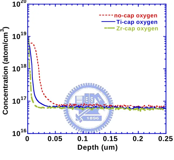
(50) 20. no-cap oxygen Ti-cap oxygen Zr-cap oxygen. 3. Concentration (atom/cm ). 10. 10. 19. 10. 18. 10. 17. 10. 16. 0. 0.05. 0.1 0.15 Depth (um). 0.2. 0.25. (c) Fig. 3.2c. (c) Oxygen contamination in nickel silicide in different capping conditions. This contamination can be eliminated by a novel Zr-cap layer.. 29.
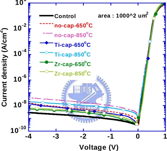
(51) 10. 0 2. area : 1000^2 um. 2. Current density (A/cm ). Control. 10. -2. o. no-cap-650 C o. no-cap-850 C o. Ti-cap-650 C. 10. -4. o. Ti-cap-850 C o. Zr-cap-650 C o. 10. -6. 10. -8. 10. Zr-cap-850 C. -10. -4. -3. -2. -1. 0. 1. Voltage (V). Fig. 3.3. Reverse current-voltage characteristics of all groups at silicidation temperature of 650ºC and 850ºC. The size of the junction area is 1000×1000 µm2.. 30.
(52) 3 2.5 2. Ln(-Ln(1-p)). 1.5 1 0.5 0 -0.5 -1 -1.5. Ni Ni Ni Ni. -2 -2.5 -3 -9 10. 10. -8. 10. 550 650 750 850. -7. 10. -6. 2. C urrent dens ity (A/cm ). (a) Fig. 3.4a. Weibull plots of leakage current density measured at -3V for non-capped Ni samples at different RTA conditions.. 31.
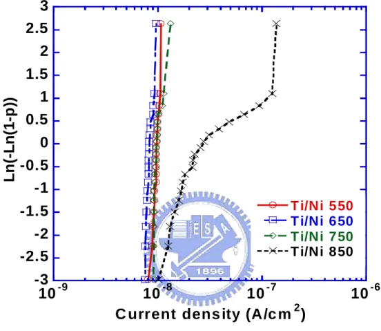
(53) 3 2.5 2. Ln(-Ln(1-p)). 1.5 1 0.5 0 -0.5 -1 T i/Ni T i/Ni T i/Ni T i/Ni. -1.5 -2 -2.5 -3 -9 10. -8. -7. 10 10 2 C urrent dens ity (A/c m ). 550 650 750 850. 10. -6. (b) Fig. 3.4a. Weibull plots of leakage current density measured at -3V for Ti capped. Ni samples at different RTA conditions.. 32.
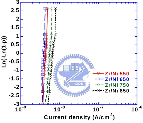
(54) 3 2.5 2. Ln(-Ln(1-p)). 1.5 1 0.5 0 -0.5 -1. Zr/Ni Zr/Ni Zr/Ni Zr/Ni. -1.5 -2 -2.5 -3 -9 10. -8. -7. 10 10 2 C urrent dens ity (A/c m ). 550 650 750 850. 10. -6. (c) Fig. 3.4c. Weibull plots of leakage current density measured at -3V for Zr capped. Ni samples at different RTA conditions.. 33.
(55) 3. Ln(-Ln(1-p)). 2.5 2 1.5 1 0.5 0 -0.5 -1. o. no-cap 650 C o Ti-cap 650 C o Zr-cap 650 C. -1.5 -2 -2.5 -3 0. 1. 2 3 4 5 6 7 8 9 -8 2 Current density (x10 A/cm ). 10. (a) Fig. 3.5a. Weibull plots of leakage current density measured at -3V for all silicided samples. (a) at RTA condition of 650ºC.. 34.
(56) 3. Ln(-Ln(1-p)). 2.5 2 1.5 1 0.5 0 -0.5 -1 o. -1.5 -2. no-cap 850 C. -2.5. Zr-cap 850 C. -3. o. Ti-cap 850 C o. 0. 5. 10. Current density (x10. 15 -8. 20 2. A/cm ). (b) Fig. 3.5b. Weibull plots of leakage current density measured at -3V for all silicided samples. (b) at RTA condition of 850ºC.. 35.
(57) Ni Ni Ni Ni. 60. o. 550 C o 650 C o 750 C o 850 C. y = 1.4764e-10 + 2.6121e-10x y = 8.6124e-11 + 2.0288e-10x y = 1.0914e-09 + 2.8481e-10x y = 1.4326e-09 + 6.3624e-10x. 50. -8. 2. Current density (x10 A/cm ). 70. 40 30 20 10 0. 0. 200. 400. 600. 800. 1000. -1. P/A ratio (cm ). (a) Fig. 3.6a. Comparison of the reverse junction leakage current density vs. the periphery to area ratio (P/A ratio) for (a) nickel silicide.. 36.
(58) 30 26 22. y y y y. = = = =. 1.5865e-10 7.8576e-11 3.3612e-10 5.8947e-10. + + + +. 2.1475e-10x 1.9060e-10x 1.9988e-10x 2.2346e-10x. -8. 2. Current density (x10 A/cm ). o. Ti/Ni 550 C o Ti/Ni 650 C o Ti/Ni 750 C o Ti/Ni 850 C. 18 14 10 6 2 0. 200. 400 600 800 -1 P/A ratio (cm ). 1000. (b) Fig. 3.6b. Comparison of the reverse junction leakage current density vs. the periphery to area ratio (P/A ratio) for (b) Ti-capped nickel silicide.. 37.
(59) -8. o. y = 4.7524e-11 + 9.8973e-11x y = 3.2173e-11 + 8.2277e-11x. o. y = 4.3673e-11 + 1.1158e-10x y = 4.7056e-11 + 1.3142e-10x. 18. Zr/Ni 550 C o Zr/Ni 650 C. 16. Zr/Ni 750 C. 2. Current density (x10 A/cm ). 20. o. Zr/Ni 850 C. 14 12 10 8 6 4 2 0 0. 200. 400 600 800 -1 P/A ratio (cm ). 1000. (c) Fig. 3.6c. Comparison of the reverse junction leakage current density vs. the periphery to area ratio (P/A ratio) for (c) Zr-capped nickel silicide.. 38.
(60) 10. -8. 2. Jra (A/cm ). Jra : Ni Jra : Ti-cap Ni Jra : Zr-cap Ni. 10. -9. 10. -10. 10. -11. 550. 650 750 o RTA Temp ( C). 850. (a) Fig. 3.7a. (a) Reverse junction area leakage versus the RTA temperature for all nickdel silicided junctions in different capping conditions.. 39.
(61) 10. -8. Jrp (A/cm). Jrp : Ni Jrp : Ti-cap Ni Jrp : Zr-cap Ni. 10. -9. 10. -10. 10. -11. 550. 650. 750. 850. o. RTA Temp ( C). (b) Fig. 3.7b. (b) Reverse junction periphery leakage versus the RTA temperature for all nickdel silicided junctions in different capping conditions.. 40.
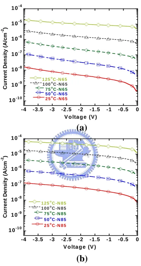
(62) -4. 10. -5. 10. -6. 10. -7. 10. -8. 10. -9. -2. Current Density (A/cm ). 10. o. 10. -1 0. -4. 1 25 C -N 6 5 o 1 00 C -N 6 5 o 7 5 C -N 6 5 o 5 0 C -N 6 5 o 2 5 C -N 6 5. -3.5. -3. -2.5 -2 -1.5 V o ltag e (V ). -1. -0.5. 0. -1. -0.5. 0. 10 10. -5. 10. -6. 10. -7. 10. -8. 10. -9. -2. Current Density (A/cm ). (a) -4. 10. o. -10. -4. 1 25 C -N 8 5 o 1 00 C -N 8 5 o 7 5 C -N 8 5 o 5 0 C -N 8 5 o 2 5 C -N 8 5. -3.5. -3. -2.5 -2 -1.5 V o ltag e (V ). (b) Fig. 3.8. Reverse currrent voltage characteristics of non-capped Ni samples measured at various temperatures. (a) samples with RTA 650oC (b) samples with RTA 850oC. 41.
(63) -2. Current Density (A/cm ). 10. -4. 10. -5. 10. -6. 10. -7. 10. -8. 10. -9. o. 10. 1 25 C -T 65 o 1 00 C -T 65 o 7 5 C -T 65 o 5 0 C -T 65 o 2 5 C -T 65. -1 0. -4. -3.5. -3. -2.5 -2 -1.5 V o ltag e (V ). -1. -0.5. 0. -1. -0.5. 0. 10. -4. 10. -5. 10. -6. 10. -7. 10. -8. -2. Current Density (A/cm ). (a). o. 10 10. 1 25 C -T 85 o 1 00 C -T 85 o 7 5 C -T 85 o 5 0 C -T 85 o 2 5 C -T 85. -9. -1 0. -4. -3.5. -3. -2.5. -2. -1.5. V o ltag e (V ). (b) Fig. 3.9. Reverse currrent voltage characteristics of Ti capped Ni samples measured at various temperatures. (a) samples with RTA 650oC (b) samples with RTA 850oC. 42.
(64) -4. 10. -5. 10. -6. 10. -7. 10. -8. 10. -9. -2. Current Density (A/cm ). 10. o. 10. 1 25 C -Z r65 o 1 00 C -Z r65 o 7 5 C -Z r65 o 5 0 C -Z r65 o 2 5 C -Z r65. -10. -4. -3.5. -3. -2.5 -2 -1.5 V o ltag e (V ). -1. -0.5. 0. -1. -0.5. 0. Current Density (A/cm-2). (a) 10. -4. 10. -5. 10. -6. 10. -7. 10. -8. 10. -9. o. 10. 1 25 C -Z r85 o 1 00 C -Z r85 o 7 5 C -Z r85 o 5 0 C -Z r85 o 2 5 C -Z r85. -10. -4. -3.5. -3. -2.5 -2 -1.5 V o ltag e (V ). (b) Fig. 3.10. Reverse currrent voltage characteristics of Zr capped Ni samples measured at various temperatures. (a) samples with RTA 650oC (b) samples with RTA 850oC. 43.
(65) -32 Ni850 : Ea=0.90eV. Ln(IR/T3). -34. -36. -38. Ni650 : Ea=1.06eV. -40. -42 1.8. 1.9. 2. 2.1. 2.2. 2.3. 2.4. 2.5. 1/kT (X1020). (a) Fig. 3.11a. Arrhenius plot (Ln IR/T3 versus 1/kT) for non-capped nickel silicide schottky junction after RTA at 650oC and 850oC, respectively measured at -3V.. 44.
(66) -33 Ti850 : Ea=0.95eV. -34. -36. 3. Ln(IR/T ). -35. -37 -38 -39 -40 -41 1.8. Ti650 : Ea=1.06eV. 1.9. 2. 2.1. 2.2. 2.3. 2.4. 2.5. 1/kT (X1020). (b) Fig. 3.11b. Arrhenius plot (Ln IR/T3 versus 1/kT) for Ti capped nickel silicide schottky junction after RTA at 650oC and 850oC, respectively measured at -3V.. 45.
(67) -32 Zr850 : Ea=1.08eV. 3. Ln(IR/T ). -34. -36. -38. -40 Zr650 : Ea=1.08eV. -42 1.8. 1.9. 2. 2.1. 2.2. 2.3. 2.4. 2.5. 1/kT (X1020). (c) Fig. 3.11c. Arrhenius plot (Ln IR/T3 versus 1/kT) for Zr capped nickel silicide schottky junction after RTA at 650oC and 850oC, respectively measured at -3V.. 46.
(68) Chapter 4 Ultra-Shallow Junction Formation by PH3 Plasma Immersion Method 4.1 Introduction. For complementary metal-oxide-semiconductor (CMOS) technology to meet the demanding scaling requirements, ultra shallow and low resistance junctions are required to suppress short channel effect (SCE) and to obtain high current drivability [1]. For the formation of ultra-shallow junction, the transient enhanced diffusion (TED) effect and channeling effect are the major problems. Numerous solutions have been proposed such as solid phase diffusion (SPD), pre-amorphizing ion implantation (PAI), low energy ion implantation (LII), plasma doping (PD) and laser annealing (LA) [2-8]. For SPD method, It has the advantage of not demonstrating transient enhanced diffusion effects. However, it is very difficult to control the thickness of screen oxide and the ion implantation energy which can remain the implanted dopants and the damages within screen oxide. In the view of PAI way, it is a good way to form a shallow junction by the channeling effect suppression. Nevertheless, the major problem for Si pre-amorphizing ion implantation is much more defects induce larger leakage ~ 10-8A/cm-2 and a large spread of leakage current. New annealing processes should be developed to minimize density of defects. Table 4.1 shows the trend of source and drain extension junction depth and sheet resistance in 1999 ITRS [9]. To 47.
(69) meet these needs, surface reaction doping was first introduced [9]. By this method, the defects result from ion implantation can be avoided. However, the plasma damage will be produced in the meantime. In this chapter, we compared LA and PD method for ultra shallow junction formation and focus our investigation on the plasma doping without vertical bias method to eliminate the defects result from doping process.. 4.2 Experimental. Fig. 4.1 shows the process flow and schematics for the fabrication of n+/p junction by PH3 plasma immersion. Following a standard Radio Corporation of America (RCA) cleaning process, a 500nm-thick field oxide was thermally grown on the p-type (100) oriented Si wafer with 3-5 Ω-cm at 1050°C for one hour. After isolation oxide formation, the active regions were defined by photolithography and etched by BOE (Buffer oxide etcher) solution. Subsequently, RCA clean was performed for eliminating the contamination. Then, the PH3 plasma immersion was used to form an n+/p junction with RF power 50W for 1, 5, and 10minutes, respectively. Parts of samples were capped with oxide layers before dopant activation. After plasma immersion, rapid thermal annealing (RTA) was carried out to formed n+/p junctions at 850℃, 900℃, 950℃, and 1000℃ for 10sec and 30sec, respectively, in nitrogen ambient. At final. 48.
(70) metallization process, a thin TiN of about 25nm was deposited as a barrier layer and aluminum was deposited immedately for both the front and backside electrode. Table 4.2 is the split table of different annealing conditions for ultra shallow junction formation by PH3 plasma immersion.. 4.3 Results and Discussion. 4.3.1 Sheet Resistance and SIMS Analysis of PH3-Plasma Immersion Junction. Sheet resistances of all samples were examined with a four-point probe. Fig. 4.2a, shows the sheet resistance of PH3 plasma immersion junction activated by excimer laser with different energy. Fig. 4.2b exhibits the sheet resistance of the junction annealed by different laser energy and then with RTA 950oC for 30s. In Fig. 4.2c, the sheet resistance versus different laser energy of plasma doped junction with cap-oxide is extracted. It seems that dopant at the surface can't be activated even the laser energy up to 300mJ/cm2. Fig 4.3 is the plot of sheet resistance vs. different RTA conditions of plasma doped junction with and without cap-oxide by 50W RF power for 5 minutes. And Fig. 4.4a, b and c show the sheet resistance of n+/p junction doped by PH3 plasma with 50W RF power for 1, 5 and 10 minutes, respectively. The sheet resistance of the junction with a oxide cap is much lower than that without capping. And the higher activation temperature is used, the lower sheet resistance is 49.
數據
+7

Outline
相關文件
FPGA –現場可規劃邏輯陣列 (field- programmable
FPGA –現場可規劃邏輯陣列 (field- programmable
FPGA –現場可規劃邏輯陣列 (field- programmable
The prepared nanostructured titania were applied for the photoanodes of dye-sensitized solar cell.. The photoanodes were prepared by the doctor blade technique and the area
➢ Plot the learning curves (ROUGE versus training steps)... ➢ What is your final
GaN transistors with high-power, High temperature, high breakdown voltage and high current density on different substrate can further develop high efficiency,
Several methods that modulation effective work function to maintain p-type gate material is the direction of future research, sush as microwave annealing with plasma
FPGA(Field Programmable Gate Array)為「場式可程式閘陣列」的簡稱,是一 個可供使用者程式化編輯邏輯閘元件的半導體晶片
