國立交通大學
材料科學與工程學系
博士論文
一維氧化鋅的合成與結構對於光電特性
及生醫應用的研究
Study on Synthesis and Structure of One
Dimensional Zinc Oxide for
Optoelectronic Characteristics and
Bio-Medical Applications
研究生 : 蕭繼聖
指導教授 : 陳三元 博士
Contents
Contents I 摘要 IV Abstract V 誌謝 VII Chapter 1 ………...1Chapter 2 Literature Review... 4
2.1 ZnO nanorods ... 4
2.1.1 Introduction ... 4
2.1.2 Crystal and surface structure of ZnO ... 5
2.1.3 Growth ZnO nanorods ... 5
2.1.4 ZnO defect chemistry ... 6
2.1.5 Applications of the ZnO nanorods ... 8
2.2 ZnO nanotubes... 9
2.3 Nano-Alumina material ... 11
2.3.1 Structure and phase of alumina material... 11
2.3.2 Synthesis and optical of nano-alumina material... 12
2.4 ZnO Core/shell materials... 13
2.5 ZnO nanostructure in the bio-medical application ... 14
Chapter 3Experimental materials and methods... 26
3.1 Flow chart of experimental procedure ... 26
3.2 ZnO thin films formation... 27
3.3 Wet-chemical growth of ZnO nanorods and nanotubes ... 27
3.4 Wet-chemical synthesis of alumina nanoparticles and nanofilms ... 27
3.6 Characterization of ZnO and alumina materials ... 29
Chapter 4Tunable growth of ZnO nanorods synthesized in aqueous solutions at low temperatures... 30
4.1 Introduction ... 30
4.2 ZnO nanorods with different growth parameters ... 31
4.3 Patterned growth of the ZnO nanorods... 32
4.4 The relation between ZnO film and ZnO nanorods ... 33
4.5 Summary ... 34
Chapter 5Growth behavior and microstructure evolution of ZnO nanorods grown on Si in aqueous solution... 44
5.1 Introduction ... 44
5.2 Phase and morphology of ZnO nanorods grown on different substrates ... 45
5.3 Microstructural analysis of ZnO nanorods... 46
5.4 Growth behavior of ZnO nanorods ... 48
5.5 Summary ... 50
Chapter 6Synthesis and Luminescent Properties of Strong Blue Light-Emitting Al2O3/ZnO Nanocables ... 59
6.1 Introduction ... 59
6.2 The structure of the Al2O3/ZnO nanocables ... 60
6.3 Annealing effect on the Al2O3/ZnO nanocables ... 62
6.4 The investigation of photoluminescence centers in the Al2O3/ZnO nanocables . 63 6.5 Summary ... 67
Chapter 7Synthesis and Optical Properties of White-light Emitting Alumina/ZnO Nanotubes ... 76
7.1 Introduction ... 76
7.3 The structure of the ZnO nanotubes after thermal annealing ... 79
7.4 The structure of the alumina/ZnO nanotubes ... 81
7.5 The optical properties of the alumina/ZnO nanotubes ... 82
7.6 Summary ... 84
Chapter 8Smart ZnO nanotube for Controlled Drug Release ... 96
Chapter 9Conclusions ... 109
References... 111
Curriculm Vitae ... 116
摘要
氧化鋅被視為明星的奈米材料之一,由於其寬廣的能隙(3.37 eV),並且具有卓越 的化學和熱穩定性,使得在眾多產業上有著很好地應用。隨著一維奈米材料的發展,如 何合成一維氣化鋅奈米結構,就變成了一項重要的研究。在過去幾年,發展出利用低溫 溶液法成長氧化鋅奈米結構,並且,可以控制成長好幾種的形態。然而,氧化鋅本身的 複雜地缺陷結構,卻大大地影響了其應用。因此,如何改善和操控缺陷,就變成了一項 非常值得深入的研究主題,另外,一個聰明的氧化鋅元件,在生物醫學方面的研究,也 是令人期待。所以,本論文研究會深入地探討,一維氧化鋅的合成即其光學特性、氧化 鋁-氧化鋅殼核結構的光學性質,最後會利用染料摸擬藥物釋放,來研究藥物載體(氧化 鋅)在電場下的釋放行為。 在第一章,我們會一般地介紹氧化鋅材料。在第二章,將會討論氧化鋅的基本特性、 缺陷、製程、應用和生醫藥物。第三章將會介紹實驗製程,包含氧化鋅和氧化鋁-氧化 鋅殼核結構的製程,並且,量測方法和設備皆會在這章做介紹。 第四章主要會說明氧化鋅奈米柱如何經由水溶液法成長在,鍍有氧化鋅薄膜的矽基 版上,而其成長的形態跟薄膜上的晶粒大小有絕對的關係。第五章將會討論在兩種基版 上氧化鋅奈米柱的成長行為。 第六章將會展示陣列式氧化鋁-氧化鋅殼核奈米結構,經由溶凝膠法在室溫所製 成,並且經由光譜分析得知,此結構在 400o C、600o C 的氧氣、氮氣熱處理後,能發出在 450 nm 強烈藍光。第七章將會先介紹如何經由化學溶液法,合成氧化鋅奈米管,更進一 步展示氧化鋁-氧化鋅奈米管的成長。在經過不同溫度和氣氛熱處理下,此奈米管將會 發出各種不同顏色的光,經由高斯分析可知,這些光有藍、藍-綠,綠和黃光,這些光 和奈米管的缺陷有強烈的相關性。 最後,在第八章將會展示如何用高頻電場控制 FITC-ZnO 奈米管的釋放行為。另外, 也可以證明此氧化鋅結構,具有低能量損耗、良好的生物相容性、生物標示和低成本的 特性。Abstract
ZnO has been recognized as one of the promising nanomaterials in a broad range of high-technology applications because ZnO has a large direct band gap (3.37 eV), excellent chemical and thermal stability, and the electrical properties of a large exciton binding energy (60 meV). Furthermore, with one-dimensional materials developing, the synthesis of one-dimensional ZnO nanostructure becomes an important research. In the past several years, a low-temperature solution-based method to prepare complex ZnO nanostrucutes has been developed. In addition, ZnO morphology can be controlled via simple solution route. However, a fatal problem for ZnO material is complex defects. Therefore, it is worth to be studied on how to improve and manipulate defects. In addition, ZnO nanostructures are believed to be nontoxic and possibly biocompatible. A smart ZnO device for bio-medical is expected to develop. Therefore, this thesis outlines the process and optical of one-dimensional ZnO nanstructures and the study of photoluminescent properties and light-emitting characteristics of ZnO/alumina core/shell nanostructure. Finally, Drug release behavior from dye-ZnO nanostructure by applying high frequency electric field is also given in this thesis.
In chapter 1, we will present an introductory overview to ZnO materials. Chapter 2 will discuss fundamental, defects, synthesis process, application and bio-medical. Chapter 3 will introduce the experimental process, including ZnO and alumina-coated ZnO nanostructure. The measurement setup for optoelectronic characteristics is also shown in this chapter.
Chapter 4 will demonstrate that highly arrayed ZnO nanorods were fabricated on the Si substrate buffered with patterned ZnO film (ZnOf/Si) via wet-chemical process. It was found that the growth morphology of ZnO nanorods is strongly dominated by the grain size of the ZnO film on the Si substrate. Chapter 5 will discussed growth behavior of the ZnO nanorods. Two substrates, Si and ZnO film-coated Si (ZnOf/Si), were used to investigate growth
behavior and microstructure evolution of single-crystal ZnO nanorods (ZNs) in aqueous solutions at low temperatures.
Chapter 6 will show that hetrostructured AlOx-ZnO core-shell nanocables arrays have been successfully synthesized by soaking the ZnO nanorods in the sol-gel solution of Al(NO3)3 and NH4OH at room temperature. Photoluminescence measurement indicates that a strong blue emission peak at ~450 nm appears at 400oC and 600oC in O2 and N2 atmospheres, respectively. Chapter 7 will induce to synthesize the ZnO nanotubes by chemical solution method. Moreover, a simple chemical solution process for alumina/ZnO nanotubes will be studied. After thermal treatment at different temperatures under various atmospheres, photoluminescence (PL) measurements showed that the alumina nanoparticles coated on ZnO nanotubes (ANZTs) emitted a variety of colors, including blue, green and white light. Gaussian curve fitting of the PL spectra revealed that the competition between the blue, blue-green, green and yellow band emissions and their relative emission intensities were strongly associated with various defects.
Finally, Chapter 8 will demonstrate the controlled release behavior of the FITC-ZnO nanotubes by high frequency electric-field. This ZnO-based nanostructure possesses low power consumption, biocompatible, bio-imaging and low-cost characteristic.
誌 謝
在這漫長的求學路途上,我首先想感謝我的父母,沒有他們的幫助,我不可能可以 完成我的學業,他們的默默支持,是我可以全力專心研究的最大助力。接下來,我想感 謝我的指導教授-陳三元,把我從一位不會做學術研究的學生,在他的不放棄的指導下, 學生終於對於如何做研究,有了些許的心得。另外,我也很感謝另一位教授-劉典謨, 對我研究路途上的幫助,他教會我如何深入做研究。再來,我想感謝可愛的琬琳學妹, 在她的幫助下,我完成了很多複雜的實驗,沒有她,我想我不可能可以完成這論文的深 度。接下來,我想感謝晉慶學長,有他的幫助,幫我解答了很多深入的問題,以及他對 我細心的照顧。另外,我想感謝尚秀和維琳,在他們兩位的幫助下,我才能完成我論文 的最後一部份,以及帶我認識不熟悉的領域。除此之外,我要感謝實驗室的每一位同學 和學弟妹,因為,有他們才能使我有愉快的博士生活,抱持快樂的心態。Chapter 1
Introduction
Low-dimensional nanostructural materials have been extensively studied for their application in photonic and electronic devices, for example, GaN, ZnO and ZnS. They have attracted considerable interest in application to ultraviolet (UV) laser devices due to their direct wide band gaps. Among them, ZnO (△Eg = 3.37) is thought to be the most suitable material for UV laser devices due to its large excition binding energy of 60 meV compared to the thermal energy (26 meV) of room temperature.[1-4] ZnO is belonging to wurtzite structure which are the noncentral symmetry and polar surfaces. The structure of ZnO can be assigned to a number of alternating planes composed of tetrahedrally coordinated O-2 and Zn+2 ions, stacked along the c-axis. Therefore, the ZnO is a good candidate for applications in optoelectronices, lasing, and piezoelectricity. Recently, arrays of ZnO nanorods are expected to speed charge migration for solar cell application, due to their lower trap density and more direct path to the current collecting electrode. In order to increase surface volume ratio for raising sensitivity, ZnO nanotubes are good candidate material.[5] Furthermore, ZnO is also a bio-safe and biocompatible, which can be used for biomedical application without coating.[6]
Nowadays, various synthetic approaches have been developed to fabricate ZnO nanostructures, which can be classified into two categories, vapor-phase and solution-phase synthesis. Vapor-phase processes such as vapor-liquid-solid growth (VLS),[7] chemical vapor deposition (CVD),[8] thermal decomposition,[9] and thermal evaporation[10] are favored for their simplicity and high-quality products. Solution-phase routes are appealing due to their low growth temperature, low cost, high efficiency, and potential for scale up. On the other
side, many morphology of ZnO nanostructure have been discovered by various synthesized processes, such as nanobelts, nanosprings, nanorings, nanorods, nanotubes.[12-15]
Although one dimension ZnO nanorods and nanotubes show very attractive properties, such as electric, optical and bio-safe properties, it is an important issue how to tune the ZnO nanorods growth by wet-chemical method. Therefore, in the PhD thesis, several main topics will be investigated. (i) In Chapter 4, we will first study the synthesis and growth control of highly arrayed ZnO nanorods on the Si substrate buffered with patterned ZnO film (ZnOf/Si) via wet-chemical process. The growth behavior and morphology of single-crystal ZnO nanorods (ZNs) were investigated in terms of the annealing temperatures of the sputtered ZnO film.(ii) In Chapter 5, the growth behavior of ZnO nanorods will be focused. Two substrates, Si and ZnO film-coated Si (ZnOf/Si), were used to investigate growth behavior and microstructure evolution of single-crystal ZnO nanorods (ZNs) in aqueous solutions at low temperatures. (iii) ZnO nanorods have been used for LED application for many years and ZnO nanorods can be used are good template due to good conduct electricity. Therefore, in Chapter 6, the photoluminescence and and HRTEM interface microstructure of the AlOx-ZnO core-shell nanocables will be investigated and discussed. (iv) Recently, ZnO nanotubes have attracted more attention due to excellent properties, such as high surface/volume ratio. Therefore, in Chapter 7, we will first invstigate the synthesis of the ZnO nanotubes by chemical solution method. Next, in order to develop white light LED, a simple chemical solution process developed for alumina/ZnO nanotubes will be studied. The photoluminescence (PL) measurements of the alumina/ZnO nanotubes after thermal treatment at different temperatures under various atmospheres will be further analyzed. (v) Since ZnO materials have been believed to be nontoxic, biosafe, and possibly biocompatible, it could be developed for biomedical applications in our daily life, such as drug carriers and cosmetics. Therefore, in Chapter 8, we will introduce the ZnO nanotubes in the application of drug carriers. It was demonstrated that drug released from the ZnO nanotubes can be controlled by
the ZnO-based electric device. Furthermore, a test with the cell will be performed on the bio-imaged ZnO nanostructures. Finally, conclusions and future researches will be summarized.
Chapter 2
Literature Review
2.1 ZnO nanorods 2.1.1 Introduction
Nanostructured ZnO materials have attracted much attention due to their exceptional performance in electronics, optics and photonics. From the 1960s, synthesis of ZnO thin films has been an active field because of their applications as sensors, transducers and catalysts. In the last few decades, especially since the nanotechnology initiative led by the US, study of one-dimensional (1D) materials has become a leading edge in nanoscience and nanotechnology. With decreasing volume size, novel electrical, mechanical, chemical and optical properties are introduced, which are believed to be the result of surface and quantum confinement effects. Nanowire-like structures are the ideal system for studying the transport process in one-dimensionally (1D) confined objects, which are of benefit not only for understanding the fundamental phenomena in low dimensional systems, but also for developing new generation nano-devices. ZnO is a key technological material. The lack of a centre of symmetry in wurtzite, combined with large electromechanical coupling, results in strong piezoelectric and pyroelectric properties and the consequent use of ZnO in mechanical actuators and piezoelectric sensors. In addition, ZnO is a wide band-gap (3.37 eV) compound semiconductor that is suitable for short wavelength optoelectronic applications. The high exciton binding energy (60meV) in ZnO crystal can ensure efficient excitonic emission at room temperature and room temperature ultraviolet (UV) luminescence has been reported in disordered nanoparticles and thin films. ZnO is transparent to visible light and can be made
highly conductive by doping. ZnO is a versatile functional material that has a diverse group of growth morphologies, such as nanocombs, nanorings, nanosprings, nanobelts, nanowires and nanocages. The basic materials parameters of ZnO are shown in Figure 2.1.
2.1.2 Crystal and surface structure of ZnO
Wurtzite zinc oxide has a hexagonal structure (space group C6mc) with lattice parameters a = 0.3296 and c = 0.52065 nm. The structure of ZnO can be simply described as a number of alternating planes composed of tetrahedrally coordinated O2− and Zn2+ ions, stacked alternately along the c-axis (Figure 2.2[16]). The tetrahedral coordination in ZnO results in non central symmetric structure and consequently piezoelectricity and pyroelectricity. Another important characteristic of ZnO is polar surfaces. The most common polar surface is the basal plane. The oppositely charged ions produce positively charged Zn-(0001) and negatively charged O-(0001) surfaces, resulting in a normal dipole moment and spontaneous polarization along the c-axis. To maintain a stable structure, the polar surfaces generally have facets or exhibit massive surface reconstructions, but ZnO ± (0001) are exceptions: they are atomically flat, stable and without reconstruction.[17,18] The other two most commonly observed facets for ZnO are {2110} and {0110}, which are non-polar surfaces and have lower energy than the {0001} facets.
2.1.3 Growth ZnO nanorods
The different surface structures of ZnO could induce anisotropic growth. Under thermodynamic equilibrium conditions, the facet with higher surface energy is usually small in area, while the lower energy facets are larger. Specifically, in the ZnO growth, the highest growth rate is along the c-axis and the large facets are usually {0110} and {2110}. Therefore, the ZnO nanorods can be synthesized by many process, including chemical bath deposition(CBD)[19,20], aqueous chemical solution[21], and vapour-liquid-solid (VLS)[22].
The growth mechanism from VLS method was proposed in the 1960s-1970s for large whisker growth. This method is promotion of anisotropic crystal growth using metal nanoparticles as catalysts. Yang et al. [22] reported the use of the vapor-phase transport process to grow ZnO nanowires via the VLS mechanism. The Zn vapor was generated using carbothermal or hydrogen reduction of ZnO. Size control of the nanowire diameters was achieved by varying the thickness of the thin film Au catalyst.
Another important growth method is aqueous chemical method. Vayssieres et al. [21] used this method to grow nanorods on conducting glass and Si substrates. For this type of growth, a ZnO seed layer is needed to initialize the uniform growth of oriented nanorods. Often, a solution of Zn(NO3)2 and hexamethyltetramine (HMT) is used:
(CH2)6N4 + 6H2O ↔ 6HCHO + 4NH3 (1)
NH3 + H2O ↔ NH4+ + OH- (2)
2OH- + Zn2+ → ZnO(s) + H2O (3)
Hydroxide ions are formed by the decomposition of HMT and they react with the Zn2+ to form ZnO.
Idealized growth habit of a ZnO crystal was first to describe by Laudise [23,24] by the hydrothermal method. It has been observed that the maximal crystal growth velocity is fixed in the <0001> direction and the following relationship between the velocities of crystal growth to different directions is found to be: V<0001>
>
V<0110>>
V<0001>. Because the fastest growth plane (0002) will be disappeared, the shape of ZnO nanostructure would become wires or rods.2.1.4 ZnO defect chemistry
There are a number of intrinsic defects with different ionization energies in ZnO structure. The Kroger Vink notation uses: i = interstitial site, Zn = zinc, O = oxygen, and V = vacancy. The terms indicate the atomic sites, and superscripted terms indicate charges, where a dot
indicates positive charge, a prime indicates negative charge, and a cross indicates zero charge, with the charges in proportion to the number of symbols. Figure 2.3 shows that there are a number of defect states within the bandgap of ZnO. The donor defects are: •• i Zn , • i Zn , x i Zn , •• o V , • o
V ,Vo and the acceptor defects are:V ′′Zn,V ′Zn. The defect ionization energies vary from ~0.05-2.8 eV. Zn interstitials and oxygen vacancies are known to be the predominant ionic defect types.[25]
Figure 2.4 [26]shows the corrected formation energies for the relevant native point defects in ZnO as a function of Fermi-level position. The kinks in the curves for a given defect indicate transitions between different charge states. The differences are related to the correction of absolute formation energies, where we now take into account the occupancy of the defect-induced states in the case of defects with partially occupied states in the band gap. Oxygen vacancies have the lowest formation energy (see Fig. 2.4). Oxygen vacancies have frequently been invoked as the source of unintentional n-type conductivity in ZnO. Prof. Vanheusden found that the green emission intensity is strongly influenced by free-carrier depletion at the particle surface, particularly for small particles and/or low doping. Their data suggested that the singly ionized oxygen vacancy is responsible for the green emission in ZnO; this emission results from the recombination of a photogenerated hole with the singly ionized charge state of this defect. [26]
Because of the different ionization energies, the relative concentrations of the various defects depend strongly on temperature. However, the partial pressure of oxygen and zinc,
pO2 and pZn, respectively, are also very important. Hence, under very reducing conditions
and at high temperatures, oxygen vacancies may predominate, depending on the relative
pO2/pZn ratio. During annealing, the variety of these defects with the oxygen pressure (PO2)
Equations (4) and (6) indicate that concentrations of the oxygen vacancy and the interstitial zinc decreased with the increase of oxygen pressure
2
O
P : While Eqs. (5), (7) and (8) indicated
that concentrations of the zinc vacancy, the interstitial zinc and antisite oxygen increased with the increase of the oxygen pressurePO2. [27]
2.1.5 Applications of the ZnO nanorods
So far, there are many applications of the ZnO nanorods, such as sensor, light-emitting diodes, lasing, cantilevers and solar cells. Especially, solar cells and lasing are the two famous applications. Prof. Yang reported nanowire dye-sensitized solar cells in 2005. They introduced a version of the dye-sensitized cell in which the traditional nanoparticle film wass replaced by a dense array of oriented, crystalline ZnO nanowires. The nanowire anode wass synthesized by mild aqueous chemistry and features a surface area up to one-fifth as large as a nanoparticle cell. The direct electrical pathways provided by the nanowires ensured the rapid collection of carriers generated throughout the device, and a full Sun efficiency of 1.5% was demonstrated. The device structure is presented in Figure 2.5. [28]
Laser application of the ZnO nanorods is also quite attracted much attention up to now. Prof. Choy show the room-temperature ZnO ultraviolet laser in 2003. They presented that a high-quality ZnO nanrods was grown on a Si wafer by a wet-chemical process at 95oC, where the Si wafer was dip-coated with 4 nm sized ZnO nanoparticles s buffer and seed layer prior
(4) (5) (6) (7) (8)
th the crystal growth. The product ZnO nanrods showed threshold power density was ~70kW cm-2. The result can be seen in the Figure. 2.6. [29] Moreover, Prof. Wang developed a direct-current nanogenerator driven by ultrasonic waves in 2007. The nanogenerator was fabricated with vertically aligned zinc oxide nanowire arrays that were placed beneath a zigzag metal electrode with a small gap. The wave drives the electrode up and down to bend and/or vibrate the nanowires. A piezoelectric semiconducting coupling process converts mechanical energy into electricity. The zigzag electrode acts as an array of parallel integrated metal tips that simultaneously and continuously create, collect, and output electricity from all of the nanowires. The approach presents an adaptable, mobile, and cost-effective technology for harvesting energy from the environment, and it offers a potential solution for powering nanodevices and nanosystems. The nanogenerator structure was shown in the Figure 2.7. [30]
2.2 ZnO nanotubes
It is well-kwon that the hollow structure provides 1D ZnO with more prominent advantages than other 1D ZnO materials. For example, the formation of tubes facilitates enhancing the confinement effect in 1D structures and tuning the electronic properties of materials in a wider range. Moreover, a larger surface area-volume ratio in tubular structure provides an effective way to optimize the performances of various devices including dye-sensitized photovoltaic cells, catalysts, gas sensors, and hydrogen storage. But, few publications on the preparation of ZnO nanotubes (NTs) have been reported because the tubular form is generally limited in layered materials such as carbon nanotube so that it seems hard to obtain the tubular structure for the nonlayered ZnO material. This situation was improved from chemical solution process produced. L. Vayssieres et al. reported a famous paper, three-dimensional array of highly oriented crystalline ZnO microtubes. They presented a simple chemical solution mehod. A equimolar (0.1 M) aqueous solution of zinc nitrate, Zn(NO3)2.4H2O, and
ITO-coated polyester substrate washed and cleaned with MilliQ water. The bottle is then heated at a constant temperature of 90°C for 2 days in a regular laboratory oven. Subsequently, the homogeneous thin films are thoroughly washed with water to remove any contamination from residual salts or amino complex. This concept was schemed in the figure 2.8. [31]
However, the growth mechanism of the ZnO NTs was not clear. After five years ago, Sun and co-workers supplied growth theory. They proposed that the different surface terminations influence (through electrostatic interactions) the cation (Zn2+) to anion (OH-) concentration ratio in the double layer at the growing polar surface. Zn-atom termination causes a reduction in the local Zn2+/OH- ratios (i.e. the extent of solution supersaturation) relative to those in the bulk solution, thereby encouraging tapered NR growth and, as the zinc concentration falls further, the emergence of volcano-like structures on the polar surface which seed the subsequent growth of ZnO NTs, as shown in Figure 9. [32]
However, Han et al. thought this chemical solution process remained complex and difficult/irreproducible. They reported the low-temperature synthesis of hexagonal ZnO nanotube arrays, which can be formed on zinc foils. This process could further reduce the growth temperature to 65oC.
Optical properties of the ZnO NTs are expected to study. Zhang reported strong green emission of ZnO NTs. It is well-known that ZnO has green light emission, which has been attributed to the singly ionized oxygen vacancy in ZnOand is located at ~2.2 and ~2.5 eV, as shown in Figure 2.10. [33] They pointed out that NTs have enhanced green emission due to a much improved surface area, which is predominant over the near-band edge emission. In other words, a higher surface area to volume ratio should favor a higher level of surface and subsurface oxygen vacancies.
ZnO nanowires solar cell did not demonstrate good enough efficiency, limited primarily by the surface area of the nanowire array. ZnO NTs can just overcome this problem. Hupp et al. introduced high surface area ZnO NT photoanodes templated by anodic aluminum oxide for
use in dye-sensitized solar cells. While the new nanotube cells compare favorably with other ZnO-based DSSCs, increased surface area will clearly be needed because of energy conversion efficiencies approaching that of the best ZnO cells (4%). [34]
2.3 Nano-Alumina material
2.3.1 Structure and phase of alumina material
Alumina is a low cost material used in many domains like catalysis, ceramics and mechanical ceramics, refractory, electrotechnology, electronics, bio-medical,. . .. The wide variety of these applications comes from the fact that alumina occurs in two forms, corundum or α-alumina with a hexagonal close-packing of oxygen ions and transition aluminas with a cubic close packing of oxygen. Transition aluminas include a series of metastable forms that exist on an extended temperature range, but all of them lead to α-alumina by calcining at high temperatures. Corundum has excellent mechanical, electrical, thermal, and optical properties. Transition aluminas are widely used as adsorbents, catalysts, catalyst supports, and membranes because of their high surface area, mesoporosity, and surface acidity.
Transition aluminas are prepared by calcining aluminum hydroxides. As different hydroxides were used, it usually leads to different forms having different thermal stability, surface acidity and textural properties. Among aluminum hydroxides, boehmite, aluminum oxyhydroxide (AlOOH) is an important precursor because the heat treatment of boehmite produces a series of transition aluminas from γ-Al2O3 and η- Al2O3 to δ-Al2O3, and θ-Al2O3, which exhibit high surface areas (200–500 m2/g) and thermal stability up to 1000oC. [35] The structures of the transition aluminas all are based on a face-centered cubic (fcc) array of oxygen anions. The structural differences between these forms only involve the arrangement of aluminum cations in the interstices of the fcc array of oxygen anions. γ-Al2O3 and η-Al2O3 have defect spinel structures. δ-Al2O3 has a tetragonal superstructure of the spinel lattice with
one unit-cell parameter tripledand θ-Al2O3 has a monoclinic structure. η-Al2O3 is produced by dehydration of bayerite Al(OH)3, whereas γ-Al2O3 is formed by dehydration of boehmite. Upon heating, γ-Al2O3 and η-Al2O3 are gradually converted in θ-Al2O3.
Boehmite was thought to exist under two distinct forms, well-crystallized boehmite and pseudoboehmite (also called gelatinous boehmite), with significantly different morphologies, porosity, and surface areas. [36] Pseudo-boehmite is a low crystalline aluminum oxide hydroxide. The crystal structure is consisted of a distorted AlO6 octahedron, which is joined by sharing edges to form zigzagged layers parallel to the (010) plane. These layers are linked together by hydrogen bonds between hydroxyls in neighboring layers. Although pseudo-boehmite contains water molecules between layers, the intercalation of guest molecules is very difficult because of strong hydrogen bonding between the layers. γ-alumina is reported to occur at temperatures between 350 and 1000 °C. It is typically formed from an amorphous or boehmite precursor and has remained present at temperatures as high as 1200 °C when derived from amorphous aluminas. The bulk structure of g alumina is closely related to that of magnesium spinel (MgO,Al2O3). [37]
2.3.2 Synthesis and optical of nano-alumina material
Alumina powders have been synthesized by Bayer process since 1888. Up to now, there are many methods to fabricate alumina powders, such as solid state deposition, precipitation, sol-gel and chemical vapor deposition. The main fabricated process in industry is Bayer process. On the other hand, sol-gel methods are a cheap and conventional process. Yoldas et al. [38] reported that transparent monolithic alumina could be obtained by the sol-gel method using an alumina sol derived from the alkoxide. Furthermore, Suga and co-workers [39] prepared transparent alumina gels from two sources, AlCl3·6H2O and aluminium iso-propoxide. The boehmite phase is synthesized first and usually the phase is amorphous.
Then, the thermal process can be used to promote the boehmite to transform α-alumina phase through γ-alumina.
Blue photoluminescent emission was observed in pure nanometer-sized γ-alumina powders prepared by the sol-gel process. The photoluminescent emission spectra were made up of a broad band and the emission band of 422 nm had obvious intensity. Du et al. used the alumina membrains with nano pore arrays to point out that the blue emission band is related to the singly ionized oxygen vacancies (F+ centers). However, the formation mechanism of F+ centers is not clear. Ishizaka and co-workers presented that the F+ centers may be related to pentahedrally (AlV) coordinated aluminum by NMR result. Boehmite phase is belong to octahedrally (AlVI) coordinated alumina. However, the γ-alumina has tetrahedrally and octahedrally coordinated alumina. They supposed that the pentahedrally coordinated aluminum would be produced during the phase transformation. [40,41]
2.4 ZnO Core/shell materials
The nanostructures of optical materials are particularly important as the properties of these materials are greatly influenced by various surface states arising out of the higher surface-to-volume ratio. This can be further tuned by deliberately modifying the surface of nanostructured materials by other materials such as core-shell nanostructures. ZnO core/shell structure was wild application in the fields of luminescence, electronics, and sensors. Chaudhuri et al. have successfully fabricated vertically aligned ZnO-ZnS core-shell and ZnS nanorods arrays in a thin film form by sulfidation of aligned ZnO nanorod arrays. [42] The PL study at room temperature indicated that the high band gap ZnS shell confines the photogenerated carriers inside the ZnO core, and so enhanced UV emission was observed for the ZnO-ZnS core-shell nanorods, when the shell thickness is a few nanometers. Yang et al. [43] described the construction and performance of dye-sensitized solar cells (DSCs) based on arrays of ZnO nanowires coated with thin shells of amorphous Al2O3 by ALD. The TEM
images of alumina-coated ZnO nanorods were shown in Figure 2.11. They find that alumina shells of all thicknesses act as insulating barriers that improve cell open-circuit voltage (VOC) only at the expense of a larger decrease in short-circuit current density (JSC).
On the other hand, using ZnO nanowires to be a template is a well-known ideal. ZnO nanowires as a template have many advantages, such as growth process, removal and stable. Yang reported ZnO nanowires arrays were placed inside a reaction tube for single-crystal gallium nitride (GaN) nanotubes chemical vapor deposition.[44] After GaN deposition, the samples were treated at 600oC with 10% H2 in argon to remove the ZnO nanowire templates. The GaN nanotubes could be obtained, as shown in the Figure 2.12. The same process was also used to make alumina nanotubes. Hwang et al. reported Al2O3 nanotubes fabricated by wet etching of ZnO/Al2O3 core/shell nanofibers. [45] The Al2O3 filmwas deposited on the ZnO nanowires by atom layer deposition. All ZnO would be etched out only Al2O3 nanotubes remain during the immersion in H3PO4 solution for 6 min at 25oC. Furthermore, Hong et al.(reference xxx) shows the ZnAl2O4 nanotubes synthesized through reaction of core/shell ZnO/Al2O3 nanowires involving the Kirkendall effect. When the ZnO/Al2O3 nanowires were thermal annealing over 800oC, the ZnO would diffuse into alumina material so that ZnAl2O4 nanotubes were formed, as shown in Fig. 2.13. [46]
2.5 ZnO nanostructure in the bio-medical application
Si NWs and carbon NTs are the most studied materials as biosensors. Functionalized Si NWs and carbon NTs have been demonstrated for detecting proteins, DNA and DNA sequence variations, and cancer markers. However, the biocompatibility and biodegradability of these nanostructures remain to be studied. For example, carbon NTs injected into human blood vessels might accumulate and occlude capillaries in the human brain, which could cause serious damage or be fatal. Therefore, ZnO becomes an interesting new material. As
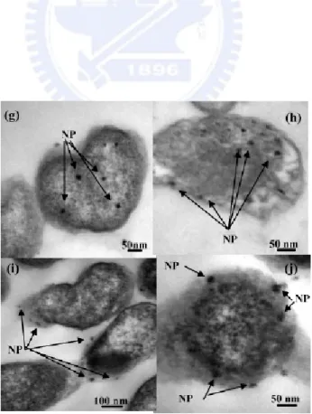
very body knows, the morphology and the dopant concentration of ZnO nanostructures can be well controlled by tuning the growth conditions. ZnO nanoparticles are believed to be nontoxic, biosafe, and possibly biocompatible, and have been used in many applications in our daily life, such as drug carriers and cosmetics. In order to study toxicological impact of ZnO nanoparticles, Brayner et al. first added macromolecules on the ZnO nanoparticles. Then, they studied of biocidal effects and cellular internalization of ZnO nanoparticles on Escherichia coli bacteria. These results showed that lower concentrations of ZnO nanoparticles did not induce any damage. Cellular internalization of these nanoparticles was observed in the Figure 2.14. [47]
Roselli et al. and Huang et al. get the similar result to prove that ZnO is a biosafe material.[48] Furthermore, Wang proved that ZnO wires are belong to biodegradability. [49] They have conducted a systematic study on the etching and dissolving behavior of ZnO NWs in various solutions with moderate pH values, including deionized water, ammonia, NaOH solution, and horse blood serum. The result shows that ZnO can be dissolved by deionized water (pH = 4.5–5.0), ammonia (pH = 7.0–7.1, 8.7–9.0) and NaOH solution (pH = 7.0–7.1, 8.7–9.0). The study of the interaction of ZnO wires with horse blood serum shows that the ZnO wires can survive in the fluid for a few hours before they eventually degrade into mineral ions. The results of this study are of great significance. The SEM results are shown in the Figure 2.15. First, biosensors made of ZnO nonmaterial have a certain time to perform a device function. Secondly, once completing the corresponding service, the ZnO wires can eventually dissolve into ions that can be completely absorbed by the body and become part of the nutrition. The biodegradability and biocompatibility of ZnO NWs would allow their use for in vivo biosensing and biodetection.
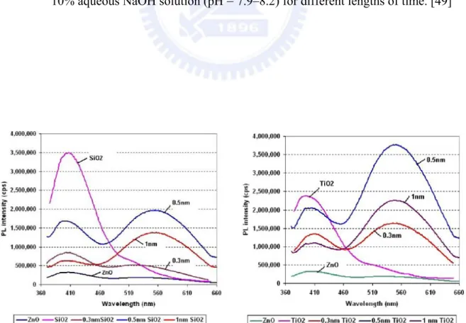
Generally, ZnO is one luminescent material due to its defects. ZnO quantum dots can enhance the intensity of luminescent emission for bio-image. Wu and co-workers reported that ZnO quantum dots can be used to bio-image by surface modifications. [50] They used Si
gel and TiO2 to combine with the ZnO. After surface modifications, the samples could be obtain strong visible emission with different thickness, as shown in Figure 2.16. This result showed ZnO quantum dots were suitable in the bio-image applications.
Bio-sensor based ZnO on is a challenging issue. Zhang et al. developed a reagentless uric acid (UA) biosensor based on uricase immobilized on ZnO nanorods. [51] The ZnO nanorods derived electrode retained the enzyme bioactivity and could enhance the electron transfer between the enzyme and the electrode. This sensor showed a high thermal stability up to 85 ◦C and an electrocatalytic activity to the oxidation of uric acid without the presence of an electron mediator.
Figure 2.3 Energy levels of native defects in ZnO. [25]
Figure 2.4 Formation energies as a function of Fermi-level position for native point defects in ZnO.[26]
Figure 2.5 A ZnO nanowire dye-sensitized solar cell [28]
Figure 2.6 ZnO nanorods laser [29]
Figure 2.7 Schematic diagram showing the design and structure of the nanogenerator. [30]
Figure 2.8 Scheme of solution growth of highly oriented microtubular array of ZnO onto substrates [31]
Figure 2.10 PL spectra of ZnO nanotbues nanorods and nanorwires [33]
Figure 2.9 (a) Top view SEM iamge and (b) HRTEM images of the sample grown for 1 h. [32]
Figure 2.11 TEM characterization of ZnO-Al2O3 core-shell nanowires. Scale bar (a) 50 nm (d) 5nm [44]
Figure 2.12 Arrays of ZnO nanowires and GaN nanotubes. Shown are SEM images of the ZnO nanowire template arrays (a), and the resulting GaN nanotube array (b). Inset in a shows cross-sections of the ZnO nanowires. [44]
Figure 2.14 TEM micrographs of E. coli thin sections (NP = ZnO
nanoparticles) (g-j) ZnO nanoparticles (10-3 M) internalization.[47]
Figure 2.16 Photoluminescence spectra of SiO2 and TiO2 –coated ZnO [50]
Figure 2.15 SEM images of a ZnO wire that has interacted with horse blood serum diluted in 10% aqueous NaOH solution (pH = 7.9–8.2) for different lengths of time. [49]
Chapter 3
Experimental materials and methods
3.1 Flow chart of experimental procedure Alumina precursor (nanoparticles and sol)
Synthesized ZnO nanostructure (rods, wires, tubes)
Coating alumina on the ZnO nanostructure
Rapid thermal annealing at 200oC ~ 800oC in N2 and O2 atnosphere
Characterization and Analysis
SEM
3.2 ZnO thin films formation
The ZnO thin films (~100 nm) were deposited on 4 in. diam Si substrates by radio frequency (rf) magnetron sputtering using 99.99% ZnO as the target. The growth chamber was evacuated by a turbo pump and a mechanical pump. The gas mole ratio of oxygen to argon (OMR) was varied in the range of 5%. The silicon substrates were cleaned by the usual semiconductor technology before loading into the chamber. The sputtering conditions were optimized at a substrate temperature of 50°C, an rf power of 50 W, a sputtering pressure of 10 mTorr, and a sputtering time of 40 min.
3.3 Wet-chemical growth of ZnO nanorods and nanotubes
Zinc nitrate hexahydrate (Zn(NO3)2 6H2O) was used as zinc precursors to synthesize ZnO nanorods (ZNs) and nanotubes (ZTs). Methenamine (C6H12N4), also called hexamethylenetetramine (HMT), is a highly watersoluble, non-ionic tetradentate cyclic tertiary amine and used to comply simultaneously with the precipitation of the divalent post-transition metal Zn2+ ions, the nucleation growth of its stable oxide form, zincite ZnO. Two kinds of substrates, one Si and the other Si coated with ZnO film, were also used. An equimolar (0.02M) aqueous solution of Zn(NO3)2.6H2O and HMT was prepared in a bottle. Subsequently, substrates were placed inside the aqueous solutions and heated in the temperature range of 55–95 oC for 0.1–48 h. Usually, ZnO nanorods were grown at 75oC and ZnO nanotubes were grown at 95oC. After that, the substrates were removed from the aqueous solutions, rinsed with distilled water, and dried at roomtemperature overnight.
Following the sol–gel porous alumina templating method proposed by Martin et al.5 M ammonia was added to an aqueous alumina nitrate solution (0.4 M) at room temperature. Then, the solution was controlled to the pH = ~10 to form hydrated precipitate. After the hydrated precipitate was formed, it was centrifugally separated and washed several times with distilled water. The precipitate was dry in the oven for 12 hours. Then, the alumina nanoprticles can be obtained. On the other hand, the precipitates were put into 100 ml D. I. water. Then, the solution was peptized with nitric acid and control the pH = 6.5 ~ 7.5. A translucent, homogeneous and stable sol was obtained.
3.5 Synthesis and thermal treatment of alumina/ZnO core/shell structure
The ZnO nanorods were subsequently immersed in the precursor sol of Al+3 to grow an alumina shell on the ZnO nanorods at 80oC for 1 hr. The thickness of alumina shell on the ZnO nanorods can be modulated by controlling reaction parameters, such as reaction time and temperature. The alumina-coated ZnO nanocables were obtained.
The alumina nanoparticles was dispersed in the water solution by ultra-sonication and adjusted to pH 8.0 with ammonia. The nanoparticles with pseudoboehmite phase (γ-AlO(OH) will absorb OH- ions to form –OO- Al – OH2+ on the surface. Then, the ZnO nanotubes will react with –OO- Al – OH2+ precursor to deposit alumina nanoparticles on the ZnO nanotubes after immersed into the solution at 120oC for 1 hr.
After washing the alumina-coated ZTs with distilled water, rapid thermal annealing (RTA) was performed for 20 minutes under oxygen and nitrogen atmospheres. The annealing parameter: raising temperature , 10 oC/min to 200oC, 400oC, 600oC and 800oC and holding the temperature. The samples were inserted into the tube at fix temperature and hold during 20 minutes. Finally, the samples were drawn out after 20 minutes.
3.6 Characterization of ZnO and alumina materials
An X-ray diffractometer (M18XHF, MAC Science, Tokyo, Japan) was used to examine the crystalline phase of the synthesized compounds with a scanning rate of 4o (2θ) per min over a 2θ range of 10~70o. Cu Kα radiation was used and the operating voltage was 50 kV. The growth morphology of the ZnO nanorods was examined by field emission scanning electron microscopy (FE-SEM, JOEL-6700). The samples were analyzed with a field emission transmission electron microscope (TEM, JEOL 2100F) with energy dispersive x-ray spectroscopy (EDS) operated at 200 keV. Room-temperature PL measurements were performed with a 325 nm He–Cd laser with an excitation power of 25 mW. The emitted luminescence was detected with a 0.32 m spectrometer with a charge-coupled device detector. The focused spot size of the He–Cd laser was estimated to be about 200 μm in diameter. The Fourier Transform Infrared spectrometry (FTIR, PerkinElmer spectrum 100 was use to examine the alumina bonding during the thermal treatment process. A scanning number was 4 times: the resolution was 4 cm-1: the scanning range was 450~4000 cm-1. The 27Al MAS NMR was used to examine the chemical shift of alumina-coated ZnO nanorods scraped from the Si substrate using a Bruker Dsx400wc NMR Spectrometer. X-ray photoelectron spectroscopy (XPS) was used to evaluate Al-O chemical binding states. The XPS analyses were performed on a Kratos AXIS Ultra with a monochromatic Mg X-ray source at 150W.
Chapter 4
Tunable growth of ZnO nanorods synthesized in aqueous solutions
at low temperatures
4.1 Introduction
One-dimensional ZnO nanocrystals have been extensively studied because of their promising chemical and physical properties,[52] and show potential applications in manufacturing electronic and optoelectronic devices.[53.54] In the past, a variety of methods have been employed, including vapor phase transport, metal-organic chemical vapor deposition to grow arrayed nanorods and nanowires of ZnO from aqueous solutions. Recently, many wet-chemical approaches have been developed to prepare oriented arrays of ZnO nanorods on polycrystalline (or single crystalline) substrates from aqueous solutions. Choy et al. reported that the buffer layer of dip-coated ZnO nanoparticles can effectively reduce the mismatch between the Si substrate and the ZnO nanorods.[55] Our previous report also suggested that on a Si wafer coated with a ZnO film, well-aligned ZNs with different aspect ratio can be grown along the [0002] direction on the Si aubatrate coated with ZnO film (ZnOf/Si substrate).[56] All the observations reveal that the undercoating ZnO film plays a very important role in the development of ZNs. However, no systematical studies have been performed up to now. Therefore, the growth condition of the ZnO nanorods was first studied. Then, we investigate the effect of annealing treatment of the undercoating ZnO film on the growth behavior of ZNs. Furthermore, it was found that the ZNs can be selectively grown on
a patterned ZnO film which can serve as seeds to modify the morphology of ZNs by controlling the annealing condition of the coated ZnO film on any substrates.
4.2 ZnO nanorods with different growth parameters
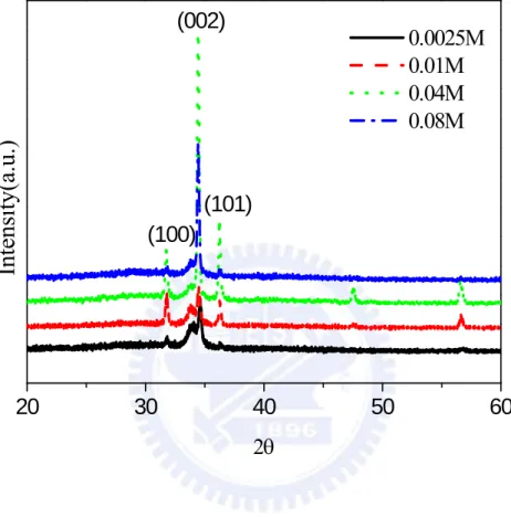
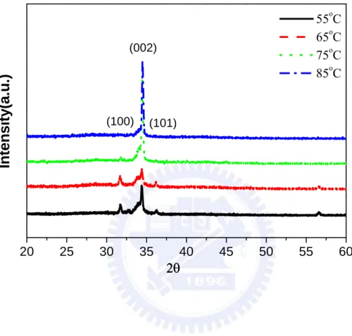
Figure 4.1 shows the morphology of the ZNs with different concentrations ( 0.0025M、 0.01M、0.004M and 0.08M) at 75oC for 10 hours. When the concentration was 0.0025M, it could be observed few and small ZNs. With increasing the concentration, the density of the ZNs would be increased. When the concentration was over high (0.08M), the morphology of ZNs would look like nanorod film, indicating too high density, as shown in the figure 4.1(d). The diameter of the ZNs would be reduced with the decrease of the solution concentrations. Because low Zn+ concentration would reduce the growth rate of the ZNs, small ZNs were obtained. The X-ray diffraction patterns (XRD) in Fig. 4.2 presents the growth orientation and crystalline of the ZNs. It can be obtained three main peaks ( 31.7, 34.4 and 36.2) which fit the wurzite structure by JCPDs card. When the solution concentration was 0.0025M and 0.01M, the (002) peak intensity was weak, indicating that the crystalline of the ZNs was not strong.
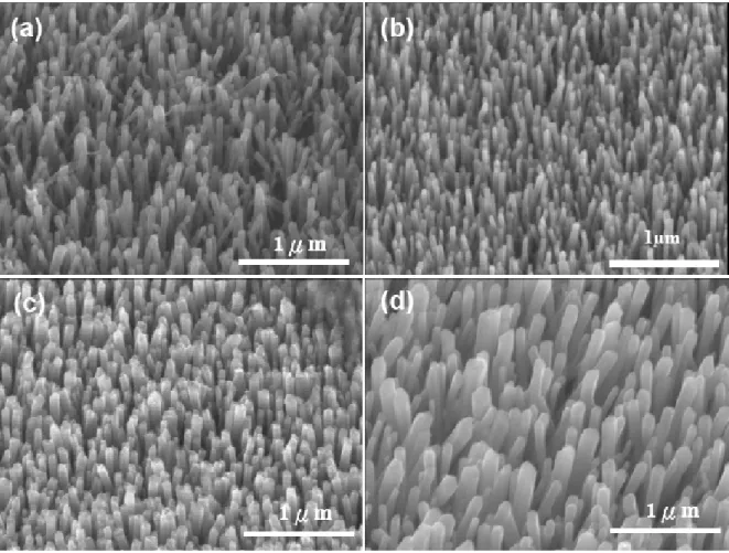
Figure 4.3 shows the morphology of the ZNs with growth temperature ( 55 oC, 65 oC, 75 oC and 85 oC) in 0.04 M for 10 hours. When the growth temperature increased from 55 oC to 85 oC, it could be observed the average diameter of the ZNs increased from 30 nm to 120 nm. When the growth temperature was below 50oC, it can not be obtained any ZNs because chemical reaction do not overcome the active energy barrier. The (002) intensity of the ZNs was weak when the growth temperature was 55 oC and 65 oC, as shown in the Fig. 4.4 Moreover, the (100) peak was so obvious, indicating that some ZNs were not grown vertically on the substrate. When the growth temperature was increased to 75 and 85 oC, the ZNs owned high crystalline and single orientation.
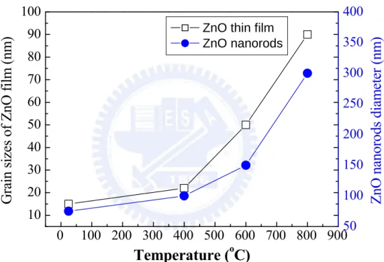
Si substrate (ZnOf/Si) at different annealing temperatures. It was found that that the grain size of the ZnO film on Si substrates becomes larger and the surface morphology becomes rough with the increase of annealing temperature. Furthermore, it can be observed in Fig. 4.5(b) that many abnormally large ZnO grains were grown on the ZnOf/Si substrate annealed at 800oC. Furthermore, according to our previous study, it was found that the diameter of ZnO nanorods was affected by the concentrations of the aqueous solution. Therefore, the same concentration of the precursors (0.01M) was used in this work to avoid the effect of solution concentration.
4.3 Patterned growth of the ZnO nanorods
Figure 4.6 shows the SEM images of the ZNs grown on the patterned ZnOf/Si annealed at different temperatures, where the patterned ZnO film on Si substrate was fabricated by the photolithography and etching process. As the patterned ZnOf/Si substrate was placed into the aqueous solution to grow ZNs, well-aligned ZNs are grown on the designed substrate, as shown in Fig. 4.6(a), and this demonstrates the selected growth behavior of the ZNs. Figure 4.6(b) shows the surface images of large-scale arrayed ZnO nanorods grown on the patterned ZnOf/Si at room temperature and the ZnO nanorods have a well-defined hexagonal plane with a homogeneous diameter. Although the ZnOf/Si substrate was patterned , nucleation of the nanorods was not correlated with the substrate patterning and subsequent growth of the ZnO grains was also unaffected by patterning. However, as the patterned substrates were first annealed at 600oC and 800oC, prior to the growth of the ZNs in the solution at 75oC, we found that the morphology of the ZNs was markedly changed, as shown in Fig. 4.6(c) and (d), especially for the ZnOf/Si annealed at 800oC. Furthermore, the dimension of ZNs increases with increasing annealing temperature. The average dimension of the ZNs is 20 nm and 300 nm in diameter for the ZnOf/Si at room temperature and annealed at 800oC, respectively. When compared with the AFM images of ZnO film on Si substrate shown in Fig. 4.5, this
seems to imply that the growth behavior of the ZNs is correlated with the grain size of the ZnO film sputtered on Si substrate, as illustrated in Fig. 4.7. Furthermore, there exists a critical temperature around 400oC, and above that, the ZNs are rapidly grown and become larger in diameter.
4.4 The relation between ZnO film and ZnO nanorods
Figure 4.8(a) shows the TEM bright-field (BF) image of the aligned ZNs grown on the annealed ZnOf/Si substrate at 600oC. It was observed that most of the ZNs were grown along the direction perpendicular to the ZnOf/Si substrate. The TEM dark-field image marked with arrows in the Fig. 4.8(b) reveals that there exists a close relationship between ZNs and ZnO film. Both ZNs and ZnOf on Si substrate were grown along the same direction of [0002] and are coherent, as demonstrated by the selected-area electron diffraction pattern (SAED) (inset of Fig. 4.8(b)). In addition, as one observes the interface between ZNs and ZnOf/Si shown in Fig. 4.8(c), the HR-TEM image (magnified from the marked area in Fig. 4.8(a)) reveals that both the ZNs and ZnO film have identical parallel lattice fringes. This indicates that the ZNs seem to nucleate from the concave tip near the grain boundary (marked as lines) between two ZnO grains in ZnO films because it (near the concave tip) has a higher surface energy. A detailed discussion can be referred to Ref. 5.
As the ZnOf/Si substrate was annealed at a higher temperature of 800oC, a low-magnification TEM image of the ZNs was shown in Fig. 4.9(a). The HR-TEM image of the ZNs marked with the box in Fig. 4.9(a) was further illustrated in Fig. 4.9(b) where some nanorods are merged together to form a larger ZN along similar growth direction [0002].[57] The selected area diffraction pattern (SADP) (shown in the inset of Fig. 4.9(b)) reveals that the diffraction spots were split with several different angles. This suggests that the larger ZNs are not perfectly single-crystalline and consist of three ZNs, as illustrated in Figs. 4.9(c), (d)
and (e), with a slight misalignment between the nanorods. Therefore, the growth behavior of the larger ZnO nanorods can be considered from the direct combination of a small number of individual nanorods having a similar orientation.[58]
4.5 Summary
We demonstrated that the growth of patterned ZnO nanorods can be controlled by changing the annealing conditions of the ZnOf/Si substrates. When the ZnOf/Si substrate was annealed above a critical temperature to promote the crystallization of ZnO phase, both ZNs and ZnOf on Si substrate were found to become crystallographically matched. In this work, it reveals that the ZNs seem to preferentially nucleate from the cup tip near the grain boundary between two ZnO grains in the ZnO film. However, a higher annealing temperature may lead to the formation of a larger ZnO crystal due to coplanar coalescence behavior of several individual ZnO nanorods.
20
30
40
50
60
(100)
(002)
(101)
Intensity(a.u.)
2θ
0.0025M
0.01M
0.04M
0.08M
Fig. 4.4 XRD analysis of the ZNs synthesized in different growth temperature. 20 25 30 35 40 45 50 55 60 (101) (100) (002)
Intensity
(a.u
.)
2θ 55oC 65oC 75oC 85oCFig. 4.5 AFM images of (a) as-grown ZnO films and (b) annealed ZnO film at 800oC.
(a)
(b)
(a)
Fig. 4.6 SEM images of the ZnO nanorods (a) grown on the patterned ZnOf/Si, (b) grown at 1μm 1μm 1μm 1μm
(c)
20μm 50nm 500nm 500nm(d)
(a)
(b)
(c)
0
100 200 300 400 500 600 700 800 900
10
20
30
40
50
60
70
80
90
100
ZnO thin film ZnO nanorods
Temperature (
oC)
Gr
ain
sizes of Z
nO
film
(
nm
)
50
100
150
200
250
300
350
400
Z
nO
nanorods diam
ete
r (nm
)
room temperature, and grown on the annealed ZnOf/Si at (c) 600oC and (d) 800oC.
Fig 4.8 (a) TEM bright-field and (b) dark field images of the aligned ZNs grown on ZnOf/Si
substrate annealed at 600oC. A corresponding diffraction pattern is shown in the inset
of Fig. (b) for the selected single nanorod. (c) A high-resolution TEM image of (a)
showing the interface between ZNs and ZnOf.
(002) (110) 50nm 20nm
(a)
(b)
(c)
(b)
(a)
(c)
Fig. 4.9 (a) Showing the low-magnification TEM images of ZnO nanorods grown on the
annealed ZnOf/Si at 800oC. (b) HRTEM images of the ZnO nanorods marked in the
frame of (a) along with split diffraction pattern in the inset. HRTEM image of (c)
left, (d) middle and (e) right side of the larger nanorod, showing the larger ZnO
nanorod seems to be composed of three ZNs.
20nm 200nm
(c)
(c)
(d)
(e)
(b)
(a)
Chapter 5
Growth behavior and microstructure evolution of ZnO nanorods
grown on Si in aqueous solution
5.1 Introduction
One-dimensional (1D) semiconductor nanostructures have been extensively studied for their potential applications in manufacturing electronicand optoelectronic devices [59]. Zinc oxide (ZnO) is an important electronic and photonic material because of its wide and direct band gap (ΔEg 3:37 eV) material [60]. The strong exciton binding energy of ZnO (60 meV) is much larger than that of GaN (25 meV), which can ensure an efficient exciton emission at room temperature. Recently, highly oriented nanorod arrays of ZnO nanostructures have demonstrated their potential applications in manufacturing electronic and optoelectronic devices [61,62]. Various methods, including chemical, electrochemical, and physical deposition techniques have been employed to synthesize 1D ZnO nanostructures such as catalytic growth via the vapor–liquid–solid (VLS) epitaxial method [63] and metalorganic-chemical vapor deposition (MOCVD) [64]. However, those methods are expensive and energy consuming processes since they are operated under extreme conditions. On the other hand, many wet-chemical approaches have been used for large oriented arrays of ZnO nanorods on polycrystalline (or single-crystalline) substrates from aqueous solutions [65]. It is well conceived that the preparation of ZnO via solution chemical routes provides a promising option for large-scale production of these materials. Recently, Vayssieres et al. has proposed a novel theoretical concept, called ‘‘purpose-built materials’’, to grow arrayed
nanorods and nanowires of ZnO fromaqueo us solutions [66]. Such an approach does not require any template, membrane or applied external field to create anisotropic nanoparticles. However, it is worth noting that without suitable treatment on the substrate, highly oriented ZnO nanorods grown on a Si wafer have been rarely achieved due to the larger mismatch (~40%) between the substrate and the ZnO nanorods. Yamabi et al. reported that without undercoats on the surface, clusters of spindle-shaped hexagonal crystallite with diameters of 0.5–1.0 mm were scattered over the surface of a silicon wafer, but highly aligned arrays of ZnO nanorods with diameters of 20–100nm can be developed on Si substrate undercoated with Zn(Ac)2 and annealed at 500 oC [67]. Recently, Choy et al. also found that high-quality ZnO nanorods were successfully grown on a Si wafer by a wet-chemical process at 95 oC for 6 h, where the Si wafer was dip-coated with 4 nm sized ZnO nanoparticles as a buffer and seed layer prior to crystal growth [68]. These observations reveal the importance of surface characteristics or treatment on the growth of well-oriented ZnO nanorods in aqueous solution. However, little investigation has paid attention to the growth behavior of such ZnO nanorods, in particular to tailor their orientation onto the substrates that can be used to control the structure morphology and optoelectronic properties. Therefore, in this work, a simple wet-chemical method was used to study the growth behavior of both scattered and aligned ZnO nanorods on Si by monitoring the average aspect ratio of ZnO nanorods as a function of growth time in aqueous solution. By controlling the experimental conditions, scattered or well-aligned ZnO nanorods with different aspect ratios can be obtained. Moreover, high-resolution transmission electron microscopy (HRTEM) was performed to investigate the microstructure evolution of both ZnO nanorods.
5.2 Phase and morphology of ZnO nanorods grown on different substrates
behavior of ZNs in the precursor solution at different temperatures of 55–95 oC for several hours. No ZNs were observed below 50 oC, indicating that a thermal barrier for the growth of ZNs cannot be overcome. Above 95 oC, ZNs cannot be synthesized because the reaction temperature is near the melting point of the aqueous solution. Fig. 5.1 shows the SEM images of the as-synthesized ZNs grown on these two kinds of substrates at 75 oC for 10 h in the 0.02M solution. As shown in Fig. 5.1(a), ZNs with dimensions of 7~10 mm in length and 0.5~1 mm in diameter were scattered on the Si substrate. On the other hand, high densities of well-aligned ZNs with dimensions of 20–200nm in diameter and up to several mm in length were obtained when ZNs were grown on ZnOf/Si as shown in Fig. 5.1(b). It seems to imply that the formation of well-aligned ZNs on a pure Si substrate is difficult because a large mismatch (~40%) exists between ZnO and Si. Hence, this would retard the nucleation of ZnO nanorods on Si substrate. This observation strongly reveals the importance of the substrate characterization on the growth behavior of ZNs in the aqueous solution.
The X-ray diffraction patterns (XRD) in Fig. 5.2 show that the ZnO crystal phase starts to appear at 50 oC and is well crystallized above 65 oC. A strongly oriented peak can be indexed as the wurtzite ZnO at 75 oC in 0.02M aqueous solutions for the ZNs grown on Si and ZnOf/Si substrate. However, it should be pointed out that a remarkable difference in XRD patterns exists between these two substrates. As shown in Fig. 5.2(a), the diffraction peaks were indexed as (1 0 0), (0 1 0) and (1 0 1) planes of ZnO for the ZNs grown on Si substrate. On the other hand, Fig. 5.2(b) illustrates that the strongest diffraction peak corresponding to the (0 0 2) plane of ZnO was detected when the ZNs were grown on ZnOf/Si substrate. These observations obviously reveal that there exists different growth behavior between (1 0 0)-oriented (called scattered) ZNs on Si and (0 0 2)-oriented (called aligned) ZNs on ZnOf/Si.
ZnO has a hexagonal lattice with a c/a axial ratio of 1.602 [69]. The most commonly observed morphologies of ZnO are either rod-like or needlelike crystals, especially the prepared ZnO in aqueous solution because of anisotropic crystal growth. The TEM bright-field (BF) image and corresponding selected-area diffraction pattern (SADP) of the scattered ZNs are shown in
Figs. 5.3(a) and (b), respectively. The SADP in Fig. 5.3(b) clearly indicates that the scattered
ZNs were grown along the ٛ[0110] direction. This result is also consistent with the XRD −
analysis that the ZNs are preferentially oriented along the ٛ[011 0] direction. A close − examination of the SADP shows the split of diffraction spots and extra diffraction spots,
located halfwaybetween the central (0 0 0) spot, the 0002 spots and f {0110} spots. However, − no Morie’ fringes were observed in the corresponding HRTEM in Fig. 5.3(c) so that double diffraction can be neglected in this study. Since the crystallographic phase of these ZNs belongs to wurtzite structure with a space group of P63mc, it easily appears as a characteristic ‘‘zigzag’’ structure [70,71], so-called ‘‘superlattice diffraction’’, corresponding to the observed extra spots in the SADP. It seems to imply that the crystal structure of the scattered ZNs was constituted from many tiny areas such as domains or mosaic texture according to the disoriented few degrees in SADP. It is well known that a crystal with mosaic structure does not have its atoms arranged on a perfectly regular lattice extending from one side of the crystal to the other; instead, the lattice is broken up into a number of tiny blocks, each slightly disoriented one froman other. Within these tiny blocks, there exists a structural mismatch at the interface between these domains [72], as in this case with 1–21 difference in the SADP. Furthermore, the HRTEM image in Fig. 5.3(c) recorded from the scattered ZNs reveals that there seemto be two types of lattice fringes in this HRTEM image: one with wave-like fringes (as arrowed in Fig. 5.3(c)) and the other with straight fringes. This variation of lattice fringes as marked with arrows seems to be caused by these two types of crystal arrangements. Fig.
to the scattered ZNs, most of the ZNs were grown along the direction perpendicular to the ZnOf/Si substrate. A higher magnification in Fig. 5.4(b) indicates that the lattice fringes are perpendicular to the longitude direction of the ZNs, and the singular fringe spacing is about 0.51 nm, which is nearly consistent with the c-axis parameter in hexagonal ZnO structure (c=0.521nm in ZnO structure). This demonstrates that the [0 0 0 2] direction is the preferred growth direction for the well-aligned ZNs. In addition, as one pays attention to the interface between ZNs and ZnOf/Si shown in Fig. 5.4(c), it was observed that the well-aligned ZNs seemto be nucleated from the cup tip near the grain boundary between two ZnO grains in ZnO film. The lattice image at the joint of the interface, shown in the inset of Fig. 5.4(c), clearly indicates that the lattice fringes near the interface of ZnO grains in ZnO film are continuous without any cracks. The formation of the cup shape around grain boundaries between two ZnO grains is supposed to be correlated with the solution reaction during the nucleation and growth of ZNs. This implies that the cup tip probably becomes a preferential nucleation position for the well-aligned ZNs grown on ZnOf/Si. However, in addition to (0 0 0 2) fringes, some ZNs with white lines dissecting the ZNs can be identified as marked with arrows in Fig. 5.5 that is probably due to faster stacking and the instability of the polar (0 0 2) plane in ZnO. These kinds of planar defects are easily developed at a higher growth temperature, i.e. 90 oC, and can be considered as extrinsic stacking faults with insertion of an extra Zn-O layer parallel to the basal plane. It was worth noting that the presence of (0 0 0 1) stacking faults provides a possible diffusion path to modify its optoelectronic properties according to our study [73]. However, wellaligned ZnO nanorods without any planar defects can also be obtained in aqueous solution by controlling the experimental conditions.
5.4 Growth behavior of ZnO nanorods
conditions such as ion concentration in the solutions, reaction temperature and time, which can be elucidated by the change of the aspect ratio (AR=length/width) of ZNs. As illustrated
in Fig. 5.6, when the pure Si substrate was placed in the Zn-containing aqueous solution at 75
oC, it was found that in an initial growth stage of ZNs, prior to 0.2 h, no obvious ZNs can be detected. However, above that (0.2–0.3 h), SEM images (not shown here) show a small amount of ZNs with ~20 nm in diameter and ~60 nm in length that were randomly scattered on Si substrate. Although the SiO2 is probably formed on the Si substrate, a similar growth phenomenon is also observed for SiO2/Si substrate. This implies the importance of ZnO film coating on the nucleation and growth of aligned ZnO nanorods. Above 0.5 h, the aligned ZNs can be clearly obtained but the scattered ZNs start to preferentially grow along the longitude (c-axis) direction. With an increase of growth time, it can be observed that the growth of scattered ZNs becomes slower compared to that of the aligned ZNs. Especially above 5 h, it was found that the AR of the scattered ZNs changes little (9–11). Furthermore, with increasing growth time up to 15 h, the AR slightly decreases. This implies that the scattered ZNs do not further grow as expected despite extending growth time. As evidenced from the TEM BF image and corresponding SADP of ZNs shown in Fig. 5.7, it seems to reveal that more than two ZNs are self-assembled together to for a bundle in a coplanar manner using their side planes to forma large ZN as shown in Fig. 5.7(c) of the TEM dark-field (DF) image. This bundle of ZNs can be further transformed into another ZN with a larger dimension in diameter. In other words, the side crystal planes of the ZNs are able to glue together to forma larger crystal. This behavior is also called ‘‘oriented attachment’’ [74]. This observation may be used to explain the slight decrease in AR in the later growth stage (5–15 h). Consequently, the growth behavior of the scattered ZNs can be considered as a two-step growth mechanism. In contrast, as the ZnOf/Si substrate was used and immersed into the precursor solution for the growth of ZNs, it was found that in the initial growth stage (to 0:5), no aligned ZNs can be clearly observed fromthe ZnOf/Si substrates, but at 1h, a smaller AR was obtained for the
![Figure 2.4 Formation energies as a function of Fermi-level position for native point defects in ZnO.[26]](https://thumb-ap.123doks.com/thumbv2/9libinfo/8030586.161377/27.892.149.688.177.1070/figure-formation-energies-function-fermi-position-native-defects.webp)
![Figure 2.7 Schematic diagram showing the design and structure of the nanogenerator. [30]](https://thumb-ap.123doks.com/thumbv2/9libinfo/8030586.161377/29.892.198.621.159.665/figure-schematic-diagram-showing-design-structure-nanogenerator.webp)