國 立 交 通 大 學
電信工程學系
博 士 論 文
側向擴散金氧半電晶體之多諧波失真模型
及表面聲波氣體感測器之設計
Polyharmonic Distortion Model for LDMOS
Device and SAW Gas Sensor Design
研 究 生:邱佳松 (Chia-Sung Chiu)
指導教授:吳霖堃 (Lin-Kun Wu)
側向擴散金氧半電晶體之多諧波失真模型
及表面聲波氣體感測器之設計
Polyharmonic Distortion Model for LDMOS Device and SAW
Gas Sensor Design
研究生:邱佳松
Student:
Chiu-Sung
Chiu
指導教授:吳霖堃 博士 Advisor:
Dr.
Lin-Kun
Wu
國立交通大學
電信工程學系
博士論文
A Dissertation
Submitted to Institute of Communication Engineering
College of Electrical and Computer Engineering
National Chiao Tung University
in Partial Fulfillment of the Requirements
for the Degree of Doctor of Philosophy
in
Communication Engineering
Hsinchu, Taiwan
側向擴散金氧半電晶體之多諧波失真模型及表面聲
波氣體感測器之設計
學生: 邱佳松 指導教授: 吳霖堃 博士
國立交通大學
電信工程學系
摘要
本論文主要針對主動元件在不同佈局結構、非線性模型與感測領域進行分析與應 用。一般而言,半導體裡的主動元件,例如金氧半場效電晶體(MOSFET)或雙極性接面 電晶體(BJT),為無線通訊系統或感測系統中最重要的元件之一。其元件特性足以影響 應用系統裡的整體表現、價格與穩定性。而在一般無線通訊領域或基地台等遠距離的發 射器,大都以側向擴散金氧半電晶體(laterally-diffused MOS transistor)作為主要之放大元 件。在本研究中,首先提出了側向擴散金氧半電晶體之新型佈局樣式,利用圓形佈局樣 式以達到低開啟通道電阻(On-resistance)與小面積的元件佈局。依據實驗的量測結果,圓 形的佈局樣式因有較小的寄生電容與較高之轉導增益,所以有較高的截止頻率(fT)與最 大震盪頻率(fmax)。除了小訊號分析外,論文中也進行大訊號特性分析比較。而在研究的 量測結果,與傳統佈局樣式比較之下,圓形佈局樣式亦有較佳之大訊號特性表現。 除了功率元件佈局設計外,主動元件之非線性特性模型在設計與應用上也相形重 要。在研究中,我們分析了多諧波失真模型,並且利用此模型模擬出主動元件的非線性
行為。經由晶圓級非線性向量網路分析儀所萃取出之多諧波失真模型,在1.9GHz的操作 頻率點,射頻側向擴散金氧半電晶體的大訊號特性模擬結果與傳統功率量測的結果一 致,並且無需另外進行電腦最佳化與曲線近似處理。 論文中的另一部分,我們利用了半導體中的主動元件與表面聲波(Surface acoustic wave, SAW)延遲線元件進行感測器之設計與分析。研究中針對了元件的特性,進行此感 測器之電性測試與氣體感測結果分析。在感測的實驗結果中,表面聲波感測器在 50x103ppm的酒精氣體濃度裡,其中心訊號有近10kHz的訊號漂移。研究的最後並針對感 測元件與系統,提出改進及可能的發展方向。
Polyharmonic Distortion Motel for LDMOS Device and
SAW Gas Sensor Design
Student: Chia-Sung Chiu Advisor: Dr. Lin-Kun Wu
Department of Communication Engineering
National Chiao Tung University
Abstract
This dissertation presents the layout design, nonlinear modeling and sensing application in terms of active device. The active device, such as MOSFET or BJT in semiconductor, is one of the most important components of a wireless communication or sensing system generally. It plays a significant part in determining the overall performance, cost, and reliability of these application systems. In the world of RF wireless communications, the base-stations and long range transmitters use silicon laterally-diffused MOS (LDMOS) high power transistors almost exclusively. To achieve lower on-resistance and a more compact device size, this study adopted an annular structure in the layout design. According to the measurement results, the smaller drain parasitic resistance in the annular structure could be the key factor for improving ft and fmax. In additional to the small-signal analysis, the large-signal characteristics,
such as power gain and power added efficiency, were also improved compared to the transitional structure of LDMOS.
In addition to high power device design, the behavior model of the nonlinear characteristics for active device is also crucial. In this study, we analyze the polyharmonic distortion model (PHD) and use this model to predict the nonlinear behavior of active device. By way of the PHD model extracted using on-wafer nonlinear vector network analyzer (NVNA), the large-signal validation of this model also shows a good match with measurements at 1.9 GHz without optimization and curve fitting.
In another part of this thesis, we discussed and analyzed the sensor design completely using CMOS active device and SAW delay-line device. Their electrical characteristics are evaluated as well as vapor sensing results. The sensing experimental results show that the maximum oscillation frequency shift between gas on and off is approximately 10 kHz with 50 x 103 ppm alcohol vapor concentration. Conclusions on the sensing device and system, and recommendations concerning potential improvements of these components are discussed, finally.
誌 謝
回想博士班的求學過程中,在師長、前輩、親友與朋友的支持下,雖
然辛苦但也有著滿滿的回憶。首先,最先感謝的是我的指導教授—吳霖堃
老師,在這幾年辛勤與耐心的指導下,每當我陷入研究困境與人生泥沼時,
都能適時地鼓勵與啟發學生,讓我獲益匪淺;老師的嚴謹治學精神及豁達
人生觀,也深深地影響著我。其次,感謝國家奈米元件實驗室研究員黃國
威博士,您的支持與協助,在我的求學與研究的過程中,幫助我克服許多
困難,在此表達由衷的感謝。另外口試期間承蒙交通大學張志揚教授、周
復芳副教授及中華大學高曜煌教授撥冗指正與建議,使本論文疏漏之處得
以匡正,在此致上最深謝意。
特別感謝中原大學電子系的鄭湘原老師,感謝您長久以來對學生的支
持與鼓勵,每當學生面臨研究困惑與徬徨時,總是不吝提供意見並給予協
助,在此由衷地表示謝忱。並感謝中原大學電子系先進電子元件研究室的
學弟學妹們,謝謝你們在實驗方面的協助。
感謝國家奈米元件實驗室高頻技術組的陳坤明博士、吳師道博士、生
圳學長、文林、書毓、裕民、國祥、柏源、治華、汶德、榮彥的打氣與協
助,使得原本枯燥的研究生活,增添了許多歡樂的氣氛。另外也特別感謝
卓銘祥博士,讓我在求學與工作生活中,留下了不少的美好回憶。
感謝我的父親—邱民文先生和母親—黃月美女士,謝謝您們一直對我
的支持、關心與包容,有您們對我的支持,才能使我在忙碌的工作之餘,
得以順利完成學業。最後,感謝我的太太—滿嬌,在我漫長的求學期間給
我的鼓勵與支持,因為有妳在背後無怨無悔對家庭的照顧與付出,才能使
我無後顧之憂的專注於論文研究,使得論文得以完成。當然也要感謝我的
兩個小寶貝—暐博與湘芸,讓爸比在工作與學業壓力下,只要看到你們可
愛的笑容,就足以溶化肩頭上的負荷。
最後,要感謝的人太多了,無法一一列舉。在此僅以滿懷感謝與感恩
的心,對所有幫助過我的人,致上萬分的謝意,願與你們分享這份喜悅。
邱佳松 謹誌
于 新竹交通大學
中華民國九十八年七月
Contents
Chinese Abstract... i
English Abstract ... iii
Acknowledgements... v
Contents... vii
List of Figures ... ix
List of Table ... xii
Chapter 1 Introduction
1.1 Introduction ... 1
1.2 Motivation ... 2
1.3 Dissertation Organization ... 4
Chapter 2 Characterization of Annular-structure RF LDMOS
2.1 Introduction ... 6
2.2 Annular-structure RF LDMOS ... 7
2.2.1 Device Design and Fabrication... 7
2.2.2 DC Characteristics ... 8
2.2.3 High-frequency Characteristics ... 9
2.3 Annular-structure and Square-structure Comparison ... 11
2.3.1 Effective Transconductance Evaluation ... 11
2.3.2 Capacitances versus V
GSand V
DS... 12
2.3.3 High-frequency Characteristics and Power Performance... 13
Chapter 3 RF Transistor PHD Modeling
3.1 Introduction ... 27
3.2 Polyharmonic Distortion Model Theory... 29
3.3 RF Active Device Power Characteristics... 35
3.3.1 Measurement Setup and On-wafer Calibration ... 35
3.3.2 Linearity and Power Performance ... 36
3.4 Summary ... 37
Chapter 4 Sensing Application
4.1 Introduction ... 47
4.2 Basic Sensing Mechanism ... 48
4.3 Circuit Design and Experiments ... 50
4.3.1 Device Design and Fabrication... 50
4.3.2 Sensing System ... 53
4.4 Results and Discussion... 54
4.5 Summary ... 55
Chapter 5 Conclusion and Recommendations
5.1 Conclusion... 66
5.2 Recommendations for Future Work... 68
Reference ... 69
Appendix 1 ... 80
List of Figures
Chapter 1
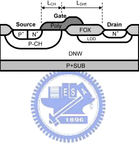
Fig. 1-1 A cross section of traditional high-power LDMOS transistor. ... 5
Chapter 2
Fig. 2.1 The traditional LDMOS layout structure:
(a) fishbone and (b) square... 16
Fig. 2.2 The die photo of annular-structure RF LDMOS. ... 17
Fig. 2.3 The cell layout of the annular-structure RF LDMOS... 18
Fig. 2.4 Schematic cross section of the LDMOS transistor... 19
Fig. 2.5 A simple equivalent circuit model of the LDMOS... 20
Fig. 2.6 (a) Output and (b) subthreshold characteristics of LDMOS
transistors for different layout structures. ... 21
Fig. 2.7 Extracted C
GS+C
GBand C
GDversus gate voltage with different
drain biases for square-structure LDMOS transistor ... 22
Fig. 2.8 Extracted C
GS+C
GBand C
GDversus gate voltage with different
drain biases for annular-structure LDMOS transistor... 23
Fig. 2.9 Schematic view of layout structure and current distribution in
RF LDMOS. (a) square structure and (b) annular structure ... 24
Fig. 2.10 Cutoff frequency (f
T) and maximum oscillation frequency (f
max) of
annular-structure LDMOS at V
D= 20V, and V
G= 1, 2, 3 V... 25
Fig. 2.11 Output power and efficiency versus input power at 1.9 GHz,
V
D= 20V, and V
G= 2.5 V with different layout structure. ... 26
Chapter 3
Fig. 3.1 The concept of describing functions... 38
Fig. 3.2 The harmonic superposition principle. ... 39
Fig. 3.3 On-wafer PHD model extraction system... 40
Fig. 3.4 Nonlinear vector network analyzer (NVNA). ... 41
Fig. 3.5 Measured and simulated results of the gain for annular-structure
and square-structure LDMOS transistors with width 80 μm at
1.9 GHz. ... 42
Fig. 3.6 Measured and simulated results of the IM distortion for
annular-structure LDMOS transistors with total width length 80
μm at 1.9 GHz. ... 43
Fig. 3.7 (a) Simulated and (b) measured results of the B2 wave
in time domain... 44
Fig. 3.8 Measured results of gain circle for annular-structure LDMOS
transistors from load-pull system with total width length 80 μm
at 1.9 GHz. ... 45
Fig. 3.9 Simulated results of gain circle for annular-structure LDMOS
transistors from PHD model with total width length 80 μm
at 1.9 GHz. ... 46
Chapter 4
Fig. 4.1 A diagram of the sensor device... 56
Fig. 4.2 The photo of SAW device: (a) without cap and (b) with cap... 57
Fig. 4.3 The schematic of sensor system... 58
Fig. 4.4 Two port amplifier: (a) circuit schematic and
Fig. 4.5 The design flow of sensor circuit... 60
Fig. 4.6 The photo of the circuit... 61
Fig. 4.7 Experimental sensing system in this study. ... 62
Fig. 4.8 The power measurement of oscillator... 63
Fig. 4.9 The phase noise measurement of oscillator. ... 64
Fig. 4.10 Typical response of PECH film exposed to alcohol
in pure N
2... 65
Appendix
Fig. A.1.1. The experimental set-up for the TDR measurement... 80
Fig. A.1.2. Single-Pad structure and equivalent model ... 82
Fig. A.1.3. TDR on-wafer measurement system... 83
Fig. A.1.4. Measurement results (65x65 μm
2pad, two pads, and
interdigital capacitor) using TDR ... 84
Fig. A.1.5. TDR measurement and curve fitting... 85
List of Table
Appendix
Chapter 1
Introduction
1.1 Introduction
So far, the RF transistor plays a role in power amplifier, sensor or other application [1-6]. They usually are designed to handle high-power signals or use as high-speed switch. Like other semiconductor devices, they are made of materials such as silicon or germanium. There are several basic types of RF transistors in foundry process. Bipolar RF transistors consist of an N-type or P-type layer embedded between two layers. Both NPN and PNP configurations are available. MOSFET RF transistors are metal-oxide-semiconductor field effect transistors with a channel made of either an N-type or P-type substrate. The Lateral-Diffused MOS (LDMOS) transistors for microwave operation were demonstrated in 1972 [7]. They are traditionally used in switching applications for a high voltage device and first designed to the RF power application in the early 70’s. A traditional RF LDMOS transistor is shown in Fig. 1.1.
The radio frequency (RF) power amplifier is one of the most important components of a wireless communication system. It plays a significant component in determining the overall performance, cost, and reliability of the wireless system. The progress made on their
need for electrical model. Many topologies and solutions to extract models are reported in the literature [8-10].
In addition to wireless commutation application, the market for RF amplifier used in sensing system has grown rapidly in recent years [11-13]. Silicon based CMOS RF transistors have been used for sensor technologies in some areas like chemical, biological, and gas detection. Next generation device or circuit design will focus on increased sensor selectivity and sensitivity, reduction of both system size and cost, and improved detection times. However, when semiconductors are not the optimum materials for a particular sensor type, reaction part of the sensor can be separated from the semiconductor substrate to form the sensor usually (e.g., a surface-acoustic-wave reaction device fabricated in quartz and amplifier circuit designed in silicon). These approaches can lead to the possibility of integrating the sensors with reaction component and microelectronics circuits.
1.2 Motivation
By way of scaling down the gate length or the drift length, the performance can be obviously improved with lower on-resistance and higher transconductance. However these scaling approaches may restrict the high-voltage endurance during power amplifying operation. In the conventional LDMOS devices, these are a trade-off between the drain current and the breakdown voltage, as well as between the on-resistance and the breakdown
voltage. Some solutions have been presented in term of these trade-offs such as using a double-doped offset [14], or a step drift region [15], or even the strain structure [16]. Instead of the device process modification, the trade-off between the on-resistance and the breakdown voltage can also be solved by optimizing the layout design. In this thesis, three types of layout structures, fishbone, square-type, and annular-type, were investigated and compared for DC, high-frequency, and RF power characteristics. In addition, the device capacitances have large impact on device high-frequency performance and large-signal characteristic. The capacitance characterization and modeling of LDMOS transistors have been studied widely [17-19]. Therefore, this thesis also analyzes the capacitances of RF LDMOS transistor in varied structures.
Besides device cell optimization, the model fabrication is also the important role in circuit or system design. Several different models have been developed for both bipolar and FET devices [20][21]. However, many of the traditionally used models are not very suitable for RF power amplifier design. Analytical or compact models are commonly used, and consist of circuit models where some elements are non-linear. The parameters of this type model are generally determined by a series of small signal and DC measurements. But this is generally a time consuming process, and often is accurate only over a limited range of operation. This study presents the PHD large-signal model which solves the extrapolation problem because it is based on device X-parameter measurement under actual large-signal operation.
The numerous wafer-level sensor systems using active device and sensing component have been investigated for sensing application [22][23]. However, these design methods lack the flexibility of system tuning, and the reaction component in the sensor system is usually expendable. Therefore, this study we design an active circuit in standard process with a SAW device on quartz to fabricate a sensor and detect the alcohol vapor.
1.3 Dissertation Organization
In this section a brief outline of this dissertation will be given as following. Chapter 1 gives a brief introduction which introduces active device in different aspect and study motivation. Chapter 2 presents an annular-type layout structure of RF LDMOS. The DC, high-frequency and RF power performance were analyzed and compared to traditional structure. This chapter also presents the unusual behavior in capacitance of RF LDMOS with square and annular structures. Chapter 3 describes the theory of polyharmonic distortion model and show the measurement and simulation results of RF LDMOS transistor in annular structure. Chapter 4 presents the sensor circuit design using active device and SAW device. The fabrication of SAW devices and the related oscillating circuit using active device in CMOS process are investigated in this study. The final chapter summarizes this study.
Chapter 2
Characterization of Annular-structure RF LDMOS
2.1 Introduction
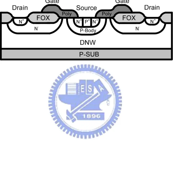
Silicon laterally diffused metal oxide semiconductor (LDMOS) transistors have been of great interest due to their applications in RF amplifiers in wireless communication systems or base-stations [24]. LDMOS transistors provide several advantages, including high efficiency, low cost and good linearity capability on silicon substrates. Scaling down the gate length or the drift length of LDMOS transistors improves their performance by producing lower on-resistance and higher transconductance. However these scaling approaches may limit high-voltage endurance during power-amplifying operations.
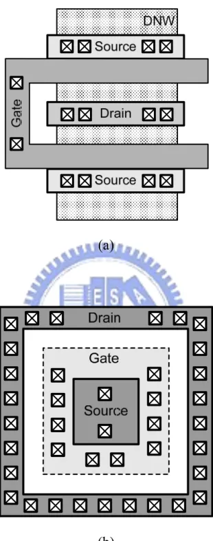
In addition to scaling down the device or changing device processes, researchers have studied several transistor layout styles in their search for the best device performance [25]. These designs must deal with the tradeoff between layout area and reduced parasitic. The results presented in this study show that closed transistors offer many promising characteristics. The most widely used closed topology is the square-structure transistor as shown in Fig. 2.1. The square-structure transistor has lower on-resistance and higher transconductance, as described in [26]. However, square-structure corners contribute very
applied voltage is high with respect to the channel length, the electric field in the corners could break the device. In this case, a circle-type layout, called an annular structure in this paper, would be the optimum layout type for ensuring the most uniform current flow. However, some works are only published in a square shape or polygonal shape due to foundry process restrictions [28][29]. Besides, this study also performs the capacitance analysis. Due to the capacitance influence of the input and output of enclosed devices, which are significant in dynamic operation and have an impact on device high-frequency performance, many studies have been published on the capacitance characterization and modeling of LDMOS transistors [30-32].
2.2 Annular-structure RF LDMOS
2.2.1 Device Design and Fabrication
In this study, fabricates the annular-structure RF LDMOS transistors were fabricated using a 0.5 μm LDMOS process. The standard LDMOS layout consists of a source and a drain separated by a channel of width W and length L. An annular-structure LDMOS consists of a transistor with the source diffusion in the middle, encircled by the gate channel and the drain diffusion to achieve a lower ON-resistance [33]. The channel width for annular structure is the length of the curve lying at mid-channel.
Figures 2.2 and 2.3 show the die photo and single cell layout of an annular-structure LDMOS transistor. Figure 2.4 illustrates the schematic cross section of this device. The gate oxide thickness was 135 Å and the mask channel length (LCH,shown in Fig. 1.1) was 0.5 μm. The
drift length (LDrift=LOV+LFOX) was 2.4 μm. The drain region was extended under the field
oxide (FOX), consisting of a lightly doped N-well drift region and an N region with higher doses for on-resistance control. This design ties the source region and the p-body together to eliminate extra surface bond wires, reduce the source inductance, and improve the RF performance in a power amplifier [34]. This study optimizes the LDMOS transistor layout for high-frequency performance with a GSG structure adapted for on-wafer measurement.
2.2.2 DC Characteristics
Generally speaking, the DC characteristics of LDMOS are similar to the MOSFET. Nevertheless, at high drain voltages, the MOSFET suffers a breakdown caused by the high voltage across the oxide at the drain end of the gate, resulting in high gate-drain current flow. Another effect arising from the high electric field in this region is hot-carrier injection. However, in the LDMOS structures, these high-field effects are mitigated. The use of a lightly-doped n-type region at the drain end of the gate moves the heavily-doped drain contact region away from the high field region, and has a number of benefits. The lightly-doped semiconductor can support a high voltage, enabling the high RF voltage swing required for a
high-power device. The electric field in saturation at the drain edge of the gate is reduced, thereby reducing the hot-carrier injection and increasing the gate breakdown voltage [35].
The LDMOS transistor with larger LDrift revealed a lower drain current and
transconductance. Moreover, the breakdown voltage was higher with a larger LDrift device.
For a larger LDrift, the higher resistance in the drift region results in a large voltage drop which
increased the carrier velocity and go into the velocity saturation easily. The velocity saturation in the drift region is called “quasi-saturation” while intrinsic MOS is still in linear operation. This effect is generally observed at high gate voltages. When the device go into the quasi-saturation, the gate control ability decreases which limits the drain current level and delays the transition between linear and saturation region [36].
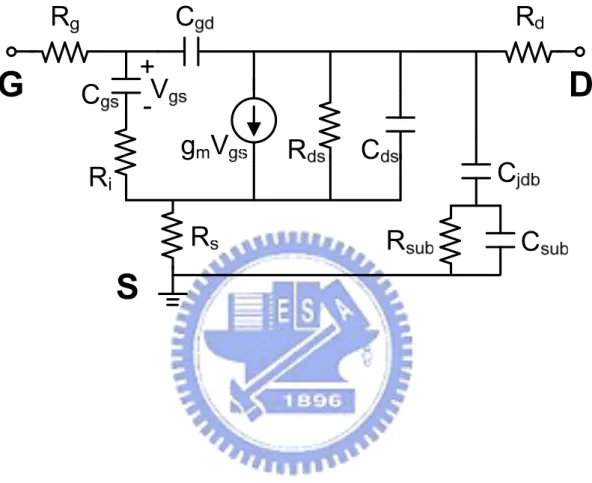
2.2.3 High-frequency Characteristics
Through small-signal equivalent circuit analysis of a MOSFET, we can realize the effect of device parameters on high-frequency characteristics easily. We adopted a simple equivalent circuit of the LDMOS by the method described in [37]. The equivalent circuit is shown in Fig. 2.5. After de-embedding the extrinsic parasitic resistances and the substrate-related parameters, the intrinsic components can be directly extracted from intrinsic Y-parameters by the following equations [38]:
)
Im(
1
12Y
C
gdω
−
=
(2.1))
)
)
(Im(
))
(Re(
1
(
)
Im(
2 11 2 11 11 gd gd gsC
Y
Y
C
Y
C
ω
ω
ω
−
+
⋅
−
=
(2.2))
Im(
1
12 22Y
Y
C
ds=
+
ω
(2.3) 2 11 2 11 11))
(Re(
)
)
(Im(
)
Re(
Y
C
Y
Y
R
gd i=
−
ω
+
(2.4))
Re(
1
22Y
R
ds=
(2.5))
1
(
)
)
)
(Im(
))
((Re(
2 2 2 2 21 2 21 0 gd gs i mY
Y
C
C
R
g
=
+
+
ω
⋅
+
ω
(2.6))
)
Re(
)
Im(
arcsin(
1
21 21 m i gs gdg
Y
R
C
Y
C
ω
ω
ω
τ
=
−
−
−
(2.7)The cutoff frequency (fT) can be expressed in
)
(
2
gs gd m Tg
C
C
f
=
π
+
(2.8)which is related to the intrinsic transconductance (gm) and input intrinsic capacitances (Cin =
Cgs + Cgd). The approximate maximum oscillation frequency (fmax) can be expressed as
)
(
8
4
maxf
Tg
DSR
gf
TC
gdR
gR
df
≈
+
π
+
α
(2.9)The drain-to-substrate junction capacitance (Cjdb) refers to the deep n-well (DNW) to
p-usbstrate/p-body junction capacitance and this capacitance also has impact on fmax.
2.3 Annular-structure and Square-structure Comparison
2.3.1 Effective Transconductance Evaluation
The initial problem in an annular-structure LDMOS is the definition of the aspect ratio W/L, which is not as complicated as in standard devices. However, defining the width (W) of the annular structure is less straightforward. For example, the width (W) can either the length of the curve lying at mid-channel, or the drain/source diffusion perimeter.
This study extracts the experimental W/L values by comparing the ID-VGS characteristics of
an annular-structure transistor and a standard transistor with the same L. The SPICE model can be used to extract W/L from the ratio of transconductances gm as follows [40]:
(
)
(1
)
D m eff ox DS DS GSI
W
g
C V
V
V
L
μ
λ
∂
=
=
+
∂
(2.10) closed std closed m std eff eff mg
W
W
L
L
g
⎛
⎞
=
⎛
⎞
⎜
⎟
⎜
⎟
⎝
⎠
⎝
⎠
(2.11)where the superscripts ‘std’ and ‘closed’ refer to the standard geometries and closed structure (square/annular structure), respectively. As the effective aspect ratio of the standard transistor that was called fishbone structure was known, the aspect ratio of the square/annular structure can be determined.
Figure 2.6 shows the I-V characteristics of a LDMOS under static conditions. The DC characterization of the DUT was performed using an Agilent semiconductor parameter (4156C) analyzer. In saturation region, the annular structure shows a higher drain current and transconductance than the square structure. These are attributable to the larger equivalent W/L and smaller drain parasitic resistance. The effective annular structure width is 83.2 μm compared with fishbone structure (W = 80 μm). These results show that the annular structure has better DC performance than the square structure.
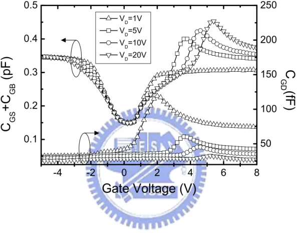
2.3.2 Capacitance versus V
GSand V
DSThis section extracts the gate-to-source/body capacitance (CGS + CGB) and gate-to-drain
(CGD) capacitance from the de-embedded S-parameters in the low-frequency range [41]. The
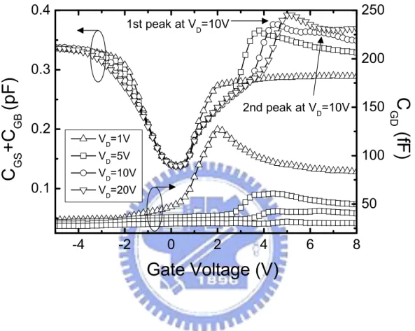
other capacitance extraction method was performed in the Appendix 1. Figures 2.7 and 2.8 show the extracted CGS + CGB and CGD of RF square-structure and annular-structure LDMOS
transistors at room temperature. At VDS = 1 V, both square and annular structures have similar
non-uniform doped channel in LDMOS, the drain end will be inverted prior to the source end, resulting in a peak in CGD. As the drain voltage VDS exceeds 5 V, the CGS + CGB and CGD all
start to reveal distinct peaks. This is because the inversion charges are injected to the depleted area of the drift. Therefore, the CGD and CGS + CGB increase with increasing VG, and the CGS +
CGB increases suddenly over the flat of the inversion area to reach the maximum at the onset
of quasi-saturation [36]. The reason for this phenomenon is that a higher VD leads to a higher
VG at the onset of quasi-saturation, and so the peaks shift to a higher VG.
However, for the square structure, Fig. 2.7 shows a second peak in CGS + CGB and CGD at
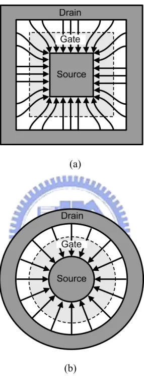
VDS = 10 V. Figure 2.9 shows a uniform current distribution across the region from drain to
source in annular structures. Because the corners of the drift of square structure show a lower current density than the edges, square-structure device must provide higher gate voltage to go into quasi-saturation. In other words, besides the first peak results from the edges of the square structure which went into the quasi-saturation region in advance, the second peak appears when the corners start to go into quasi-saturation at VG is approximately 6.5 V when
VDS = 10 V.
2.3.3 High-frequency Characteristics and Power Performance
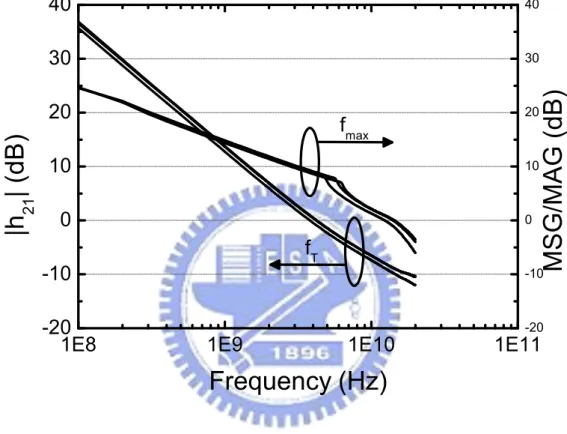
To characterize the high-frequency performance and determine the maximum cutoff frequency (fT) and maximum oscillation frequency (fmax) of annular-structure LDMOS
transistor, this study measures S-parameters on-wafer from 0.1 to 20 GHz using an Agilent performance network analyzer (E8361C) and then de-embeds them using the OPEN dummy [42]. The cutoff frequency and maximum oscillation frequency are the frequency where the current gain was 0 dB and the frequency where MSG was 0 dB, respectively. The measurement results of fT and fmax for annular-structure LDMOS are shown in Fig. 2.10. At
VG = 2 V and VD = 20 V, the cutoff frequency and maximum oscillation frequency are
approximately 5 GHz and 12 GHz, respectively.
This study measured power performance using a load-pull system consisting of HP85122A and ATN LP1 at the cascade probe station, with the probe calibrated using a standard calibration substrate. Figure 2.11 shows the transducer power gain and efficiency of different layout structures. In the case of the load-pull measurement, the operating frequency was 1.9 GHz and the source and load impedances were biased at VD = 20 V and VG = 2.5 V, which
are maximum cutoff frequency values. Figure 2.11 indicates a power gain of over 12 dB and an input power 7 dBm at the 1-dB compression point. The power added efficiency (PAE) at this point is over 20%. Figure 2.11 also shows that the annular structure had higher power gain and efficiency than the square structure. This result might be attributed to the larger equivalent transconductance of the annular structure.
2.4 Summary
Two types of layout structures of RF LDMOS transistors for DC, capacitance and power characteristics were investigated. The annular-structure LDMOS transistor had a better performance than the square structure without changing the process flow. The higher drain current in the annular structure LDMOS was due to less corner effect compared with square structure. According to the capacitance extraction results and power performances, the annular structure is superior to the square structure in layout type of LDMOS transistor.
(a)
(b)
0 5 10 15 20 25 30 0.0 5.0 10.0 15.0 20.0 25.0 30.0 VGS=1V VGS=2V VGS=3V VGS=4V Annular Square
Drain Current (mA)
Drain Voltage (V)
VGS=5V(a)
0 2 4 6 8 1E-9 1E-8 1E-7 1E-6 1E-5 1E-4 1E-3 0.01 0.1 VD=20V VD=1V Annular Square VD=20VGate Voltage (V)
Drain C
urrent (A)
VD=1V 0.0 2.0 4.0 6.0 8.0 10.0Transconductance (mA/V)
(b)
-4
-2
0
2
4
6
8
0.1
0.2
0.3
0.4
2nd peak at VD=10V VD=1V VD=5V VD=10V VD=20VGate Voltage (V)
C
GS+C
GB(pF)
1st peak at VD=10V50
100
150
200
250
C
GD(f
F)
Fig. 2.7 Extracted CGS+CGB and CGD versus gate voltage with different drain biases for
-4 -2 0 2 4 6 8 0.1 0.2 0.3 0.4 0.5 VD=1V VD=5V VD=10V VD=20V
Gate Voltage (V)
C
GS+C
GB(pF)
50 100 150 200 250C
GD(fF)
Fig. 2.8 Extracted CGS+CGB and CGD versus gate voltage with different drain biases for
(a)
(b)
Fig. 2.9 Schematic view of layout structure and current distribution in RF LDMOS. (a) square structure and (b) annular structure.
1E8
1E9
1E10
1E11
-20
-10
0
10
20
30
40
-20 -10 0 10 20 30 40f
TMSG/MAG (dB)
|h
21| (dB)
Frequency (Hz)
f
maxFig. 2.10 Cutoff frequency (fT) and maximum oscillation frequency (fmax) of annular-structure
-20
-15
-10
-5
0
5
10
-10
-5
0
5
10
15
20
Annular-structure Square-structurePin (dBm)
Ga
in
(d
B
), Po
u
t (d
B
m
)
0
5
10
15
20
PAE (%)
Fig. 2.11 Output power and efficiency versus input power at 1.9 GHz, VD = 20V, and VG =
Chapter 3
RF Transistor PHD Modeling
3.1 Introduction
Modern communication systems are nowadays complex to permit complete simulation of the nonlinear behavior at the active device level. In addition to small-signal and parasitic analysis for active devices, linearity and power analysis are the most important factors in RF amplifiers because it leads to intermodulation distortion. This type of distortion creates undesired signals, similar to the operation signal, in the amplifier input. In particular, the third order intermodulation distortion (IMD3) must be minimized because it generates harmonics that interfere with the desired signal. As a result, many studies have been dedicated to developing large-signal models to predict the nonlinear behavior of active devices [43-46]. Though these nonlinear models can predict the large signal operation of active devices accurately using suitable equivalent circuits or mathematical equations, they may be unsuccessful in other kinds of active devices or foundry processes. Optimizing circuit performance and reducing product time to market for accurate large-signal models remains an essential.
An alternate way to construct a large-signal model is to use the measurement-based behavioral method proposed by [47], called the polyharmonic distortion (PHD) model. This
model is based on X-parameters, which are extensions of S-parameters with nonlinear components measured using a nonlinear vector network analyzer (NVNA) [48]. S-parameters are perhaps the most successful parameter ever. These parameters have the powerful property that the S-parameters of individual components are sufficient to determine the S-parameters of any combination of those components [49]. S-parameters are sufficient to predict its response to any signal, provided only that the signal is small amplitude or power. Despite the great success of S-parameters, they have several limitations. The S-parameters are defined only for linear systems, passive component, or systems behaving linearly with respect to a small signal applied around a static operating point at active device. In fact, all systems are nonlinear in real world. Sometimes, they generate harmonics and intermodulation distortion. Therefore, the S-parameter analysis technique doesn’t apply to such systems. X-parameters include harmonic tone and intermodulation frequency component, and also the relationships between all those frequencies for given amplitude and frequency; therefore the X-parameters enable the engineer or system designer to acquire the complete spectrum or waveforms of nonlinear system [48]. Unlike S-parameters, the engineer could obtain the linear device behavior and nonlinear behavior about a large signal operation point from the X-parameters.
As discussed in a study [50], this measurement-based large-signal model facilitates amplifier design with RF simulation tool. Moreover, this study succeeds in calibrating the NVNA reference plane to probe tip. This study also presents the nonlinear behavior of RF
LDMOS transistors using the PHD model because the NVNA must calibrate the comb generator and power meter before large signal measurements.
3.2 Polyharmonic Distortion Model Theory
The waves of S-parameter are defined as linear combinations of the signal port voltage, V, and the signal port current, I, whereby the current quantity is defined as positive when traveling into the DUT. The incident and scattered wave are called the A-wave and the B-waves, respectively [49]. They are defined as follows:
2
0I
Z
V
A
=
+
(3.1)2
0I
Z
V
B
=
−
(3.2)The value of the characteristic impedance Z0 is 50 Ω. This analysis aimed at PHD model will
be working with nonlinear functional relationships between the wave quantities. This derived process of PHD model is very different from S-parameters that can only describe a linear relationship. The PHD model assumes that the discrete tone signals appeared on the incident as well as for the scattered waves. Furthermore, these discrete tones may appear at arbitrary frequency, as explained in [48]. For a given active device, determine the set of complex functions Fpm(.) that correlate all of the relevant input components Aqn with the output
components Bpm, where q and p are from one to the number of signal ports, and m and n are
from zero to the highest harmonic index. The mathematical equation expressed as
,...)
,
...,
,
(
A
11A
12A
21A
22F
B
pm=
pm (3.3)Note that the complex functions Fpm(.) are called the describing functions [51]. This
mathematical equation is illustrated in Fig. 3.1. The spectral mapping (3.3) is a very general mathematical form; therefore the practical models can be developed in the frequency domain from this form. The PHD model is a special approximation of (3.3), which involves the linearization of (3.3) around the incident or scattered signal.
A first property is that Fpm(.) describes a time-invariant system. This implies that applying
an arbitrary delay to the input signals, the incident A-wave, always results in exactly the same time delay for the output signals, the scattered B-waves. In the frequency domain, applying a time delay is equivalent to add a linear phase shift (θ). Therefore, the complex function equation (3.3) can be expressed as
,...)
,
,...,
,
(
:
2 22 21 2 12 11 θ θ θ θ θθ
j j j j pm jm pme
F
A
e
A
e
A
e
A
e
B
=
×
∀
(3.4)model equations. Because the (3.4) is valid for all values of θ, we can make equal to the inverted phase of A11 which is the incident fundamental. The choice is not unnatural for
power transistor and power amplifier applications, since A11 is the dominant large-signal
input component.
For expression elegance, the phasor P is introduced and is defined as
) (A11 j
e
P
=
+ ϕ (3.5) Substituting ejθ by P-1 in (3.4) results in m pm pmF
A
A
P
A
P
A
P
A
P
P
B
=
(
,
−,
−,...,
×
−,
−2,...)
+ 22 1 21 3 13 2 12 11 (3.6)The benefit of (3.6), compared to (3.3), is that the first input argument will always be a positive real number, that is to say, the amplitude of the fundamental component at the input port 1, instead a complex number.
The harmonic superposition principle is illustrated in Fig. 3.2. To keep the diagram simple and elegance, this PHD model derived thereafter only consider the presence of the A1m and
B2n components and neglect the presence of the A2m and B2n components. The harmonic
all components in this equation besides the large signal A11 results in
)
Im(
)
(
)
Re(
)
(
)
11
(
11 , 11 , n qn m qn pg mn n qn m qn mn pg m pmP
A
P
A
H
P
A
P
A
G
P
A
Kpm
B
− + − + +∑
∑
+
+
=
(3.7) whereby 0 ,... 0 , 11 , 0 ,... 0 , 11 , 11 11 11 11)
Im(
)
(
)
Re(
)
(
),
0
,...
0
,
(
)
(
A n qn pm mn pq A n qn pm mn pq pm pmP
A
F
A
H
P
A
F
A
G
A
F
A
K
− −∂
∂
=
∂
∂
=
=
Note that the real and imaginary parts of the input arguments are considered as separate and independent parts. The PHD model equation is derived by substituting the real and imaginary parts of the input arguments in (3.7) by a linear combination of the input arguments and their corresponding conjugates. Since
2
)
(
)
Re(
n qn n qn n qnP
A
conj
P
A
P
A
− − −=
+
(3.8)j
P
A
conj
P
A
P
A
n qn n qn n qn2
)
(
)
Im(
− − −=
−
(3.9)⎟
⎟
⎠
⎞
⎜
⎜
⎝
⎛
−
×
+
⎟
⎟
⎠
⎞
⎜
⎜
⎝
⎛
+
×
+
=
− − + − − + +∑
∑
j
P
A
conj
P
A
P
A
H
P
A
conj
P
A
P
A
G
P
A
Kpm
B
n qn n qn m qn mn pg n qn n qn m qn pgmn m pm2
)
(
)
(
2
)
(
)
(
)
11
(
11 , 11 , (3.10)Rearranging (3.10), and then the simple PHD model equation as follows
)
(
)
(
)
(
11 , 11 , qn n m qn pqmn qn n m qn pqmn pmS
A
P
A
T
A
P
conj
A
B
=
∑
+ −+
∑
+ + (3.11)The Spq,mn(.) and Tpq,mn(.) are defined as
,
)
(
)
(
11 11 11 1 , 1A
A
K
A
S
p m=
pm (3.12)0
)
(
11 1 , 1A
=
T
p m (3.13){ } { }
2
)
(
)
(
)
(
:
1
,
1
,
, 11 , 11 11 ,A
jH
A
G
A
S
n
q
pgmn pqmn mn pq−
=
≠
∀
(3.14){ } { }
2
)
(
)
(
)
(
:
1
,
1
,
n
T
,A
11G
,A
11jH
,A
11q
≠
pqmn=
pg mn+
pqmn∀
(3.15)optimization, the PHD model is a good way to analyze the nonlinear characteristics for active devices. The X-parameter in Agilent nonlinear vector network analyzer expression is given by (3.16). QL L K L Q S QL PK K F PK PK
X
A
G
X
A
G
A
B
=
+
∑
−⋅
, 11 ) ( , 11 ) ((
)
(
)
∗ +⋅
+
∑
K L QL L Q T QL PKA
G
A
X
, 11 ) ( ,(
)
(3.16)Here the scattered and transmitted waves, BPK, at port P at the Kth harmonic frequency,
divided into three terms. The first term represents the large-signal response of the device to a single large-amplitude tone (A11) at a given fundamental frequency, assuming match all ports
at all harmonic frequencies. The second and third terms depict a linear non-analytic mapping of incident phasors at port Q and harmonic frequency index L into complex output phasors at port index P and harmonic frequency index K. The term G is the phase of the input large tone. The sum of this equation includes all ports and indicates the number of harmonics measured. The significance of expression (3.16) is the same with (3.11), and the (3.16) is read easily for reader. Consequently, the X-parameters in the PHD model are mathematically generalized
S-parameters, applicable to nonlinear and linear components under both large-signal and small-signal conditions.
3.3 RF Active Device Power Characteristics
3.3.1 Measurement Setup and On-wafer Calibration
This study used an Agilent Nonlinear Vector Network Analyzer (NVNA) capable of nonlinear calibration and measurements to extract the PHD model. Figure 3.3 illustrates this nonlinear measurement system. The system is based on a dual-source network analyzer (PNA-X) with two phase reference comb generators for phase calibration and a power meter and sensor for power calibration. This system also includes embedded application software and an interface for other instruments to automatically control X-parameter characterization and extraction. Using standard nonlinear analysis tool in Agilent Design System (ADS), the measured DUT X-parameters can be immediately used to simulate nonlinear figures of merit such as P1dB, IP3, time waveform and other power performance. Therefore, the on-wafer
calibration of this system is very important to accurately acquiring the simulation results of active devices. The S-parameters of the GSG probes were measured before system calibration. This is because the NVNA phase and power calibration are just for the cable end, and not for the probe tips (Fig. 3.3 depicts the calibration reference plane). When finished the S-parameters, phase, and power calibration at cable end of the NVNA system with phase
stable coaxial cable, add up the S-parameters of probes to NVNA system; therefore, the calibration plane will shift to the probe tips. Figure 3.4 shows the actual hardware setup of NVNA system.
3.3.2 Linearity and Power Performance
The PHD model results agree well with the nonlinear behavior of the annular/square-structure LDMOS transistor with 80 μm width length at 1.9 GHz. The impedance of measurements results and extracted data are all at 50 ohm. Figure 3.5 and 3.6 show that the PHD model accurately predicts the measured transducer power gain and the third-order intermodulation (IM3) over a wide range of input power. Figure 3.7 represents a comparison between the measured and modeled (by means of the PHD model) time domain voltage waveforms at the terminals of the annular-structure RF LDMOS. Figures 3.8 and 3.9 measure gain contours by ATN LP1 and simulate the other using the ADS simulator. The simulating transducer gain contours for 80 μm width length in the annular structure agree with measurement data even at the maximum value far from the 50 ohm.
3.4 Summary
The nonlinear behavior of an annular structure LDMOS transistors using PHD model presented in this study. By way of the on-wafer NVNA measurement system, the nonlinear model via X-parameter provides a simple and direct way to get a large-signal model for power amplifier design. The linearity and power gain contour can be predicted using this model without any optimization and curve fitting.
A
1mB
1kA
2mB
2k,...)
,
...,
,
(
11 12 21 22 1 1F
A
A
A
A
B
k=
k,...)
,
...,
,
(
11 12 21 22 2 2F
A
A
A
A
B
k=
k-20
-15
-10
-5
0
5
10
15
-8
-7
-6
-5
-4
-3
-2
Gain (dB)
Pin (dBm)
Annular Measured Annular Simulated Square Measured Square SimulatedFig 3.5 Measured and simulated results of the gain for annular-structure and square-structure LDMOS transistors with width 80 μm at 1.9 GHz.
-15
-10
-5
0
5
10
-100
-80
-60
-40
-20
0
Measured SimulatedPout
and I
M
3 (dBm)
Pin (dBm)
Fig. 3.6 Measured and simulated results of the IM distortion for annular-structure LDMOS transistors with total width length 80 μm at 1.9 GHz.
0 200 400 600 800 1000 -6 -4 -2 0 2 4 6 B2 Wave Simulation
Volts (V)
Time (ps)
(a)
(b)
Fig. 3.8 Measured results of gain circle for annular-structure LDMOS transistors from load-pull system with total width length 80 μm at 1.9 GHz.
0.2 0.5 1.0 2.0 5.0 -0.2 0.2 -0.5 0.5 -1.0 1.0 -2.0 2.0 -5.0 5.0
Fig. 3.9 Simulated results of gain circle for annular-structure LDMOS transistors from PHD model with total width length 80 μm at 1.9 GHz.
Chapter 4
Sensing Application
4.1 Introduction
The commercial market has rapidly grown for demanding various sensitive sensors in areas including chemistry, medicine and biology. Although surface acoustic wave (SAW) filters have seen much use in telecommunication, SAW-based sensors have recently emerged for many attractive features in medical and chemical applications [52][53]. The use of acoustic microsensor to detect the physical properties, such as mass loading and viscosity, provides the benefits of real-time electronic readout, compact size, robustness, and low cost. Monolithic integration of biosensors with existing microelectronics will allow biochemical detection system to be further miniaturized in mass production and enhanced with software-definable functions. Chemical sensing through the use of acoustic wave devices has long been available using ST-quartz as the piezoelectric material for generating acoustic wave. Vapor and gas sensors based on SAW oscillators have been progressing since Wohltjen reported the first studies in 1979 due to their high sensitivity and low production cost [54]. A SAW chemical or biological sensor is commonly realized by a polymer-coated delay-line resonator as the frequency control element in the feedback loop of an oscillating circuit.
Relative to sensing applications, using monolithic integration technology, have been demonstrated [55-58]. These studies developed to date only have a sensor system without any sensing experiments. Although these studies have developed a sensor system using silicon or GaAs process, these sensing performances lack some experiments to show its feasibility. Therefore, in order to modulize and miniaturize the sensing system, it is of great interest to develop chemosensor or biosensor systems by taking advantages of matured IC processing technologies and validate the sensor with sensing experiment in this research.
In this work, the fabrication of SAW devices and the related oscillating circuit using two-poly two-metal (2P2M) 0.35 um complementary metal-oxide-semiconductor (CMOS) process are investigated. Their electrical characteristics are evaluated as well as vapor sensing results. The SAW sensor with the CMOS circuitry is a potential candidate for the development of highly sensitive and low power microsensors.
4.2 Basic Sensing Mechanism
Although the acoustic wave detects any change of the mechanical or electrical boundary conditions on the piezoelectric substrate surface, it is mainly the mass loading effect that is used in chemical sensors. In this case, an appropriate measure for sensing is the fractional frequency shift Δf/f0 caused by a change in the mass loaded onto the surface, where f0 is the
operation frequency of oscillator without vapor adsorption. This fractional frequency shift can be given by [59] 0 0
f
Cf h
f
ρ
Δ
=
Δ
(4.1)where C is a frequency-independent constant, h denotes the thickness of the coating film that incorporates vapor molecules, and Δρ is the mass density change due to absorption.
The phase noise measurement is a typical way to determine whether the signal of oscillator that was designed as sensor is stable or not. High signal stability in the oscillator is important for differentiating sensing result. Phase noise is defined to quantify the fluctuations of signal in frequency domain, and expressed as the ratio of the single side-band power at a frequency offset Δω from the carrier with a measurement bandwidth of 1 Hz to the carrier power. The phase noise can be theoretically expressed in the following equation:
{ }
⎥
⎥
⎦
⎤
⎢
⎢
⎣
⎡
⎟
⎟
⎠
⎞
⎜
⎜
⎝
⎛
Δ
Δ
+
⎟⎟
⎠
⎞
⎜⎜
⎝
⎛
Δ
+
=
Δ
ω
ω
ω
ω
ω
1 3 2 01
2
1
2
log
10
f carrierQ
P
FkT
L
(4.2)ω0 is the oscillation frequency, Δω is the offset frequency from the oscillation frequency and
Δω1/ f 3 is the corner offset frequency between the 1/ f 3 and the 1/ f 2 regions in the phase noise
response. Equation (4.2) is simplified considerably in our case because SAW devices have an exceptional performance regarding flicker noise (1/f noise) [61]. Only if the amplifier is the dominant noise source will an increase in Q result in reduced oscillator flicker noise. Base on (4.2), improving the Quality factor of SAW device and increasing the power of oscillator appropriately will lower the phase noise to obtain an ideal oscillator for sensing purposes.
4.3 Circuit Design and Experiments
4.3.1 Device Design and Fabrication
A SAW Device having inter-digital transducers (IDT) on the quartz substrate in this study is a key component in the sensing circuit. When an electrical signal of a certain frequency is applied to the input IDT, the SAW is excited on the surface of the substrate because of its piezoelectric effect, and then the SAW propagates across the surface of the substrate toward the output IDT. Figure 4.1 shows the schematic layout of a two-port SAW device in this work. Two single-finger interdigitated transducers were fabricated on an ST-quartz substrate with a propagation direction perpendicular to the x-axis of the quartz. The electrodes were 1/4 wavelength wide and separated by 1/4 wavelength at the target center frequency. A predetermined 157 MHz SAW device whose λ is approximately 20 μm was then designed
with a delay path length of 10λ, and IDT length of 100λ, and uniform aperture width of 70 [62]. A wire-bonded SAW device in the metal can package is shown in Fig. 4.2(a). The SAW device with a metal cap is used to prevent gas disturbance from the ambient as shown in Fig. 4.2(b).
Early reported sensing experiments were conducted to measure the center frequency shift or phase shift of a SAW device using the vector network analyzer (VNA) to directly monitor the frequency response on the SAW device [63]. However, these sensing results by reading the VNA have shown less sensitivity and complicated VNA calibration in gas sensing. In this study, a CMOS-based oscillating circuit for a vapor sensor was accomplished. Before full circuit implementation, a summary of circuit design scheme is presented in Fig. 4.3. For an oscillator to be used in biochemical detection, a MOS amplifier with a feedback loop through the SAW delay line is designed. In order to meet Barkhausen criteria, the amplifier must provide sufficient gain at the target oscillator frequency to overcome the SAW insertion loss as well as the phase difference. Thus the oscillator successfully oscillates as long as the following conditions are satisfied:
1 2 1 2
(
)
(
) 0
a B B s M M
G
+
G
+
G
+
L
+
L
+
L
≥
(4.3)In the above equations, Ga, GB1, and GB2 are the gain of the amplifier and buffer amplifiers as
shown in Fig. 4.3; LS, LM1,and LM2 are the losses of the saw device and match circuits
respectively; φa, φB1,and φB2 are the phases of the amplifier and buffer amplifiers; φs, φM1,and
φM2 are the phases of the saw device and match circuits respectively. As changes occur due to
mass loading or temperature, the oscillating frequency will change to maintain a multiple of 360° phase shifts in the oscillator loop. In the amplifier design, the enhancement load amplifier is chosen to avoid resistors. Therefore, the lowest phase noise will be achieved easily. Furthermore, the cascade buffer amplifier improves the isolation between input and output of an enhancement load amplifier. Thus an improved stable and stable gain will be obtained. Figure 4.4 illustrates the schematic of CMOS amplifier circuits and measurement result. The open-loop gain of the amplifier is above 20 dB at 157 MHz in Fig. 4.4(b).
The flow to accomplish a SAW sensing circuit is shown in Fig. 4.5. There are three major parts in the SAW sensing system including a SAW delay line sensor, a CMOS amplifier and matching networks. First, the SAW device has been designed and fabricated based on the required electrical properties as discussed in the previous section. After completing the SAW device, an amplifier was designed and tuned based on the center frequency and insertion loss of the SAW device. Next, the circuits of phase matching should be considered to compensate the SAW device and CMOS amplifier. For various sensing experiments and conditions, additional passive components were needed to achieve proper phase matching. While the chip
process was completed, the SAW device was wire-bonded with the amplifier in a PCB or metal-can package. The SAW delay line and amplifier were initially characterized by a network analyzer, respectively. A picture of the processed CMOS chip (1.3 x 1.3 mm2) is shown in Fig. 4.6.
4.3.2 Sensing System
Sensing systems with closed chambers were proposed in some studies [63]. The chemical sensor was reported to successfully detect ethanol in previous literature [64][65]. Figure 4.7 shows the schematic of a simple sensing system in this study. The SAW device was hermetically sealed in the metal can package, as indicated in Fig. 4.2(b) to minimize the residual gas volume and reduce the reaction time. Alcohol vapor was diluted by dry nitrogen and flowed into the metal can package when the flow control valve in this system was turned on. Furthermore, the alcohol concentration was detected by infrared spectrophotometer (IR) system. When the valve was turned off, only pure dry nitrogen flowed into the metal can package. The gas flow rate was 100 sccm. All measured data, including those of the frequency shift, were acquired by data acquisition modules (DAQ), and then analyzed by a personal computer (PC).
4.4 Results and Discussion
In order to acquire the repeatable sensing results, it is important to analyze the quality of signal by phase noise measurement. The SAW oscillator was tested with a commercial spectrum analyzer with Vd = 3 V. The phase noise of the oscillator was measured by Agilent
E5052A signal source analyzer. The operating frequency of the oscillator is 157.2 MHz as shown in Fig. 4.8. The phase noise of this oscillator is shown in Fig. 4.9. The achieved phase noise of the oscillator with SAW device is –150 dBc/Hz at 100 kHz offset. Comparing to the traditional oscillator design with inductance-capacitance (LC) tank, the oscillator with SAW device in this study has well phase noise value at 100 kHz due to the high-Q in SAW devices [66]. The excellent phase noise would stabilize the peak frequency drift in the oscillator. The power consumption was 70 mW and expected to be reduced if the SAW device is properly matched in its impedance and the RF amplifier is further optimized. A lower insertion loss in the SAW would be desirable for a low gain amplifier. In this work, the insertion loss of SAW device was about –20 dB.
After completing the SAW oscillator, the SAW device was tested in a gas sensing system. The sensor was exposed to 50 x 103 ppm of alcohol. A 600-s exposure time was used for each alcohol pulse. The alcohol sensing results by a thin polyepichlorohydrin (PECH) polymer film on a SAW device are demonstrated in Fig. 4.10. The alcohol molecules are absorbed into the PECH film on the SAW device. As alcohol molecules gradually diffuse into the PECH
film, the SAW oscillating frequency shifts because of mass loading effect. Consequently, the maximum oscillation frequency shift between gas on and off is approximately 10 kHz.
4.5 Summary
In this chapter, the monolithic integration of a SAW delay-line sensor and a 0.35 μm CMOS amplifier has been demonstrated for the organic vapor sensing application. The circuit scheme and design flow of the oscillator with a SAW device are also presented in this study. The gain and total power consumption of the amplifier are 20 dB and 70 mW, respectively. The phase noise of the SAW oscillator achieves –150 dBc/Hz at 100 kHz offset. The sensing experimental results show that the maximum oscillation frequency shift between gas on and off is approximately 10 kHz with 50 x 103 ppm alcohol vapor concentration. This compact integrated microsensor will be promising for future chemical and biological sensing applications.