國
立
交
通
大
學
電子工程學系 電子研究所
博 士 論 文
電阻式記憶體之特性研究及電性探討
The investigation on electrical characteristics and switching properties of
resistive random access memory
研 究 生:曾文賢
指導教授:張國明 教授
劉國辰 教授
電阻式記憶體之特性研究及電性探討
The investigation on electrical characteristics and switching properties of
resistive random access memory
研 究 生:曾文賢 Student:Wen-Hsien Tzeng
指導教授:張國明 Advisor:Kow-Ming Chang
劉國辰
Kou-Chen Liu
國 立 交 通 大 學
電子工程學系 電子研究所
博 士 論 文
A DissertationSubmitted to Department of Electronics Engineering and Institute of Electronics
College of Electrical and Computer Engineering National Chiao Tung University
in partial Fulfillment of the Requirements for the Degree of
Doctor of Philosophy in
Electronics Engineering May 2011
Hsinchu, Taiwan, Republic of China
電阻式記憶體之特性研究及電性探討
學生:曾文賢
指導教授:張國明
劉國辰
國立交通大學
電子工程學系 電子研究所
摘 要
隨著可攜式電子元件的蓬勃發展,如手機及數位相機,非揮發性記憶元件在半導體產 業的需求也日益增加。現今主流的非揮發性記憶元件為快閃式記憶體,然而快閃式記憶體 存在一些必頇克服的問題,如操作電壓較高、操作速度較慢以及記憶力隨元件尺寸微縮而 降低等。因此新興的非揮發性記憶體也逐漸受到重視。在這之中,以電阻式記憶體(RRAM) 最被看好。電阻轉換記憶元件具有操作電壓低、功率消耗低、操作速度快、可微縮性高、 記憶時間長、耐久力佳及尺寸小、易和半導體製程匹配等優勢。RRAM 是透過外加電壓或電 流將氧化層決定至高或低阻值,以用以作為分辨 0 或 1 不同阻態之記憶體應用。然而,至 今主要的轉態機制又依材料特性而異,而且影響 RRAM 的電性表現的效應至今依然有著探討 的空間。 在此論文中,分別以二氧化鉿、三氧化二釓和鋁酸鑭材料來作為氧化層,並探討其在 不同效應下的電性表現行為。這三種高介電材料是近年來閘極氧化層應用的候選材料。因 此若能有良好的電阻轉態特性,則有利於 1T1R 在製程上的整合製作。探討的參數變因包含 了本質的調變和外質的調變。本質調變參數有:上電極材料(鉑、鈀、鎳、鈦、鉭、鋁、 鎢、鋁、氮化鈦)、操作模式(電壓驅動和或電流驅動)、操作極性(單極操作和雙極操 作)、電極製程條件(電子束蒸鍍和濺鍍沉積)、沉積氧分壓條件、沉積溫度條件。而外 質調變參數有:氮環境熱處理、氮氧環境中熱處理、紫外光效應。無論是單極操作或雙極 操作的電性轉態行為,我們均提出可能的物理模型架構來解釋轉態機制,並且我們也能在
電性表現上有所提升和改善。 研究結果顯示,我們上述幾項研究變因參數皆會對轉態特性的好壞有所影響,而且氧 化層和上電極之間的介面對於轉態特性的好壞扮演著極為重要的角色。選取適當的製程方 式和製程參數,再搭配適合的上電極,我們能大幅提升單極操作的二氧化鉿的轉態特性。 而當我們對介面進行處理,如照紫外光、以氟化氫溶液蝕刻表面、熱處理,皆得到相對較 差的特性。我們的可逆實驗更加證實了介面的好壞可由我們人為的影響,來決定最後單極 轉態電性的操作穩定性。在不同上電極材料的研究中,我們曉得二氧化鉿單極操作的特性 是和上電極材料有關,更深入的研究,發現是上電極和氧化層之間所形成的中間層在主導 著轉態電性的好壞。普遍接受的單極操作機制是,在 ON 操作時施加正偏壓將氧化層裂化, 大量的氧離子被粹取至上電極介面。而 OFF 操作時,大量電流流過細小的細絲傳導路徑, 產生高溫的焦耳熱,而因造成細絲路徑斷開,而回到高電阻態。因此,我們選取能提升二 氧化鉿材料熱穩定性的材料鋁來作適當的添加,當二氧化鉿的熱穩定性被提升時,的確能 有效的提升其在單極操作時的耐久度。在不同的熱處理和氧處理下,當介面的缺陷更加的 被修復時,而造成細絲路徑的聚積,只是部份幾條細絲做傳導,因此在 ON/OFF 之間的切換 更加的好控制,因此電壓散佈度也能有效的控制。而當氧化層表面受紫外光照射,或是電 漿離子轟擊時,會造成氧化層表面的缺陷數量增加,如此會造成細絲路徑更加的散亂和任 意的形成,因此會得到相對較差的轉態特性。 在雙極操作方面,我們也進行了研究。雙極特性的穩定與否,電極材料亦扮演著關鍵 角色。正開負關或是負開正關的電阻轉態特性及其特性的穩定度,決定於介面層形成的好 壞。我們以脈衝雷射沉積法(PLD),來探討不同沉積溫度和氧分壓環境下所沉積的氧化層薄 膜,其對於轉態特性的影響。研究成果顯示,在高溫下沉積的薄膜,其結晶性較好,表面 的粗糙度變差,而在下電極和氧化層之間會有中介層形成。這層中介層也提供了氧的儲存 槽的作用,以供氧離子能作來回的移動,因此會有較佳的電阻轉態的特性。施加負偏壓, 將氧離子驅入至儲存槽中,因而路徑形成,轉態至 ON 態,施加正偏壓,將氧離子拉回氧化 層中,因此路徑被修復斷開,轉態至 OFF 態。而在氧分壓高的環境中沉積,過多的氧原子 會在沉積過程中反覆的和濺擊出來的沉積原子反應和碰撞,長成的薄膜結構較為緻密,可 長成非晶態的鋁酸鑭氧化層。在氧分壓大中的環境沉積,能得到較粗糙的表面,薄膜和氧 也鍵結愈強,表示氧空缺的量會大幅降低。而氧分壓大沉積過程易有碰撞,有些氧離子會 被撞擊至詴片表面,愈易造成中介層的生成。電性表現方面,在氧分壓大中沉積者有較大 崩潰電壓、較低漏電流、較穩定的轉態特性及較佳的操作電壓散佈度。從電性傳導的角度,
來回推適合穩定 RRAM 操作的電性傳導應該為何。值得提出的一點是,我們亦成功的製作出 透明的電阻式記憶體,克服了 ITO 電極不適合作為電極操作的問題。並擴展電阻式記憶體 的可利用範圍。
The investigation on electrical characteristics and switching
properties of resistive random access memory
Student:Wen-Hsien Tzeng
Advisors:Kow-Ming Chang
Kou-Chen Liu
Department of Electronics Engineering and Institute of Electronics
Nation Chiao Tung University
Abstract
Due to the popularity of portable equipment, such as mobile phone and MP3 player, the requirements of nonvolatile memory (NVM) increase significantly in the semiconductor industry. Flash memory is the mainstream among the nonvolatile memory devices nowadays, but several bottlenecks emerge, such as high operation voltage, low operation speed, poor endurance, and the scaling problem. The device dimensions are continuously scaled down, the flash memory faces the challenge of thin tunneling oxide that causes an unsatisfactory retention time. Therefore, the novel NVMs attract much attention in recent years. One of the promising candidates of next-generation NVMs is the resistive random access memory (RRAM) owing to its low operation voltage and power, high operation speed, high scalability, good endurance, small size, etc. However, the RRAM devices still exist many issues needed to be improved before the commercial application.
In this thesis, we investigated the electrical characteristics by using HfOx, Gd2O3, and
LaAlO3 as the insulator layer. The three kinds of high-k dielectrics are the candidates that have
been identified by the semiconductor industry as a potential replacement for SiO2 in gate
dielectric layers. Once these materials can exhibit reliable resistive switching properties, it can be a good choice for 1T1R integration application. The varying parameters we focus on including the intrinsic modulation (about metal-insulator-metal itself) and extrinsic modulation (post treatment). The intrinsic modulated parameters, such as top electrode material (Pt, Pd, Ni, Ti, Ta, Al, W, Cu, and TiN were used, respectively), operation mode (voltage bias operation or current bias operation), operation polarity (unipolar switching or bipolar switching), electrode
fabrication process (E-Gun deposition or sputtering deposition), oxygen partial pressure condition and deposition temperature and the extrinsic modulated parameters, such as thermal treatment in N2, thermal treatment in N2/O2, UV light exposure effect, etc., were all discussed.
For the unipolar and bipolar resistive switching characteristics, we both proposed the possible model to explain the switching mechanism. In addition, we can improve the electrical properties by modulating the above treatment.
The results reveal that the switching characteristics can be influenced by the modulated parameters listed above. In the investigation on electrical properties of HfOx films by using
different metal materials as top electrode, we observed that the unipolar switching characteristics are highly correlated to the top electrode materials. We further found that the interfacial layer formed between electrode and insulator film during deposition greatly dominates the switching properties. Based on the proposed unipolar switching mechanism, the general accepted model is the formation and rupture of the conducting filamentary paths, which is driven by the field for SET (OFF to ON) operation and thermal effect for RESET (ON to OFF) operation. We tried to improve the thermal instability of HfOx by adding Al thin layer at the top insulator surface. Once
the thermal stability of HfOx was improved, higher thermal stability of HfAlO layer can
effectively prevent the thermal noise against the unintentional stimulus, so the switching characteristics will be much better than that of other samples. In the study on post treatment, when samples are treated by oxygen gas at high temperature, defects at the surface will be oxidized and reduced. This can effectively confine the conducting filamentary paths to some local weak point, thus the random distribution of the conducting filamentary paths inside the insulator films can be avoided. The high and low resistance values can be greatly improved under the certain conditions of oxygen gas treatment. When samples surface were exposed under UV light (wavelength and laser intensity is about 365 nm and 80 mW/cm2) or plasma ions bombardment, defect density at the insulator surface will be increased. Once the defect density increases, the filamentary paths tend to form in a random connection under the applied bias, so a much poor switching properties would be expected. We can modulate the defect density at the insulator surface by the depicted experiments above to control the resistive switching characteristics.
In bipolar operation, the electrode material also plays an important role to the bipolar switching properties. We also observed that the operation polarity depends on the interfacial layer. We investigated the process condition effect to the switching properties based on by pulsed laser deposition. Different process condition, such as deposition temperature and oxygen partial pressure, were experimented and discussed. The results reveal that when thin films
deposited at higher temperature, it has better crystallinity, larger surface roughness, and a thicker interfacial layer formed at the bottom electrode and insulator interface. The higher crystallinity can provide more grain boundaries inside the insulator films, which facilitate the migration of the movable oxygen ions. The interfacial layer can serve as a good oxygen reservoir for the oxygen ions rested under the negative bias. So, the state can be switched to ON state. When the positive bias was applied, the oxygen ions back to oxidize with the metallic defects inside insulator films, so the state was switched to OFF state. We also discuss the amorphous insulator films as the application for RRAM devices on LaAlO3 thin films grown under different oxygen partial
pressure. We clearly explain how different oxygen partial pressure influences the surface roughness, the formation of the interfacial layer, the leakage current density, the forming voltage and the transparent resistive switching characteristics of the LaAlO3 thin films. The
micro-structure and oxygen concentration different inside LAO thin films may be the main reason for the distinction of the electrical characteristics, as well as the resistive switching properties. LAO films grown at higher oxygen partial pressure is beneficial for a more reliable resistive switching performance, because the formation of the interfacial layer and lower oxygen vacancy concentration exist in the LAO thin film. Migration of the oxygen ions between the interfacial layer and the LAO films under applied bias may be the possible switching mechanism. We successfully fabricated the transparent RRAM (T-RRAM) based on Gd2O3 and LaAlO3 thin
films on glass substrate and extended the application of RRAM to the transparent electronics filed.
誌
謝
首先我要感謝我的指導教授張國明教授,我才能順利的完成此博士論文。不 論是在學術研究與待人處世上,都給予許多的指導與幫助。另外,我要感謝另一 位指導教授長庚大學光電所劉國辰教授,在老師多年來耐心的教導之下,學到了 許多實驗的研究方法,遇到問題學會去思考並且尋求解決之道,以及待人處世應 有的腳踏實地與務實的態度,讓我博士班生涯受益良多。 感謝汪大暉教授、吳建宏教授、林鴻志教授、曾俊元教授、傅昭銘教授、趙 天生教授及蔡銘進組長,於百忙之中撥空擔任我的論文口詴委員,並對本論文提 出許多寶貴的意見,使其更臻完善。 再來要感謝在這段研究生涯中,實驗室學長同學與學弟們的幫忙。感謝王敬 業學長、賴瓊惠學姐、林稔杰學長、趙高毅學長、林俊銘學長、郭俊銘學長、林 建宏學長、張知天學長、黃士軒學長、陳柏寧學長、陳巨峰學長等人的指導與協 助。學長們的寶貴建議,不論在生活或研究上都給予了我許多關懷和幫忙。感謝 黃菘宏學弟、張庭嘉學弟、何柏慶學弟在實驗操作、電性量測及物性分析上都給 予了我很大的幫忙。感謝一起做研究的賴威仁學弟、吳天佑學弟、陳信宇學弟、 詹宜竣學弟、郭俊志學弟、林煒力學弟、黃俊傑學弟、溫岳嘉學弟、張惪舜學弟 和鍾嘉文學弟,這一路研究的辛苦我們一起走過,感謝你們的熱情努力付出。還 有許許多多曾經幫助過我的人,感謝你們! 感謝交通大學電子工程研究所的各位教師多年來的栽培,對於每一堂課程如 此盡心盡力的準備著教材,以期能給予我們最完整最詳盡的電子相關課程。感謝 電子系所林明霓小姐、李清音小姐等許多的行政人員,幫我處理了多年有關報 到、課程、註冊、成績、資格考、口詴等相關煩瑣的問題。 感謝工研院電子與光電研究所的李亨元博士、陳邦旭博士及南亞科技公司 Jengping Lin 博士鼎力相助,提供設備機台及薄膜詴片,也因此讓整個技術研 究探討更為完整。尤其對我提出許多懇切的建議與想法,讓我獲益良多。感謝感 謝中山科學研究院的何炎騰博士、淡江大學物理系葉炳宏教授,提供製程設備以 供我研究與探討電性。 感謝交通大學奈米中心以及國家奈米實驗室在實驗器材上的大力支持,能讓
我有完善的儀器設備與環境來達成的我的實驗。感謝清大、交大、中央、中興貴 儀中心提供分析設備幫忙物性分析。 最後,我要感謝我親愛的父母親、姊姊春萍及女友僑妘,你們一路無悔的默 默支持我念完博士班,給予我物質上和精神上的支持與關懷,讓我無後顧之憂能 全心全意朝自己的夢想大步邁進。 謹以此論文獻給每一個關心我、愛我的人。
Contents
Chinese Abstract i
English Abstract iv
Acknowledgment vii
Contents ix
Table Captions xiii
Figure Captions xiv
Chapter 1 Introduction
1.1 Introduction of memory 11.1.1 Nonvolatile memory 1
1.1.2 Next-generation NVM 4
1.2 Resistive switching phenomenon 9
1.2.1 Unipolar operation 9
1.2.2 Bipolar operation 10
1.3 Unipolar resistive switching 11
1.3.1 Rupture phenomenon 12
1.3.2 Influence factors 17
1.3.3 Switching stability improvement 24
1.4 Bipolar resistive switching 27
1.4.1 Bipolar switching mechanism – Thermal Joule heating 28
1.4.2 Bipolar switching mechanism – Electrochemical metallization 29
1.4.3 Bipolar switching mechanism – Valence Change System 33
1.4.4 Influence factors to the bipolar resistive switching 40
1.4.5 Improving switching stability 47
1.5 Forming process 49
1.5.1 Early forming model 50
1.5.2 Detail forming phenomenon 50
1.6 Amorphous RRAM 51 1.6.1 Unipolar switching 52 1.6.2 Bipolar switching 52 1.7 Nonpolar switching 53 1.7.1 Symmetric character 53 1.7.2 Asymmetric character 54 1.8 Conduction behavior 55 1.8.1 Ohmic conduction 55
1.8.2 Schottky Emission 55
1.8.3 Poole-Frenkel Emission 56
1.8.4 Fowler-Nordheim Tuneling 56
1.8.5 Space Charge Limited Current (SCLC) 57
1.9 Integrated RRAM & Array structure 57
1.10 Conclusions 58
1.11 Dissertation organization 59
Chapter 2 Experimental details
2.1 Introduction of Pulsed Laser Deposition 792.1.1 PLD equipment setup 79
2.1.2 Mechanism of the PLD process 82
2.2 Introduction of Atomic Layer Deposition 84
2.3 Evaporation system 84
2.4 Sputtering system 85
2.5 Fabrication of resistive switching memory devices 86
2.5.1 Deposition of HfOx RRAM devices 86
2.5.2 Deposition of Gd2O3 RRAM devices 89
2.5.3 Deposition of LAO T-RRAM devices 90
2.6 Material analyses 90
2.6.1 X-ray diffraction 90
2.6.2 X-ray photoelectron spectroscopy 91
2.6.3 Auger electron spectrometer 92
2.6.4 Atomic force microscopy 92
2.6.5 Scanning electron microscopy 92
2.6.6 Transmission electron microscopy 93
2.7 Electrical analyses 94
2.7.1 Current-voltage measurement 94
2.7.2 Retention time test 95
2.7.3 Endurance test 95
2.7.4 Readout test 95
properties in the HfO
x-based memory devices
3.1 Introduction 96
3.2 Experimental details 96
3.3 Unipolar resistive switching properties of HfOx thin films 98
3.3.1 Bulk HfOx films effect 98
3.3.2 Top electrode effect 98
3.3.3 Modified resistive switching behavior of HfOx using Pt/Al stacked top electrode 104
3.3.4 Rapid thermal annealing effect on HfOx thin films 110
3.3.5 Process effect 117
3.3.6 UV light exposure 125
3.3.7 Abnormal resistive switching 130
3.4 Bipolar resistive switching properties of HfOx thin films 135
3.5 Conclusion 139
Chapter 4 Results and discussion of the resistive switching
properties in the Gd
2O
3-based memory devices
4.1 Introduction 1804.2 Experimental details 181
4.2.1 Experimental details of the Ti/Gd2O3/Pt RRAM devices 181
4.2.2 Experimental details of the ITO/Gd2O3/ITO T-RRAM devices 181
4.3 Resistive switching properties of Ti/Gd2O3/Pt thin films 182
4.3.1 Nonpolar resistive switching characteristics in Ti/Gd2O3/Pt devices 182
4.3.2 Conduction mechanisms in Ti/Gd2O3/Pt devices 186
4.4 Resistive switching properties of ITO/Gd2O3/ITO T-RRAM devices 187
4.4.1 Thin film properties of the ITO/Gd2O3/ITO T-RRAM devices 188
4.4.2 Bipolar resistive switching characteristics in ITO/Gd2O3/ITO T-RRAM devices 191
4.4.3 Conduction mechanism in ITO/Gd2O3/ITO T-RRAM devices 197
4.5 Conclusion 199
properties in the LaAlO-based memory devices
5.1 Introduction 219
5.2 Experimental details 221
5.3 Resistive switching properties of ITO/LaAlO/ITO T-RRAM devices 222 5.3.1 Thin film properties of the ITO/LaAlO/ITO capacitors 223 5.3.2 The electrical characteristics of forming procedure in
ITO/LaAlO/ITO capacitors 227
5.4 Resistive switching characteristics of ITO/LaAlO/ITO T-RRAM devices 235 5.4.1 Bipolar resistive switching characteristics in ITO/LaAlO/ITO
T-RRAM devices 236
5.4.2 Polarity issue of the bipolar resistive switching characteristics in
ITO/LaAlO/ITO T-RRAM devices 245
5.4.3 Switching mechanism of the ITO/LaAlO/ITO T-RRAM 247
devices – Random resistor network model
5.4.4 Conduction mechanism in ITO/LaAlO/ITO T-RRAM devices 249
5.5 Conclusion 252
Chapter 6 Conclusion
6.1 Conclusion 289
6.2 Future Work 292
Table Caption
Chapter 1
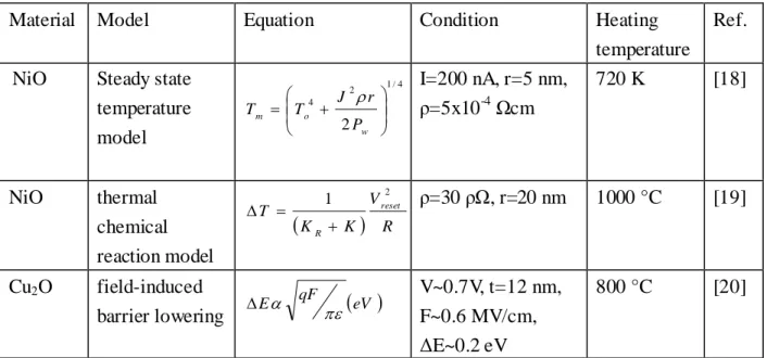
Table. 1-1 Comparison on the estimated heating temperature of different 71 material.
Figure Caption
Chapter 1
Fig. 1-1 DRAM cell with 1T1C structure. 62
Fig. 1-2 SRAM CMOS cell with six-transistor (6T) configuration example 62 Fig. 1-3 Schematic cross section of a floating-gate Flash memory 6 3 Fig. 1-4 (a) The ferroelectric compositional structure of a perovskite crystal 63
unit cell. (b) The schematic diagram of the typical hysteresis curve related to the moving atoms under the applied bias. (c) Polarization versus temperature curve.
Fig. 1-5 Illustration of the low resistance state (parallel direction) and high 65 resistance state (antiparallel direction) of the MRAM device.
Fig. 1-6 (a) Schematic diagram for the phase change memory cell consisting 65 of Ge2Sb2Te5 material [13]. (b) According to the Monte Carlo
model simulation for crystallization, the phase change in resistance values as a function of time can be shown. Crystal grains are in blue, amorphous phase in red [14]. (c) Temperature-time relationship in SET and RESET pulse operation. [13]
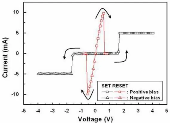
Fig. 1-7 Two types of differential negative resistance for (a) voltage 66 controlled mode (N shape) and (b) current controlled mode (S shpae). Fig. 1-8 The typical Unipolar I-V curves. The arrows indicate the sweep 67
current loop.
Fig. 1-9 The typical bipolar I-V curves at (a) clockwise current loop and 68 (b) counterclockwise current loop.
Fig. 1-10 Schematic illustration of conduction processes in the high-field 69 region of a metal-oxide-metal structure.
Fig. 1-11 Energy diagram showing the position of the stored charge relative to 70 the Fermi level: (a) at a voltage bias of V volts, (b) immediately
after voltage has been rapidly reduced to zero, (c) after a longer time interval. [16]
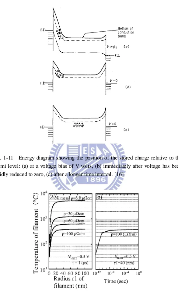
Fig. 1-12 (a) Temperature of filament as a function of filament radius with 70 different resistivity values. (b) The relation between temperature
of filament and measured time for 40 nm radius and resistivity = 100 μΩ.
Fig. 1-13 Simulation test on two reset/set cycles of C-RRAM. (a) the applied 71 voltage as a function of temperature, (b) distribution of the a
tomic structure in the simulated filaments, and (c) temperature distribution among the entire TMO film. [21]
Fig. 1-14 Surface morphology (a),(c),(e) and its corresponding current images 72 (b),(d),(f) are shown by AFM and C-AFM measurement,
respectively. Operation condition of the (a)(b) SET scan under 2.3 V bias, (c)(d) RESET scan under 1.5 V bias, and (e)(f) SET scan under 2.3 V bias. [32]
Fig. 1-15 (a) A schematic diagram showing the sample geometry. (b) 72 Simulation on temperature as a function of measured time at the
filament center under applied bias. Temperature distribution for the case with (c) 200 nm and (d) 10 nm bottom Pt electrode. [33]
Fig. 1-16 (a) Typical I-V curve of NiO film. Cross-sectional TEM images 73 of the Pt/NiO/Pt structure of (b) pristine, (c) LRS, and (d) HRS. [18] Fig. 1-17 Schematic diagram of the MIM stacked structure. 73 Fig. 1-18 (a) Resistive switching test of NiO films with Au, Pt, or Al as 73
top electrode. (b) Al/NiO/Pt and (c) Al/NiO/Pt structures. The arrows indicates the sweeping directions of applied bias. [35]
Fig. 1-19 Ellingham diagram reveals the free energies for oxidation of the 74 various metals. [37]
Fig. 1-20 Cross-sectional TEM image and corresponding EDX analysis of 74 NiPt/NiO/NiPt thin film (a) beform forming and (b) after forming. Ni penetration into the NiO film after forming process was
clearly observed. [57]
Fig. 1-21 The EDX analysis in STEM mode for detection on the atomic 75 materials. Four places were detected for investigation the Ag
bridge involving inside the TMO films. (a) out side the Ag bridge, (b) in the middle of the Ag bridge, (c) near the Pt electrode, and (d) a line profile for showing the intensity of Ag atoms along the bridge. [94]
Fig. 1-22 A schematic diagram for the resistive switching mechanism of the 75 electrometallization memory. (a) Oxidation of Ag atoms at anode, (b) migration of Ag cations toward the cathode and their reduction process, (c) The precipitations of Ag atoms connect the anode and cathode and form a metallic Ag conducting bridge. And (d) the electrochemical dissolution of Ag bridge takes place. [94]
Fig. 1-23 SEM images showing the Ag dendrite growth under the applied bias 76 of -1 V for about (a) 0 s, (b) 1 s, (c) 2 s, and (d) 4 s, respectively. [98] Fig. 1-24 Schematic diagram of Pt/Nb:STO Schottky junction for indicating 76
the Schottky barrier height modulated by the trapped electrons. [105] Fig. 1-25 Schematic diagram of the three domains model. The insulator film 77
can be regarded as top, middle, and bottom domains, respectively. The tunneling amplitudes between two domains regulate the injected carriers. [119]
Fig. 1-26 (a) virgin resistance vs. WF, and (b) virgin resistance vs. free 77 energy. [142]
Fig. 1-27 I-V characteristics for (a) Ag, Cu, Au, Pt/PCMO/Pt, 77 (b) Al/PCMO/Pt, (c) Ti/PCMO/Pt, and (d) Ta/PCMO/Pt. The
switching loop is followed by 0 V → 3 V → -3 V → 0 V. The cross-sectional HRTEM images at right side are the corresponding microstructure. [142]
Fig. 1-28 Bubble gas observation at (b),(c) negative bias, then at (d)-(h) 78 positive bias. (g) The eruption features observed by atomic force
micrograph after bias voltage was removed. [191]
Fig. 1-29 The schematic diagram is shown for (a) ohmic conduction, (b) 78 Schottky emission, (c) Frenkel emission, and (d) Fowler-Nordheim Tunneling.
Chapter 3
Fig. 3-1 The forming characteristics of the HfOx samples fabricated with 141
different composition reactants ratio of HfCl4 : H2O = 5 : 2 or 5 : 3
during ALD process.
Fig. 3-2 The high and low resistance values of HfOx/TiN device with 141
different composition reactants ratio of HfCl4 : H2O = 5 : 2 or
5 : 3 during ALD process
Fig. 3-3 The operation voltage percentage distribution of the HfOx 142
samples fabricated with composition reactants ratio of HfCl4 : H2O = 5 : 2 during ALD process.
Fig. 3-4 The operation voltage percentage distribution of the HfOx 142
samples fabricated with composition reactants ratio of HfCl4 : H2O = 5 : 3 during ALD process.
Fig. 3-5 The resistive switching behaviors of HfOx/TiN device using Pt, 143
Ni, and Ti top metal electrode.
Fig. 3-6 The resistance values of high and low resistance state at 0.1 V 143 of HfOx/TiN device using Pt, Ni, and Ti top metal electrode.
electrode TE=Pt, Ni, Ti and Al.
Fig. 3-8 XPS core level spectra of (a) Pt 4f and (b) Ti 2p at the interface 145 region. AES depth profile of (c) Pt/HfOx/TiN and (d) Ti/HfOx/TiN
structure.
Fig. 3-9 Accumulative percentage of the operation voltage of Ni/HfOx/TiN 147
and Ti/HfOx/TiN capacitor device.
Fig. 3-10 Data retention test result of both high and low resistance values at 147 0.1 V of Ni/HfOx/TiN and Ti/HfOx/TiN capacitor device.
Fig. 3-11 The continuous unipolar resistive switching I-V curves in 148 (a) Pd/HfOx/TiN and (b) Pd/Al(50Å)/HfOx/TiN capacitor device.
Fig. 3-12 (a) Accumulative percentage of the operation voltage of 149 Pd/HfOx/TiN and Pd/Al(50Å)/HfOx/TiN capacitor device.
(b) Endurance test of Pd/HfOx/TiN (left) and
Pd/Al(50Å)/HfOx/TiN (right) capacitor device at 0.4V.
Fig. 3-13 The cross-sectional TEM iamge of the Pd/Al(35Å)/HfOx/TiN 150
structure.
Fig. 3-14 (a) The resistive switching behaviors of the Pd/HfOx/TiN device 151
with Al layer inserted of 35Å, 70Å, and 100Å. (b) Comparison of the endurance test of Pd/HfOx/TiN device with Al layer inserted
of 35Å, 70Å, and 100Å.
Fig. 3-15 Depth profiling of Al 2p core level spectra of Pd/HfOx/TiN 152
structures with thickness of (a) 35Å Al layer inserted after every 2 min Ar+ ion sputtering. As going from the bottom to the top, the spectra describe spectral changes from the top to the bottom electrode. The O 1s spectra of (b) Step B was also analyzed, and deconvoluted to fit the spectra into the two peak (530.7 and
531.7 eV), which correspond to HfO2 and Al2O3 states, respectively.
Depth profiling of Al 2p core level spectra of Pd/HfOx/TiN
structures with thickness of (c) 150Å Al layer inserted after every 2 min Ar+ ion sputtering. As going from the bottom to the top, the spectra describe spectral changes from the top to the bottom electrode. The O 1s spectra of (d) Step H was also analyzed, and deconvoluted to fit the spectra into the two peak (530.7 and 531.7 eV), which correspond to HfO2 and Al2O3 states, respectively.
Fig. 3-16 (a) AFM image of the as-grown HfOx films. (b) AFM image of 154
the as-grown HfOx films under Ar RTA 400 °C for 90 seconds.
(c) AFM image of the as-grown HfOx films under Ar RTA 500 °C
Fig. 3-17 Comparison on the forming process of Ni/HfOx/TiN samples 155
under different Ar RTA treatment conditions.
Fig. 3-18 (a) XRD patterns of the HfOx-based memory devices at various Ar 156
RTA temperatures and treatment time. (b) XRD patterns of the HfOx-based memory devices changes to strong (023) orientation
when treated under longer treatment time.
Fig. 3-19 The resistive switching behaviors of the Ni/HfOx/TiN structures at 157
different Ar RTA temperature for 90 seconds.
Fig. 3-20 The high and low resistive values at 0.1 V of the Ni/HfOx/TiN 157
structures at different Ar RTA temperature for 90 seconds.
Fig. 3-21 The SET and RESET voltage distribution of the Ni/HfOx/TiN 158
structures at different Ar RTA temperature for 90 seconds.
Fig. 3-22 The distribution of the maximum reset current of the Ni/HfOx/TiN 158
structures at different Ar RTA temperature for 90 seconds.
Fig. 3-23 Relative unipolar resistive switching curves of the Ni/HfOx/TiN 159
devices at various RTA treatment conditions in O2 ambient for
400 °C.
Fig. 3-24 Endurance characteristics of the Ni/HfOx/TiN devices at various 159
RTA treatment conditions in O2 ambient for 400 °C.
Fig. 3-25 Operation voltage values distribution of the Ni/HfOx/TiN devices 160
at various RTA treatment conditions in O2 ambient for 400 °C.
Fig. 3-26 AES depth profile of the Ti/HfOx/TiN structure. 160
Fig. 3-27 Comparison on the Ireset(max) of the Ni/HfOx/TiN devices at 161
various RTA treatment conditions in O2 ambient for 400 °C.
Fig. 3-28 Comparison on the RESET switching power of the Ni/HfOx/TiN 161
devices at various RTA treatment conditions in O2 ambient for
400 °C.
Fig. 3-29 (a) XPS spectra of Hf 4f5/2, 4f7/2 and Hf4+ 4f5/2, 4f7/2. (b) XRD 162
patterns of HfOx thin films deposited on the TiN/SiO2/Si substrate.
Multiple red lines represent the intensity of various orientation peaks of the HfO2 film.
Fig.3-30 I-V characteristics of the Pt(E)/HfOx/TiN sample using the (a) 163
voltage mode operation for SET and RESET process, (b) current mode operation for SET and voltage mode for RESET processes under current compliance of 0.5 mA, and (c) current mode operation for SET under current compliance of 50 μA.
Fig. 3-31 Typical I-V curves of 4 consecutive sweeping cycles under 164 voltage-mode operation of (a) Pt(S)/HfOx/TiN,
(b) Pt(E50+S)/HfOx/TiN, and (c) Pt(E150+S)/HfOx/TiN devices.
Fig. 3-32 High (empty) and low (solid) resistance value distribution of 165 Pt(S)/HfOx/TiN (upward-triangle, black), Pt(E50+S)/HfOx/TiN
(downward-triangle, red), and Pt(E150+S)/HfOx/TiN device
(circle, blue).
Fig. 3-33 Schematic illustration of the generation and primary collision 166 process of the sputtered particles (Ar+, Aro, O-) in the sputtered-
deposited films. After, energetic incident Ar ions are neutralized and reflected at the cathode (target) surface where they collide with the film surface to induce film damage.
Fig. 3-34 Typical I-V curves of several consecutive sweeping cycles under 167 current-mode operation of (a) Pt(S)/HfOx/TiN, (b)
Pt(E50+S)/HfOx/TiN, and (c) Pt(E150+S)/HfOx/TiN device.
Fig. 3-35 (a) The transmittance of ITO/glass structure. (b) The I-V curves 168 of forming process with UV light exposure, and each symbol
represents different exposure condition: Untreated (square), #1-30s (up-triangle), #1-120s (down-triangle), and #2-120s (circle), respectively.
Fig. 3-36 The typical I-V characteristics of ITO/HfOx/TiN device after 169
applying 1st, 50th, and 100th voltage sweeping cycles of (a) untreated sample and (b) under of UV light exposure of 120s, respectively.
Fig. 3-37 Reset/set cycling endurance of ITO/HfOx/TiN device of (a) 170
untreated, and (b) under UV light exposure of 120 seconds (#2-120s), respectively.
Fig. 3-38 Resistance distribution of HRS (solid) and LRS (empty) for 171 ITO/HfOx/TiN device of untreated (square), under UV light
exposure for 120 (circle), and 300 seconds (down triangle).
Fig. 3-39 (a) The I-V curves of Shielded UV-120 s device. (b) The I-V 172 curves of Unshielded UV-120 s device.
Fig. 3-40 Evolution of high and low resistance state during sequent 173 voltage sweeping of Shielded UV-120 s and Unshielded
UV-120 s samples.
Fig. 3-41 Distribution of SET and RESET voltages versus switching cycles 174 of (a) the Shielded UV-120 s devices, and (b) the Unshielded
UV-120 s devices.
Fig. 3-42 Schematic diagrams show Shielded UV-120 s samples (a) after 175 UV light exposure and (b) filament formation, and Unshielded
UV-120 s samples (c) after UV light exposure and (d) filament formation.
Fig. 3-43 The switching behaviors of the Pd/HfOx/TiN and 176
Pd/Al/HfOx/TiN structure operated by negative bias for SET
and positive one for RESET.
Fig. 3-44 The switching behaviors of the Pd/HfOx/TiN structure operated 176
by negative bias for SET and positive one for RESET (up-triangle) and positive for SET and negative for RESET (down-triangle).
Fig. 3-45 XPS core level spectra of (a) Pt 4f and (c) Al 2p at the interface 177 region. AES depth profile of (b) Pt/HfOx/TiN and (d) Ti/HfOx/TiN
structure.
Fig. 3-46 Evolution of ON-state and OFF-state during sequent voltage 179 sweeping.
Fig. 3-47 Distribution of the SET and RESET voltage in Pd/Al/HfOx/TiN 179
devices under the two polarity of resistive switching operation.
Chapter 4
Fig. 4-1 The XPS spectra of the Gd 4p peaks at the initial resistance state. 201 Fig. 4-2 The XPS spectra of the Gd 4p peaks at the low resistance state. 201 Fig. 4-3 Typical unipolar I-V characteristics of RRAM device based on 202
Ti/Gd2O3/Pt capacitor structures. Blue line represents the forming
process. Red and black lines represent I-V characteristics under the positive and negative bias operation, respectively.
Fig. 4-4 I-V curves of continuous three switching cycles of the Ti/Gd2O3/Pt 203
capacitor structures under positive bias operation.
Fig. 4-5 I-V curves of continuous three switching cycles of the Ti/Gd2O3/Pt 203
capacitor structures under negative bias operation.
Fig. 4-6 Endurance test of the Ti/Gd2O3/Pt capacitor structures under a 204
positive bias operation.
Fig. 4-7 Distribution of the Vset and Vreset of the Ti/Gd2O3/Pt capacitor 204
structures under positive bias operation (up-triangle) and negative bias operation (square).
Fig. 4-8 XPS Ti 2p 3/2 level spectra fitted with Gaussian function of Ti0+, 205
Ti0.5+, and Ti+ peak.
Fig. 4-9 Schematic pictures of the Pt/Ti/Gd2O3/Pt structure operated under 206
(a) SET, and (b) RESET process under positive bias, and (c) SET, and (d) RESET process under negative bias operation. Solid and
empty circle symbols represent the oxygen ions and oxygen vacancies, respectively.
Fig. 4-10 I-V characteristics of the Ti/Gd2O3/Pt device plotted in 207
ln (I) – ln (V) scale. Both HRS and LRS are included on the plot.
Fig. 4-11 The XRD patterns of the ITO/Gd2O3/ITO devices. 208
Fig. 4-12 Enlarge image of the XRD patterns of the ITO/Gd2O3/ITO devices. 208
Fig. 4-13 Surface morphology image of the Gd2O3 films grown at 25 °C. 209
Fig. 4-14 Surface morphology image of the Gd2O3 films grown at 200 °C. 209
Fig. 4-15 Surface morphology image of the Gd2O3 films grown at 300 °C. 209
Fig. 4-16 Cross-sectional TEM image of the ITO/Gd2O3/ITO films grown 210
at 25 °C.
Fig. 4-17 Cross-sectional TEM image of the ITO/Gd2O3/ITO films grown 210
at 300 °C.
Fig. 4-18 Transmittance of the ITO/Gd2O3/ITO structure grown at various 211
growth temperature of 25, 200, and 300 °C under wavelength of visible light in the range of 400-800 nm.
Fig. 4-19 The logo under this transparent ITO/Gd2O3/ITO structure is 211
clearly been seen.
Fig. 4-20 I-V curves of the Gd2O3 films grown at various growth 212
temperature of 25, 200, and 300 °C.
Fig. 4-21 Endurance test of the Gd2O3 films grown at various growth 212
temperature of 25, 200, and 300 °C.
Fig. 4-22 XPS spectra of Gd 4d3/2, 4d5/2 and Gd3+ 4d3/2, 4d5/2 of the 213
Gd2O3 films grown at 25 °C.
Fig. 4-23 XPS spectra of Gd 4d3/2, 4d5/2 and Gd3+ 4d3/2, 4d5/2 of the 213
Gd2O3 films grown at 300 °C.
Fig. 4-24 Resistance values of IRS, HRS, and LRS according to 214 temperature of the Gd2O3 films grown at 300 °C.
Fig. 4-25 Cell size versus respective IRS and LRS resistance values 214 measured at 0.4 V of the Gd2O3 films grown at 300 °C.
Fig. 4-26 Surface morphology image of the Gd2O3 films grown at 300 °C. 215
Fig. 4-27 Resistive switching test by applying fixed -2 V for SET but 216 varying the RESET voltage bias from +0.8 to +2.4 V.
Fig. 4-28 LRS to HRS current ratio at 0.1 V as a function of SET voltage. 216 Fig. 4-29 Resistive switching test by applying fixed 2 V for RESET but 217
varying the SET voltage bias from -0.6 to -2.6 V.
Fig. 4-30 LRS to HRS current ratio at 0.1 V as a function of RESET voltage. 217 Fig. 4-31 I-V characteristics of both positive and negative bias regions 218
of the ITO/Gd2O3/ITO device plotted in a ln (|J|) - ln (|V|) curve.
Both ON-state and OFF-state are included on this plot.
Chapter 5
Fig. 5-1 AFM image of the LaAlO films grown at oxygen partial pressure 254 of 7×10⁻³ torr.
Fig. 5-2 AFM image of the LaAlO films grown at oxygen partial pressure 254 of 1.4×10⁻² torr.
Fig. 5-3 AFM image of the LaAlO films grown at oxygen partial pressure 254 of 2.8×10⁻² torr.
Fig. 5-4 Schematic diagram depicts the pulsed laser deposition fabrication 255 process in low oxygen partial pressure.
Fig. 5-5 Schematic diagram depicts the pulsed laser deposition fabrication 255 process in high oxygen partial pressure.
Fig. 5-6 Surface morphology image of the LaAlO films grown at oxygen 256 partial pressure of 7×10⁻³ torr.
Fig. 5-7 Surface morphology image of the LaAlO films grown at oxygen 256 partial pressure of 1.4×10⁻² torr.
Fig. 5-8 Surface morphology image of the LaAlO films grown at oxygen 256 partial pressure of 2.8×10⁻² torr.
Fig. 5-9 (a) The La 4d spectrum of LAO deposited at various oxygen 257 pressure. (b) The Al 2p spectrum of LAO deposited at various
oxygen pressure.
Fig. 5-10 High resolution cross-sectional TEM image of the LaAlO films 258 grown at oxygen partial pressure of 7×10⁻³ torr.
Fig. 5-11 High resolution cross-sectional TEM image of the LaAlO films 258 grown at oxygen partial pressure of 1.4×10⁻² torr.
Fig. 5-12 High resolution cross-sectional TEM image of the LaAlO films 258 grown at oxygen partial pressure of 2.8×10⁻² torr.
Fig. 5-13 Transmittance of the ITO/LAO/ITO structure grown at various 259 oxygen pressure of 7×10⁻³ (L-7), 1.4×10⁻² (L-14), and 2.8×10⁻²
(L-28) torr under wavelength of visible light in the range of 400-800 nm.
Fig. 5-14 (a) Leakage current I versus electric field of LAO films deposited 260 at various oxygen pressures. (b) Comparison on the breakdown
(BD) voltages of LAO films deposited at various oxygen pressures. Fig. 5-15 (a) Leakage current I versus electric field of LAO films 261
deposited at various oxygen pressures. (b) Comparison on the breakdown (BD) voltages of LAO films deposited at various oxygen pressures.
Fig. 5-16 Forming voltages for the LAO films grown at oxygen pressure 262 of (a) 7×10⁻³ torr, (b) 1.4×10⁻² torr, and (c) 2.8×10⁻² torr at various measured temperature.
Fig. 5-17 Plots of ln J vs ln V curve for the LAO films grown at oxygen 263 pressure of (a) 7×10⁻³ torr, (b) 1.4×10⁻² torr, and (c) 2.8×10⁻² torr
Fig. 5-18 The ln (|I|) values versus T-1/4 for the LAO films grown 264 at different oxygen pressure.
Fig. 5-19 Plots of ln (J/T2) vs E1/2 curve for the LAO films grown at 265 oxygen pressure of (a) 7×10⁻³ torr, (b) 1.4×10⁻² torr, and (c)
2.8×10⁻² torr
Fig. 5-20 (a) Variations of ln (J/T2) with 1/T of the ITO/LAO(L-7)/ITO 266 capacitor, where the J represents the measured value at voltages
over the range of 1 to 5 V. (b) Variation in activation energies of the ITO/LAO(L-7)/ITO capacitor as a function of V1/2.
Fig. 5-21 (a) Variations of ln (J/T2) with 1/T of the ITO/LAO(L-28)/ITO 267 capacitor, where the J represents the measured value at voltages
over the range of 1 to 5 V. (b) Variation in activation energies of the ITO/LAO(L-28)/ITO capacitor as a function of V1/2.
Fig. 5-22 (a) Plots of ln (J/V) vs V1/2 curve for the LAO films grown 268 at oxygen pressure of 7×10⁻³ torr. (b) Variations of ln (J/V) with
1/T of the ITO/LAO/ITO capacitor, where the J represents the measured value at voltages over the range of 6 to 9 V. (c) Variation in activation energies of the ITO/LAO/ITO capacitor as a function of V1/2.
Fig. 5-23 (a) Plots of ln (J/V) vs V1/2 curve for the LAO films grown 269 at oxygen pressure of 2.8×10⁻² torr. (b) Variations of ln (J/V)
with 1/T of the ITO/LAO/ITO capacitor, where the J represents the measured value at voltages over the range of 6 to 9 V. (c) Variation in activation energies of the ITO/LAO/ITO capacitor as a function of V1/2.
Fig. 5-24 I-V curves of LAO-based memory device grown at various 271 oxygen pressures.
Fig. 5-25 The resistance values of both ON-state and OFF-state at 271 0.1 V of LAO-based memory device grown at (a) 7×10⁻³ torr,
Fig. 5-26 Vset and Vreset distribution among 500 switching cycles 273
of LAO-based memory device grown at (a) 7×10⁻³ torr, (b) 1.4×10⁻² torr, and (c) 2.8×10⁻² torr.
Fig. 5-27 Schematic diagrams for resistive switching mechanism in 274 ITO/LAO/ITO structure on forming process (a) at low voltage
bias (initial), (b) at middle voltage bias (|-0.7| V < V < |-8| V), (c) at large voltage bias (V > |-8 V|) to LRS. Under the positive bias, the oxygen ions can migrate back to reoxidize in the insulator film. (d) and (e) represent different HRS picture of the insulative matrix.
Fig. 5-28 Schematic diagrams for resistive switching mechanism in 275 ITO/LAO/ITO structure on forming process (a) at low voltage
bias (initial), (b) at middle voltage bias (|-0.7| V < V < |-8| V), (c) at large voltage bias (V > |-8 V|). Under the positive bias, the oxygen ions can migrate back to reoxidize in the insulator film. (d) and (e) represent different HRS picture of the insulative matrix.
Fig. 5-29 (a) The I-V curves operate at fixed Vreset = 2 V and varying 276
Vset from -0.5 to -10 V of LAO-based memory grown at
oxygen pressure of 7×10⁻³ torr. (b) Resistance values of HRS and LRS as a function of Vset of LAO-based memory grown
at oxygen pressure of 7×10⁻³ torr.
Fig. 5-30 (a) The I-V curves operate at fixed Vreset = 2 V and varying 277
Vset from -0.5 to -10 V of LAO-based memory grown at
oxygen pressure of 1.4×10⁻² torr. (b) Resistance values of HRS and LRS as a function of Vset of LAO-based memory grown
at oxygen pressure of 1.4×10⁻² torr.
Fig. 5-31 (a) The I-V curves operate at fixed Vreset = 2 V and varying 278
Vset from -0.5 to -10 V of LAO-based memory grown at
oxygen pressure of 2.8×10⁻² torr. (b) Resistance values of HRS and LRS as a function of Vset of LAO-based memory grown
at oxygen pressure of 2.8×10⁻² torr.
Fig. 5-32 (a) The I-V curves operate at fixed Vset = -3 V and varying 279
Vreset from 1 to 4 V of LAO-based memory grown at oxygen
pressure of 7×10⁻³ torr. (b) Resistance values of HRS and LRS as a function of Vreset of LAO-based memory grown at oxygen
pressure of 7×10⁻³ torr.
Vreset from 0.6 to 3 V of LAO-based memory grown at oxygen
pressure of 1.4×10⁻² torr. (b) Resistance values of HRS and LRS as a function of Vreset of LAO-based memory grown at oxygen pressure of 1.4×10⁻² torr.
Fig. 5-34 (a) The I-V curves operate at fixed Vset = -3 V and varying 281
Vreset from 0.2 to 3 V of LAO-based memory grown at oxygen
pressure of 2.8×10⁻² torr. (b) Resistance values of HRS and LRS as a function of Vreset of LAO-based memory grown at oxygen pressure of 2.8×10⁻² torr.
Fig. 5-35 (a) Schematic diagrams for the measurement test. (b) 282 Effective schematic diagrams for illustrating the measurement
test.
Fig. 5-36 Evolution on the resistance values of A-B, A-G, and B-G 282 measuring test.
Fig. 5-37 The I-V curves of (a) L-7 sample, (b) L-14 sample, and (c) 283 L-28 sample.
Fig. 5-38 Schematic diagram for the configuration of random 284 resistor network model for (a) IRS, (b) LRS, and (c) HRS.
Fig. 5-39 The ON and OFF resistance values (left y-axis) and the 284 ON/OFF ratios (right y-axis) as a function of compliance
current.
Fig. 5-40 Electrical curves fitting on the (a) negative and (b) positive 285 side of the I-V switching curves on L-7 samples.
Fig. 5-41 Electrical curves fitting on the (a) negative and (b) positive 286 side of the I-V switching curves on L-28 samples.
Fig. 5-42 (a) Data retention test of both HRS and LRS of (a) L-7, (b) 287 L-14, and (c) L-28 sample. All the samples can maintain its
data over 10000 s at 0.1 V.
Chapter 1 Introduction
1.1 Introduction of Memory
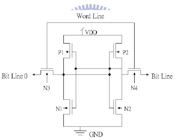
Memory can be easily divided into two main categories: volatile and nonvolatile. Volatile memory loses data when the applied bias is turned off. A constant power is required to maintain the stored data. There are two main types of random access memory (RAM), namely, dynamic random access memory (Dynamic Random Access Memory, DRAM) and static random access memory (Static Random Access Memory, SRAM), that belong to this category (Figs. 1.1 and 1.2, respectively). The unit size of a DRAM cell is composed of a transistor and a capacitor (1T1C). It has only a small device size (6-12F2) [1] in which high device density and high capacity can be achieved on a DRAM array cell. Therefore, DRAM has a lower cost per bit than memories with less compact array, in addition to faster access speed, giving it a high performance rating. However, the charge decays away in a finite length of time (milliseconds); a periodic refresh is needed to restore the charge for a DRAM to retain its memory. As for a conventional SRAM cell (50-80F2) [2], it consists of a basic flip-flop circuit that needs only a DC current applied to retain its memory. It contains four transistors plus either two transistors or two polysilicon-load resistors as pull-up devices (Fig. 1-2). No periodic refresh is required, thereby eliminating the need for external address counters and refreshing circuitry used in DRAM. Nevertheless, SRAM is larger than a basic cell, which makes it more expensive to build, has higher power consumption because DC power should be applied continuously, and, historically, has a slower speed.
1.1.1 Nonvolatile memory
programmable read only memory (EPROM), and electrically erasable programmable ROM (EEPROM). NVM does not lose stored data when the power is turned off. ROM is preprogrammed in a silicon by the semiconductor manufacturer using a program pattern supplied by an ROM user. ROMs have the advantages of being manufactured using a relatively low technology and inexpensive process. Conversely, aside from the fact that their contents cannot be altered, ROMs require a high initial, one-time cost to produce a custom product. On the other hand, EPROM has provided a solution to address the erasable requirement. EPROM has a cell containing a select and a storage transistor that holds excess charge when programmed, which can be erased and reprogrammed by the user. EPROMs are more expensive than ROMs in per-unit cost for volume quantities, but are a solution to the need for a reprogrammable nonvolatile memory. However, there are several disadvantages to EPROMs. They are not as fast in performance as RAMs or ROMs, and they cannot be reprogrammed in the system. Normally, they must be removed from the system manually and reprogrammed using special ultraviolet (UV) light equipment to erase the old programming followed by another piece of equipment to program the new. EPROMs are in ceramic packages with quartz windows that can be damaged by automated insertion equipment and thus must be hand inserted in the sockets.
The shortcomings of EPROM have been overcome by a relative newcomer to the memory arena, EEPROM. EEPROM can be electrically erased in the system; thus, the need to buy expensive ultraviolet erase equipment is eliminated. EEPROMs are available in standard plastic packages without the quartz window, which eliminates light-sensitivity problems and enables the EEPROMs to be inserted in high-volume applications using an automated insertion equipment. It also erases considerably faster than EPROM, that is, a few milliseconds is needed for EEPROM, whereas half hour is required for EPROM. However, the memory density of EEPROM is lower than that
of EPROM. This shortcoming limits the application of EEPROM to lower storage capacity equipments only. Several variations of this technology include metal nitride oxide semiconductor (MNOS), silicon oxide nitride oxide semiconductor (SONOS), floating gate tunneling oxide (FLOTOX), and textured polysilicon.
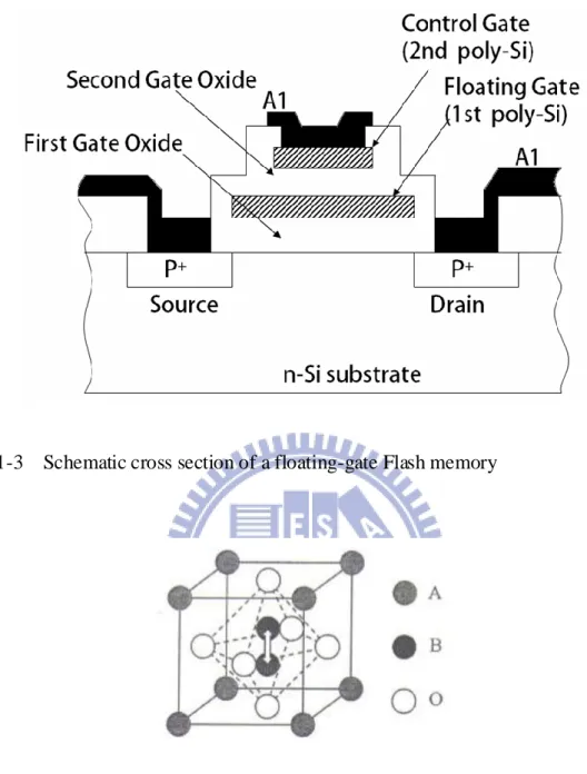
Flash memories based on EPROM or EEPROM technologies are devices for which contents of all memory array cells can be erased simultaneously, unlike the EEPROMs that have select transistors incorporated in each cell to allow for the individual byte erasure. The mainstream NVM today in the market is flash memory, which provides wide application and a technology driver for the global semiconductor. Flash memories include NOR flash and NAND flash, and provides the functionality of different products requirements. NOR flash is more suitable for code storage applications, such as mobile phones and DVD players. NAND flash has higher density and is used for data storage market for emerging applications, such as PDA, memory cards, MP3 audio players, digital cameras, and USB flash personal discs. An additional gate called floating gate was embedded between the poly gate and the gate oxide in the traditional metal-oxide-semiconductor field effective transistor (MOSFET) invented by S. M. Sze and D. Kahng in 1967 [3]. The structure of the conventional floating-gate device is shown in Fig. 1-3. The floating gate can store electrons and is electrically governed by a capacitively coupled control gate. By controlling the numbers of injected electrons inside the floating gate, different threshold voltage of the flash memory can be obtained. This method is used to determine different states, which is based on whether charges are stored in the floating gate or not.
Recently, however, some bottlenecks of flash memory have been identified, such as high operation voltage, low operation speed, and poor retention time. To improve the switch speed of a flash memory, the thickness of tunnel oxide must be reduced.
The tunnel oxide of the conventional flash memory must maintain an appropriate thickness to provide superior isolation under retention, endurance, and disturbed conditions to keep the data storage invariable for 10 years. Hence, there is a tradeoff between switch speed and reliability for the optimum thickness of tunnel oxide. Some advanced flash memories, such as charge-trapping flash and band-engineered SONOS flash, have been proposed to satisfy the continuous shrinking demand [4,5]. Currently, several groups are eagerly finding the emerging next-generation NVMs that have high density, high speed, and nonvolatility. There are four possible candidates for the next-generation NVMs: ferroelectric random access memory (FRAM) [6-8], magnetroresistive random access memory (MRAM) [9-11], phase change random access memory (PCRAM) [12-14], and resistive random access memory (RRAM).
1.1.2 Next-generation NVM (a) FRAM
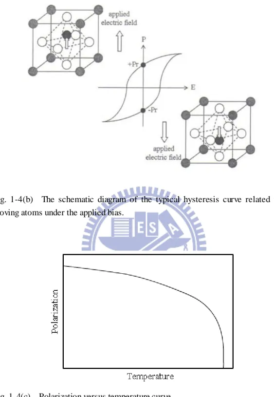
FRAM is a NVM based on the ferroelectric effect of the charge storage mechanism, and is quite different from the floating-gate-based NVM. Typical perovskite ferroelectric materials are BaTiO3, PbTiO3, PZT (PbZr1-xTixO3), PLZT
(Pb1-xLxZrO3), PMN (PbMg1-xNbxO3), SBT (SrBi2Ta2O9), SBN (SrBi2Nb2O9), and
among others. The ferroelectric effect is the ability of a material to store an electric polarization in the absence of an applied electric field. A FRAM device cell is fabricated by depositing a ferroelectric film in crystal form between two electrode plates to form a capacitor. The perovskite crystals of a ferroelectric material maintain two stable polarization states resulting from the alignment of internal dipoles, corresponding to states of logical ―1‖ and ―0,‖ which in turn reverses the alignment of these internal dipoles. A simplified model of a ferroelectric crystal is shown in Fig. 1-4(a) [6]. A mobile atom is in the center of the crystal, and application of an electric
field across the face of the crystal causes this atom to move in the direction of the field. A reversal of the field causes the atom to move in the opposite direction, resulting in a typical hysteresis curve, as shown in Fig. 1-4(b). The positions of the atom at top and bottom of the crystal are stable, and the atom remains in these states when the external field is removed. No external electric field or current is required for the ferroelectric material to remain polarized in either state; hence, a memory device can be built for storing digital (binary) data that will not require power to retain information stored within it. The critical temperature for ferroelectric materials is known as the Curie temperature; the perovskite structure assumes a cubic symmetry and is paraelectric when the Curie temperature is exceeded, that is, the films will lose the ferroelectric behavior. Therefore, the Curie temperature for a ferroelectric material must be high enough to maintain a wide margin of the application in semiconductor technology. The polarization versus temperature curve is shown in Fig. 1-4(c) [7,8]. To read a FRAM, detecting the position of the atoms within the petrovskite crystals is necessary. However, it cannot be directly sensed. The read operation involves applying an electric field across the capacitor, causing the mobile atoms to move across the crystals in the direction of the field if they are not already in the appropriated positions. The circuit dumps charge resulting from the applied field from the capacitor and compares it to the charge from a reference. A capacitor with atoms that switch states will emit a larger charge than a capacitor with atoms that do not switch. The memory sensing circuitry must determine which capacitors switched. The ―switched charge‖ allows the circuit to determine the state of the memory cell. Given that a memory read operation involves a change of state, the FRAM circuitry must restore the original memory state. Therefore, each read access is accompanied by a pre-charge operation that restores the memory states. To write a FRAM, no system overhead is required, and the operation is very similar to a read operation. The circuit
applies write data to the ferroelectric capacitors, and the new data switches (if necessary) the state of the ferroelectric crystals.
(b) MRAM
MRAM is solid state, nonvolatile magnetic storage device in which the stored data are represented by the magnetization direction and the readout is done by resistance measurements. According to the proponents of MRAM, this technology scales better to low voltages than DRAM, SRAM, and flash memories, and it requires fewer mask steps than the DRAM process. Early MRAMs were based on the anisotropic magnetoresistance (AMR) effect. Only less than 5% of the amplitude of the AMR effect in thin films limits the application only to military and space application. In 1988, the discovery of the giant magnetoresistive (GMR) effect [9] changed this situation. This GMR technology (5-15%) has been applied in commercial products like hard disk drive (HDD) read heads and magnetic sensors. A breakthrough in the field of magnetic tunnel junctions was achieved sometime in 1995, when the large tunnel magnetoresistive (TMR) effect [10] was demonstrated at room temperature, further contributing to the development of MRAM. The TMR has the potential of reaching MR ratios of 30-40%. However, a tougher challenge lies in finding the right process recipe that would enable the production of reliable MRAMs.
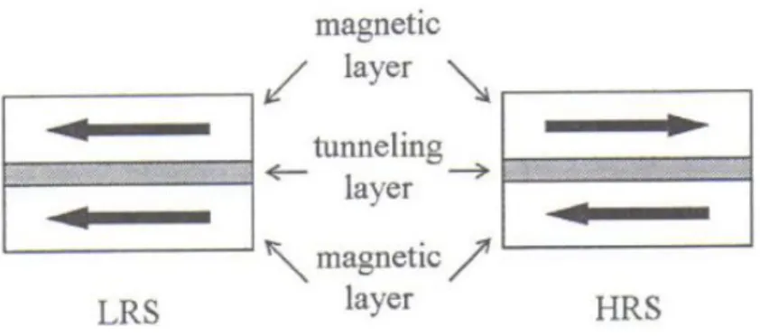
In general, both GMR and TMR result in low resistance if the magnetization directions in the multilayer are parallel, and in high resistance when the magnetizations are anti-parallel. For the representation of storage bits, different possibilities exist. The pseudo-spin valves use two ferromagnetic layers that switch their magnetization direction at different magnetic fields, which can be accomplished by utilizing layers of different magnetic materials, or layers of the same material but of different thicknesses. A typical structure of MRAM cell is shown in Fig. 1-5.
The resistance of two thin ferromagnetic layers separated by a thin nonmagnetic conducting layer can be altered based on whether the moments of ferromagnetic layers are parallel or anti-arallel. The layers with parallel magnetic moments will have less scattering at the interface, longer mean free paths, and lower resistance. On the other hand, the layers with antiparallel magnetic moments will have more scattering at the interfaces, shorter mean free paths, and higher resistance. In order for the spin-dependent scattering to be a significant part of total resistance, the layers must be thinner than the mean free path of electrons in the bulk material. For many ferromagnetic materials, the mean free path is tens of nanometers, so the layers themselves must each be typically less than 10 nm.
The addressing of the MRAM is done using an array of crossing lines. Writing a certain cell is equivalent to setting a magnetization in the desired direction. By applying a current pulse to a bit line and a word line, lines experience the maximum magnetic field, thereby reversing its magnetization. All other MRAM cells below the bit or word line are exposed to the significantly lower field that is caused by a single current pulse and, therefore, will not change their magnetization directions.
(c) PCRAM
The phase-change memory technology stores information using structural phase changes in certain thin-film alloys. The semiconducting properties of a range of crystalline and amorphous chalcogenide alloys were investigated in the early 1950s. Up to date, the chalcogenide is a proven phase-change material used in the rewritable CDs and DVDs [11]. The operation of PCRAM devices is based on the principle that the films can be designed to be highly resistive semiconductors in the amorphous phase and highly conductive semimetals in the crystalline phase [12]. These alloys should be stabilized in the crystalline state (in Fig. 1-6(a)) in which the atoms are
arranged in a regular periodic structure, as well as in the amorphous state (in Fig. 1-6(b)) with irregular atomic state [13,14]. The phase-change alloys are referred to as the chalcogenide materials. These two structural states have different optical and electrical properties, and two states by application of electric pulses of energy sufficient enough to overcome the energy barrier separating the two states.
The phase-change conversion is accomplished by appropriate heating and cooling of the material. A laser beam pulse energy is used to detect these structural phase changes. On melting, the material loses its crystalline structure; and rapidly cooling it below its glass transition temperature results in the amorphous phase. To keep the material from recrystallizing during cooling, the cooling rate must be faster than the crystal nucleation and growth rate. To switch the memory cells back to the conductive state, the material is heated to a temperature between the glass transitio n temperature and the melting temperature, causing the nucleation and crystal growth to occur rapidly, as shown in Fig. 1-6(c).
(d) RRAM
RRAM devices like PCRAM, based on different resistance state to distinguish the high or low state; these devices have emerged recently and are considered to be promising candidates of NVM. Unlike PCRAM, which exhibits homogeneous change on the resistance values inside the thin film, the change in resistance values in RRAM devices only occur at some certain localized positions among the insulator. Only a several nm order of the filamentary path in diameter is needed to perform a success ful resistance switching. Therefore, RRAM devices can offer great advantages of small cell size, excellent scalability and high density array. A simple fabrication process for RRAM devices is compatible with the standard semiconductor technology. Furthermore, the voltage values required to switch RRAM devices are quite low,
sometimes in the range of approximately 1-3 V to accomplish a sufficiently large resistance difference, which exhibits low operation voltage and high-to-low resistance ratio. At present, a RRAM array with high speed operation, long endurance and retention time has been performed, verifying the high potential of the RRAM applications. Several oxide materials, such as binary metal oxides, perovskite-based oxide, chalogenide materials, solid-state electrolytes, and organic molecular materials, have been proposed to exhibit resistive switching (RS) properties, thereby showcasing the flexibility of RRAM devices.
1.2 Resistive switching phenomenon
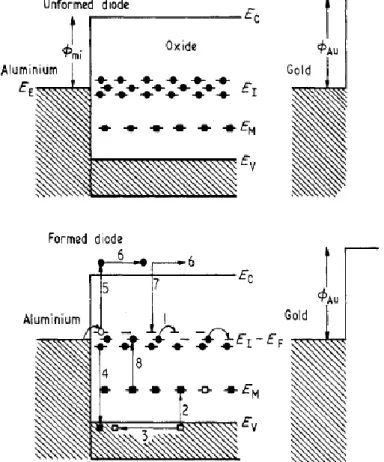
Resistive values, triggered by applying voltage/current bias or pulse to different resistance values; they were first discussed several decades ago. These properties include the forming process phenomena, which is an essential and irreversible change in conductivity induced by a high electric field (Fig. 1-4). After forming, negative resistance (NDR), as well as switching and memory phenomena, is observed. These properties are demonstrated in a wide range of semiconductor materials, including amorphous or microcrystalline binary insulators prepared under certain appropriate conditions with suitable thickness or fabrication process. The basic structure of RRAM is composed of a metal-insulator-metal (MIM) or metal insulator semiconductor (MIS) stacked capacitor. Systems which show NDR have the following performed behaviors: current-controlled (S-type) and voltage-controlled (N-type) types, which imply that resistance change is triggered by applying current or voltage bias, as shown in Figs. 1-7(a) and (b).
1.2.1 Unipolar operation
behaviors. Two main categories of electrical behaviors, namely, unipolar and bipolar operation, have been reported and investigated in recent years. Unipolar operation denotes that the applied voltage used to trigger the resistive switching is based on the same polarity of voltage bias, that is, both by positive or negative bias. A typical unipolar electrical curve is shown in Fig. 1-8. After the electroforming process, the state is then switched to LRS. When the positive bias is re-applied, the electrical properties follow Curve 2 with a larger conducting current than the unformed sample. Until the applied voltage reaches a certain voltage value, a sudden decrease in current value is observed, and then the state is switched to high resistance state (HRS). As the positive bias is applied again, the current values - which are about 1 or 2 orders lower than the low resistance state (LRS), but are still higher than the unformed sample - increase gradually. Continuous increase in the applied voltage to a certain voltage value (Curve 1) results in an abrupt increase in the current. At this moment, the state is switched back to LRS. Two different conducting current values can be used as two different resistance states, namely, HRS and LRS, which are fundamental to RRAM devices. The voltage values which the state changes from HRS to LRS and LRS to HRS are denoted as the set voltage (Vset) and the reset voltage (Vreset), respectively,
whereas the switch process is called the SET and the RESET process. In some reported studies, unipolar RS is also called as nonpolar RS.
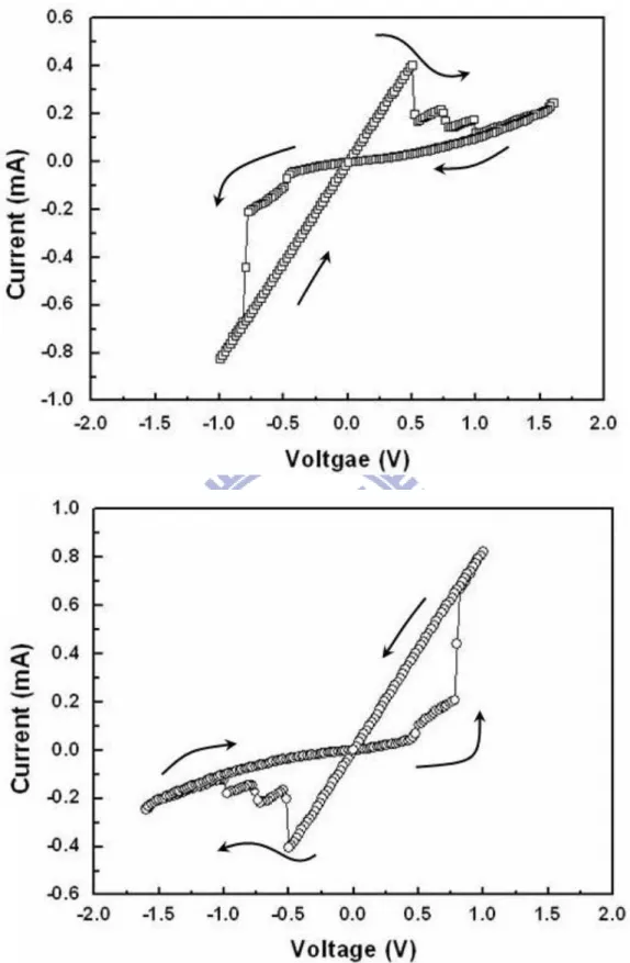
1.2.2 Bipolar operation
Bipolar RS depicts that the RS phenomenon is observed by applying a specific polarity of voltage or current bias to reach the LRS state, or back to the HRS state by applying another polarity of the voltage or current bias [Figs. 1-9 (a) and (b)]. Bipolar switching can be performed by the following two sweeping current loops: clockwise and counterclockwise current loops. The clockwise current loop indicates that a