行政院國家科學委員會專題研究計畫 成果報告
鎳陶瓷奈米複合材料之製作與特性的探討及其在高密度,高
深寬比之穿透晶片導線與微機電系統製作上之應用
計畫類別: 個別型計畫 計畫編號: NSC92-2215-E-009-043- 執行期間: 92 年 01 月 01 日至 92 年 07 月 31 日 執行單位: 國立交通大學電子工程學系 計畫主持人: 鄭裕庭 報告類型: 精簡報告 處理方式: 本計畫可公開查詢中 華 民 國 92 年 10 月 31 日
行政院國家科學委員會補助專題研究計畫
■成果報告
期中進度報告
鎳陶瓷奈米複合材料之製作與特性的探討及其在高密度,高深
寬比之穿透晶片導線與微機電系統製作上之應用
計畫類別:■ 個別型計畫
計畫編號:NSC
92-2215-E-009-043-執行期間: 92 年 1 月 1 日 至 92 年
7 月 31 日
計畫主持人:
國立交通大學電子工程系 鄭裕庭 助理教授
共同主持人:
計畫參與人員:
成果報告類型(依經費核定清單規定繳交):■精簡報告 □完整報告
本成果報告包括以下應繳交之附件:
□赴國外出差或研習心得報告一份
□赴大陸地區出差或研習心得報告一份
□出席國際學術會議心得報告及發表之論文各一份
□國際合作研究計畫國外研究報告書一份
處理方式:除產學合作研究計畫、提升產業技術及人才培育研究計畫、列管計畫及
下列情形者外,得立即公開查詢
□涉及專利或其他智慧財產權,□一年□二年後可公開查詢
執行單位:
國立交通大學電子工程系
中 華 民 國 92 年 10 月 31 日
鎳陶瓷奈米複合材料之合成與特性的探討及其在微機電系統製作上之應用 Fabrication and Characterization of Ni nanocomposites for MEMS Applications
計劃編號: 92-2215-E-009-043- 執行期間:92 年 1 月~92 年 7 月 計劃主持人:交通大學電子系 鄭裕庭 助理教授 e-mail:[email protected] 摘要 本計劃開發出以鎳陶瓷奈米複合材料為結 構主體之微機電系統元件製程技術,藉由第二 相之異質與本體結構的增益效應來達成提供可 調 變 之 薄 膜 性 質 , 以 nickel-cordierite and diamond 複合薄膜為例,本研究發現該奈米複合 材料皆具有低於傳統電鍍鎳之熱膨脹係數,利用 本製程技術將可成功製作出無殘純應力之鎳陶瓷 奈米微振動器。此外藉由微懸臂之共振頻率的量 測實驗,發現利用nickel-diamond 所製作出之懸 臂會因材料的楊氏系係數(Young’s Modulus)對密 度比之增加而提升其共振頻率,其中隨著嵌入於 鎳金屬膜之鑽石粉末增加,將可增益楊氏系係數 (Young’s Modulus)對密度比達 2.5 倍之多,非常適 合超高頻之微振盪器之製作。 ABSTRACT
In this report, we demonstrate the successful
device-level fabrication of microelectromehcanical systems (MEMS) using a
metal matrix nanocomposite material via a CMOS-compatible process. The discontinuous metal matrix nanocomposite (DMMN) is composed of an electrolytic (EL) or electroless (EN) plated nickel matrix, with nano cordierite (diameter » 100 nm ~ 5 mm) or diamond (diameter » 4 ~ 500 nm) embedded within. Through the addition of cordierite nanoparticles, the as-deposited EN-cordierite films show marked improvement in thermal compatibility with silicon (Si) substrate. By means of Fabry-Perot laser interferometry, the coefficient of thermal expansion (CTE) of EN-cordierite is measured to be 17.34 ppm/K, compared to 26.69 ppm/K for pure EN. On a similar note, it is also found that as the amount of incorporated diamond nanoparticles increases, the intrinsic tensile stress and temperature sensitivity of EL film is reduced proportionately. Furthermore, based on the resonant frequency measurements of micro-cantilever beams, the results verify that more nanodiamond incorporation into a Ni film can greatly improve the film mechanical properties. The E/ρ ratio of the Ni-diamond nanocomposite synthesized in a plating solution with 2.0g/L diamond powders is 2.5 times larger than that of a pure Ni.
I. INTRODUCTION
Silicon (Si) has been utilized extensively and almost exclusively as the structural material for planar, movable MEMS structures such as the
microresonator [1], microgyroscope [2], micromirror [3] and radio frequency (RF) microrelay [4]. As a research material, Si is extremely robust and versatile in terms of fabrication, and it has good mechanical properties such as Young’s modulus (~160 GPa), yield strength (~ 7GPa) and fatigue life. However, as MEMS transitions from being a promising academic research into budding commercial products, the use of Si has increasingly seen its limitations. One of the most fundamental shortcomings of Si lies in its inherent high processing temperature - as above-average quality polySi films are generally produced at or above 600°C. This requirement prohibits the concurrent, monolithic fabrication of CMOS circuits and polySi MEMS structures, which in turns gives rise to the need for modular post-CMOS MEMS-circuits integration.
On the other hand, metals, being good conductors, and capable of being processed via a huge repertoire of processing technologies at low cost, would also be good candidates as MEMS structural materials. Indeed, metal-based microstructures have been studied before the emergence of polysilicon, yet they suffered from mechanical deficiency such as aging and fatigue [5]. To overcome the challenges, previous studies have shown that the inclusion of second-phase particles in a ductile metal matrix can improve the mechanical strength through a composite effect [6,7]. Hence, an optimal solution would be the addition of nanoparticles into metal MEMS structures to potentially strengthen the material properties, with the added advantage of low temperature processing and feasibility for direct integration with microelectronics.
Nickel-nanocomposite is being explored as a potential material in the work that could be used in place of polySi in certain applications, such as microresonators, RF MEMS metal switches, optical micromirror arrays, and 3-D interconnects in the silicon substrate. One of the major advantages of using nickel-nanocomposites is their low deposition temperatures, which could be as low as 50°C. This is achieved by combining an electroless or electrolytic plating technique, and the modification of surface catalytic property to selectively produce film growth in targeted areas on the substrate. Furthermore, the film’s thermal and mechanical properties can be engineered according to the types, and amount, of nanoparticles used. We have previously discovered that the incorporation of cordierite nanoparticles in a blanket nickel film being capable of attenuating the effect of thermal mismatch between silicon substrate and EN (Electroless Nickle) film. This is achieved without
compromising the Young's modulus and electrical conductivity of the EN film [8]. The preliminary evidences also provide a plausible premise for us to hypothesize that, one may indeed increase the stiffness of the nickel film by embedding extremely hard and stiff nanoparticles, such as nanodiamond, in the metal matrix. In this report, we will further demonstrate the fabrication of microresonators via this technology with more material characterization results.
II. FABRICATION TECHNOLOGY
Figure 1 illustrates the fabrication of an EN-nanocomposite microresonator via a three-mask surface micromachining process. The process begins with the blanket deposition of a layer of low pressure chemical vapor deposited (LPCVD) silicon nitride (SiXNy) film (4000Å, at
835°C). The nitride serves as an insulation layer onto which a conductive, phosphorous-doped polysilicon layer (5000Å, at 610°C) is deposited via LPCVD, and subsequently patterned using photolithographic method to define the ground layer and electrical interconnects to the microresonators. The anchor region of the double-folded beams of the microresonator is next defined on a layer of sacrificial phosphosilicate glass (PSG) that is LPCVD deposited, and reactive-ion etched. Besides serving as a sacrificial layer, PSG also serves as a doping source (phosphorous) for the underlying polySi, and hence helps reduce the sheet resistance of the polySi further.
For EN-nanocomposite plating, a thin Cr/Cu primary seed layer (150Å/600Å) is next sputtered and lifted-off to define the plating region. Subsequent activation in PdCl solution ensues, before wafers are plated in the EN/EL or EN/EL(Electrolytic Nickel)-cordierite bath. During the activation process, Pd will form a catalytic layer on the Cu surface, which acts as nucleation sites for EN-composite to deposit. On the other hand, for EL-nanocomposite plating, a thin seed layer of Cr/Cu or Cr/Au (150Å/600Å) is blanket-sputtered after patterning the PSG. This is then followed by a photolithographic step to define the photoresist mold whereby EL-nanocomposite will selectively deposit later. For both EN- and EL-nanocomposite plating processes, a 1 mm film is selectively deposited at a rate of 2 mm/hour. The fabrication process terminates with the sacrificial-PSG removal in CMOS-grade HF, and upon final release in supercritical-CO2 for stiction elimination. The fabrication flow of MEMS device, cantilever beam, is shown in Fig.1.
Prior to the plating process, dry nanoparticles are dispersed in the plating bath by both mechanical stirring and sonication. The wafer is subsequently placed in a vertical fashion in the plating solution,
which continued to be stirred at 120 rpm (EN) and 250 rpm (EL). The bath temperatures are maintained at 70°C (EN) and 50°C (EL) for optimum mechanical performance. During the plating process, Ni2+ ions in the solution continue to be reduced at (in the case of EL) or near (by hypophosphate ions in the case of EN) the cathode (wafer), and precipitated to form a layer of nickel film on the cathode. Another event that occurs simultaneously is the arrival of the nanoparticles in the vicinity of the plated surface due to convective current. The existence of a boundary layer near the plated surface helps retard the velocity of these particles. In a stochastic fashion, some of the nanoparticles become momentarily adsorbed onto the surface, and subsequently encapsulated by the rapidly thickening nickel matrix around them. Using the DLVO theory of colloid stability [9,10] as an approximation tool, the amount of adsorbed nanoparticles can be adjusted via controlling the electrolyte (and organic) species, electrolyte concentration, size/shape/concentration of nanoparticles, speed of agitation as well as temperature. Thus, in the experiment, cantilever beams made of pure Ni and Ni-diamond nanocomposite with four different concentrations of diamond powder, which are 0.5g/L, 1.0g/L, 1.5g/L and 2.0g/L nanodiamond (0.5µm in diameter)/Ni in well mixed solutions, respectively, are designed and used for the characterization of the composite materials and the verification of the fabrication process.
III. EXPERIMENTAL RESULTS
A) NICKEL-CORDIERITE : DEVICE FABRICATION & CHARACTERIZATION
Figures 2 (a)-(b) and 2 (c) show the scanning electron micrograph (SEM) and electron dispersive spectrum (EDS) of a 5 µm thick EN-cordierite film after 30 minutes of deposition, respectively. The SEM shows the extent of large spherical cordierite particles of 4 ~ 5 mm being embedded in the nickel matrix. There is no visible interfacial defects (cracks, delaminations) from the appearance of these particles. While not optically visible, the existence of smaller, sub-micron nanoparticles is confirmed by the EDS, as evident from the elemental peaks of Al, Mg, Si and O, which are the constituent elements
of the cordierite particles (2MgO•2Al2O3•5SiO2). In addition to the film
cross section, we have also investigated the effect of agitation on the deposition profile of EN film. As shown in Figure 3 (a) through (c), as the rate of agitation increases from 0 rpm to 80 rpm and then to 120 rpm, non-specific nucleation (i.e. nucleation outside the catalytically treated area) of EN becomes progressively less prominent, and is eventually eliminated. Figure 3 (d) shows a
pre-released microresonator fabricated at 70°C and 120 rpm.
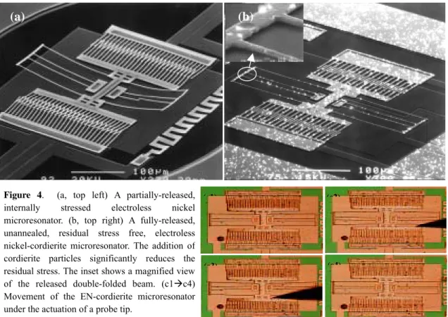
Figure 4 (a) and (b) juxtaposes a fabricated EN and EN-cordierite microresonators alongside each other. Figure 4 (a) shows a partially-released EN microresonator deforming out-of-plane due to tensile stress build-up during post-deposition cooling. The EN-cordierite microresonator in Figure 4 (b) is plated in a plating bath that contains 4 g/L of well-dispersed cordierite micro- and nano-particles. As shown in Figure 4 (b), no out-of-plane deformation is observed for a fully-released EN-cordierite microresonator. This qualitatively demonstrates that the addition of an adequate volume fraction of cordierite particles in the EN matrix is capable of evening out the residual stress gradient within the metal matrix, and hence negating the effect of residual stress substantially. Figure 4 (c1-c4) shows the movement of the microresonator under the actuation of a probe. Through the use of a FLEXUS FLX-2320™ laser interferometer, the CTE of the EN-cordierite is measured to be 17.34 ppm/K, vis-à-vis EN at 26.69 ppm/K and cordierite at 2.1 ppm/K. This shows a marked improvement in terms of thermal compatibility between the EN-cordierite film and the underlying Si substrate. (A). MEMS devices and mechanical properties
B) NICKEL-DIAMOND: DEVICE FABRICATION & CHARACTERIZATION
Based on the material characterization results obtained from EN-cordierite composite film, we firstly hypothesize that, due to the extreme hardness, stiffness and temperature-resistance of diamond particles, the incorporation of nanodiamond particles may enhance the overall stiffness of nickel film, as well as its temperature-resistance. Figure 5 shows that the as-measured thermal residual stress decreases as the EL and EL-diamond film temperatures is gradually raised from 40°C to 200°C. Although both EL and EL-diamond films stress-relieve with increasing temperature, diamond particle reduces the thermal residual stress of EL film, as evident from the smaller stress-temperature gradient, and hence smaller sensitivity towards temperature change. This evidence indicates that the temperature-resistance of nickel can be improved by the addition of diamonds. Hence, EL-diamond nanocomposite could be an ideal material for MEMS that requires structural and mechanical integrity at elevated temperature. Figure 6 shows a microresonator made of EL-diamond for future performance testing.
Figure 7 shows a SEM photograph of the fabricated cantilever beam array. The beams are all 50µm in width. Each of them has different length. They are 150, 250, 350 and 450µm, respectively.
According to the beam theory, the resonant frequency of a cantilever beam is proportional to the E/ρ ratio of the structural material as described in the formula: ρ E h l = 0.1615 2 (1) f
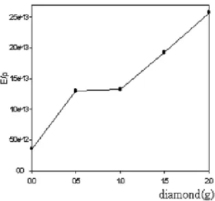
where l is the beam length, h is the thickness, ρ is the density and E is the Young’s modulus. Therefore, via the measurement of the resonant frequency of the cantilever beam which is 50µm wide, 250µm long and 5µm thick, we find the linear relationship between E/ρ ratio and the nanodiamond concentration in the plating solution as shown in Fig.8. It indicates that the E/ρ ratio can be enhanced with the increase of naondiamond concentration. In addition, the E/ρ ratio of the Ni-diamond cantilever plated in a bath with the concentration of 2.0g/L diamond nanopowders is 2.5 times larger than that of a pure Ni cantilever. The result infers more nanodiamond incorporation into the Ni film indeed greatly improve the film mechanical properties.
IV. SUMMARY
We have demonstrated a novel, CMOS-compatible and low cost process for possible wafer-level, stress-free nanocomposite fabrication of MEMS devices. CTE and residual stress reduction and E/ρ enhancement of nickel films have been shown via the co-deposition of cordierite and diamond nanoparticles. Both electroless nickel and electrolytic nickel deposition processes have been used to construct the structural layer in a surface-micromachining process using silicon dioxide as the sacrificial layer. Experimental results show that fixed-fixed microbeams as well as comb-shape microresonators can be fabricated with the nanocomposite materials and further experimental results are required to characterize the device performance.
REFERENCES
[1] W. C. Tang, T.-C.H. Nguyen, R. T. Howe, “Laterally Driven Polysilicon Resonant Microstructures”, Proc. IEEE Workshop on Microelectromechanical Systems, pp. 53-59, Salt Lake City, UT, USA, 1989.
[2] M.W. Putty, and K. Najafi, “A Micromachined Vibrating Ring Gyroscope”, Invited Paper, Technical Digest, Solid-State Sensors and Actuators Workshop, pp. 213-220, Hilton Head, SC, June 1994.
[3] G. D. J. Su, MEMS High-Quality Micromirrors For Optical Interconnect And Optical Pick-Up
Heads, PhD Thesis, UCLA, CA, USA, 2001.
[4] J. J. Yao, “RF MEMS From A Device Perspective”, J. Micromech. Microeng., v10, pp. R9-38, 2000.
[5] H. C. Nathanson, R. A. Wickstrom, “A Resonant-Gate Silicon Surface Transistor With High-Q Band-Pass Properties”, App. Phys. Letters, v. 7, No. 4, pp. 84-86, 15 Aug. 1965.
[6] R. Warren, Ceramic-Matrix Composites, Chapman and Hall Inc., NY, 1990.
[7] D. Hull, An Introduction to Composite Materials, Cambridge University Press, Cambridge, 1981.
[8] K. S. Teh, Y. T. Cheng and C. Sambucetti, “Selective Plating of Nickel Composite Films for MEMS Applications”, Proc. 15th Annual Int. Conference on Micro Electro Mechanical Systems, pp. 384-387, Las Vegas, NV, USA, 2002.
[9] B. V. Derjaguin, L. Landau, Acta Physicochim. Urss, v. 14, pp. 633, 1941.
[10] E. J. W. Vervey, J. T. G. Overbeek, Theory Of The Stability Of Lyophobic Colloids, Elsevier, Amsterdam, 1948.
LSN Polysilicon Cr/Cu Nickel plating solution with cordierite micro/nano-particles well-dispersed. Temp = 70C Thermometer Magnetic stirrer Nickel-Cordierite (a) (c) (e) (f) (d) (b) PSG Ni2+ Ni2+ Ni2+ Ni2+ Ni2+
Figure 1. The 3-mask fabrication process begins with (a) the deposition of 4000Å of silicon nitride (SixNy)
and 5000Å of phosphorous-doped polysilicon on top of a p-type Si wafer. (b) Polysilicon is then reactive-ion etched (RIE) by Cl2 to define the ground plane and interconnects. 2µm of LPCVD phosphosilicate glass
(PSG) is next deposited as sacrificial layer. This is followed by (c) patterning the PSG for the anchor area, and patterning sputtered Cr/Cu (150Å/600Å) with a lift-off process. (d) The processed wafer is then seeded in Pd solution, immersed in a nickel-composite plating solution to selectively grow nickel-composite thin film. During the film growth process, Ni2+ ions are reduced by the hypophosphite ions to produce nickel
film, which embed nanoparticles simultaneously, yielding the structure in (e). Hydrogen gas is also evolved during this process. (f) 49% HF solution is used to release the structure by etching away the sacrificial PSG layer prior to a supercritical CO2 release.
Cordierite
Cordierite
Figure 2. (a, left) Oblique view and (b, center) cross-sectional view of a 5µm EN-cordierite thin film
grown on a silicon substrate. (c, right) EDS confirms the existence of sub-micron cordierite particles embedded within the EN matrix. It also indirectly implies that particles of various sizes are well-distributed within the matrix.
Non-specific (b) Non-specific (c)
(a)
Figure 3. The deposition profile of EN on the microresonator interdigitated fingers under various agitation magnitudes: (a) 0 rpm, (b) 80 rpm, and (c) 120 rpm (the white fringes around the fingers are due to electron charging effect on the sacrificial PSG). As shown, non-specific nucleation of EN can be reduced and eliminated through an optimal amount of agitation. (d) A completed microresonator fabricated at 120 rpm agitation rate. Shuttle Mass Anchor Double Folded Beam Interdigitated fingers (d)
Figure 4. (a, top left) A partially-released, internally stressed electroless nickel microresonator. (b, top right) A fully-released, unannealed, residual stress free, electroless nickel-cordierite microresonator. The addition of cordierite particles significantly reduces the residual stress. The inset shows a magnified view of the released double-folded beam. (c1Æc4) Movement of the EN-cordierite microresonator under the actuation of a probe tip.
(b) (a) (c4) (c3) (c2) (c1) -4 00 -3 00 -2 00 -1 00 0 100 200 300 400 0 50 100 150 200 250
Graph of Film Stress vs. Temperature
1g/L
No Diamond
Te mpe ratur e [C]
he composite effect of diamond nanoparticle manifests itself via film stress r
Figure 5. T eduction. When temperature
increases from 40°C to 200°C, EL-diamond shows less sensitivity to the temperature compared to EL film, as shown by the smaller gradient of the curve.
Figure 6. (a, left) An EL-diamond microresonator. (b, right) A dark field optical micrograph of the
Figure 7. SEM micrograph of the fabricated EL Ni-diamond composite cantilever beams. The array of beams is 50µm in width, and their lengths are 150, 250, 350 and 450µm, respectively.
Figure 8. The E/ρ ratio of Ni-diamond composite versus the concentration of the well dispersed diamond particles in the plating solution (E: Young’s modulus, ρ: film density).