國
立
交
通
大
學
電信工程學系
碩
士
論
文
應用於超寬頻系統之電流再利用低雜訊放大器、
9-26GHz 寬頻互補式電晶體低雜訊放大器
之設計與研究
Design of Current-Reused LNA for UWB,
9-26GHZ Wideband CMOS LNA
研 究 生:林宗廷
指導教授:周復芳 博士
應用於超寬頻系統之電流再利用低雜訊放大器、
9-26GHz 超寬頻互補式電晶體低雜訊放大器
之設計與研究
Design of Current-Reused LNA for UWB,
9-26GHZ Wideband CMOS LNA
研 究 生:林宗廷 Student:Tsung-Ting Lin
指導教授:周復芳 Advisor:Dr. Christan F. Jou
國 立 交 通 大 學
電 信 工 程 學 系 碩 士 班
碩 士 論 文
A Thesis
Submitted to Department of Communication Engineering
College of Electrical and Computer Engineering
National Chiao Tung University
in Partial Fulfillment of the Requirements
for the Degree of Master of Science
應用於超寬頻系統之電流再利用低雜訊放大器、
9-26GHz 寬頻互補式電晶體低雜訊放大器
之設計與研究
研究生:林宗廷 指導教授:周復芳 博士
國立交通大學電信工程學系碩士班
摘 要
本論文的第一部份提出一超寬頻低雜訊放大器。此電路輸入阻抗之匹配是利用電流再利 用應用於 LC Ladder 使得此架構適合低電壓使用,然而在利用電流再利用之技術來放大 射頻訊號。因此超寬頻低雜訊放大器能夠同時達到輸入端寬頻匹配與高增益。模擬結 果:-10dB 之輸入與輸出端反射損耗、3.3dB 之最小雜訊指數、14.3dB 之最高增益並消耗 17.75mW 之功率。 第二部份針對不同於 3.1-10.6GHz 的低雜訊放大器設計提出一利用 0.18 製程所達到 9-26GHz 之低雜訊放大器。此電路設計是期望能利用 L 和 R-C 匹配方式,來達到寛頻 及相對低的雜訊指數。模擬結果: -10dB 之輸入與輸出端反射損耗、低雜訊、高增益於 不同偏壓情況下。Design of Current-Reused LNA for UWB,
9-26GHZ Wideband CMOS LNA
Student: Tsung-Ting Lin Advisor: Dr. Christan F. Jou
Department of Communication Engineering
Nation Chiao Tung University
ABSTRACT
In the first part of this thesis, an ultra-wideband (UWB) LNA is proposed. The
input matching of this circuit used a LC Ladder with current-reused so that this
topology is suitable for low voltage. Using current-reused to amplify RF signal.
Therefore, the proposed LNA can simultaneously achieve input impedance
matching and high gain. The simulated results:-10dB input and output return
loss, minimum noise figure of 3.3dB, and maximum gain of 14.3dB from
17.75mW.
In the second part, a 9-26GHz LNA using 0.18um technology different from
3.1-10.6 GHz (In general, the 0.18um CMOS LNA usually be designed for
3−10GHz operating range.) is proposed. The design of this circuit used L and
R-C matching to achieve wideband and low noise figure. The simulated
results:-10dB input and output return loss, low noise figure, and high gain at
different bias voltage.
致謝
能夠完成碩士這兩年的學業,首先我要先感謝我的指導老師周復芳博士,再這兩年的期 間總是能適時的給我關心以及指導,不僅讓我在射頻積體電路設計的領域上有很好的基 礎也讓我的心態與態度都有所成長。也感謝電子工程學系胡樹一教授給我一個機會能開 始 接 觸 如 何 設 計 低 雜 訊 放 大 器 以 及 論 文 口 試 委 員 郭 建 男 授的不吝指導。 我也要感謝這兩年陪伴在求學生涯的實驗室同伴們。感謝匯儀、俊偉、宜星、智鵬、沛 遠 、 志 豪 、 廉 昇 、 昱 舜 、 智 遠 、 昭 竹 學 長 們 , 還 有 我 的 同 學 子 哲 、 昭 維 、 玠煌,奕霖平常的教導以及可以一起打球真的很快樂! 最後我要感謝我的父母、姊姊、以及我的最佳好友暐程、致遠、棋浩、慧慈,謝謝你們 當 我 在 最 需 要 你 的 的 時 候 都 能 適 時 的 出 現 給 我 力 量 , 讓 我 能 順 利 的 完 成 兩 年的碩士學位。 Nino @ 2009 年 新竹 夏Contents
Chinese Abstract……….Ⅰ
English Abstract………..Ⅱ
Acknowledgment………Ⅲ
Contents………...Ⅳ
List of Tables………...Ⅴ
List of Figures……….Ⅵ
Chapter 1 Introduction………..………...- 1 -
1.1
Background and motivation………-1-
1.2
Thesis organization……….-2-
Chapter 2 Design of Current-Reused LNA for UWB…………...- 4-
2.1
Introduction………-4-
2.2
Numerous topology of wideband LNA………..-4-
2.3
Conventional current-reused amplifier………...-8-
2.4
Architecture………..-10-
2.5
Design Considerations………..-11-
2.5.1 Input matching analysis……….-11-
2.5.2 Gain analysis……….-16-
2.6
Chip implementation and simulated results……….-16-
2.6.1 Layout considerations………-16-
Chapter 3 9−26GHz Wideband CMOS LNA
Design…………..-25-3.1
Introduction………..-25-
3.2
The principles of narrowband LNA……….-26-
3.3
Architecture………..-27-
3.4
Design Considerations………..-28-
3.5
Chip implementation and simulated results………..-31-
3.5.1 When
Vg =0.8Vand
Vd =2.0V………-32-
3.5.2 When
Vg =0.8Vand
Vd =1.4V………-38-
Chapter 4 Conclusion and Future
Work………..…-44-4.1 Conclusion and Future Work………-44-
References……….-45-
List of Tables
Table 2.1 Performance summary of the proposed LNA………-23-
Table 2.2 Comparison of UWB LNA………...-24-
Table.3.1 The used frequency band of the applications……….-26-
Table3.2 Performance summary of the proposed LNA……….-37-
List of Figures
Fig.1.1 DS-UWB spectrum allocation……….-1-
Fig.1.2 MB-OFDM UWB spectrum allocation……….……...-2-
Fig.2.1 (a) The transformer feedback amplifier………...-5-
Fig.2.1 (b) Resistive shunt-feedback amplifier………-5-
Fig.2.1 (c) The common-gate amplifier………...-6-
Fig.2.1 (d) The distributed amplifier………...-7-
Fig.2.2 The LC ladder with current-reused topology………...…………...-8-
Fig.2.3 The current-reused amplifier topology………-9-
Fig.2.4 Schematic of the proposed UWB LNA………..……-10-
Fig.2.5 Fourth-order bandpass filter used for impedance matching……….……..-11-
Fig.2.6 Input impedance of the bandpass filter versus frequency……….……….-11-
Fig.2.7 The overall input matching small signal equivalent circuit……….….…….-12-
Fig.2.8 Input small signal equivalent circuit at high frequency………..……...-13-
Fig.2.9 Input small signal equivalent circuit at low frequency……….….…-13-
Fig.2.10 Simulated input reflection coefficients………....-15-
Fig.2.11 Simulated input reflection coefficients………-15-
Fig.2.12 Chip layout of the UWB LNA……….………...….-17-
Fig.2.13 Simulated result of S11……….……….………..-18-
Fig.2.14 Simulated result of S22………...………….………-18-
Fig.2.15 Simulated result of S21……….………….………..-19-
Fig.2.16 Simulated result of S12……….………...-19-
Fig.2.17 Simulated result of NF……….………....-20-
Fig.2.18 Simulated results of IIP3 at (a) 3.1GHz……….…..………....-20-
Fig.2.18 Simulated results of IIP3 at (b) 6.8GHz. (c) 10.6GHz……….…………-21-
Fig.2.19 Simulated results of P1dB at (a) 3.1GHz. (b) 6.8GHz. (c) 10.6GHz…………...-22-
Fig.3.1 (a) The input part of a typical narrowband LNA………...………-26-
Fig.3.1 (b) The small signal equivalent circuit……….…………..-26-
Fig.3.2 The schematic of the proposed LNA……….……...……...…..-27-
Fig.3.3 The overall input matching small signal equivalent circuit……….………..…-28-
Fig.3.4 Input small signal equivalent circuit at high frequency………….………….……...-28-
Fig.3.5 Input small signal equivalent circuit at low frequency……….……….-29-
Fig.3.6 Simulated input reflection coefficients………..-30-
Fig.3.7 Simulated output reflection coefficients………-30- Ⅶ
Fig.3.8 The power line of the proposed LNA………....-31-
Fig.3.9 Chip layout of the UWB LNA………..……….-32-
Fig.3.10 Simulated result of S11……….…………...-33-
Fig.3.11 Simulated result of S22……….……...-33-
Fig.3.12 Simulated result of S21……….…..…….-34-
Fig.3.13 Simulated result of S12……….……...…-34-
Fig.3.14 Simulated result of NF……….……-35-
Fig.3.15 Simulated results of IIP3 at (a) 9 GHz……….….……...-35-
Fig.3.15 Simulated results of IIP3 at (b) 18 GHz (c) 26 GHz………..……..……-36-
Fig.3.16 Simulated result of Stability……….…………-37-
Fig.3.17 Simulated result of S11……….……...-38-
Fig.3.18 Simulated result of S22……….…..….-39-
Fig.3.19 Simulated result of S21……….……...-39-
Fig.3.20 Simulated result of S12………-40-
Fig.3.21 Simulated result of NF……….…………-40-
Fig.3.22 Simulated results of IIP3 at (a) 9 GHz (b) 18 GHz……….…………-41-
Fig.3.22 Simulated results of IIP3 at (c) 26 GHz………..………-42-
Chapter 1
Introduction
1.1 Background and motivation
The Federal Communications Commission (FCC) authorize the unlicensed use of ultra-wideband(UWB) in 3.1-10.6 GHz in February 14 2002[1]. UWB is a technology that can be used at very low energy levels for transmitting information spread over a large bandwidth (>500 MHz). Beside, UWB communications transmit in a way that doesn't interfere largely with other more traditional narrow band and continuous carrier wave uses in the same frequency band. Direct sequence code division multiple access (DS-CDMA) and multi-band orthogonal frequency division multiple access (MB-OFDM) are two mainly modulation technologies for UWB communications. The DS-CDMA UWB supports two independent operated bands. The lower band occupies the spectrum from 3.1-5.15 GHz and the upper band occupies the spectrum from 5.825-9.7 GHz as shown in Fig.1.1
Fig.1.1 DS-UWB spectrum allocation
The MB-OFDM UWB, the 7500-MHz bandwidth is divided into 5 major Band Groups which are in turn sub-divided into 14 bands in total and each band is 528MHz bandwidth and each band includes 128 sub-channels, sub-channel is 4.125 MHz as shown in Fig.1.2.
Fig.1.2 MB-OFDM UWB spectrum allocation
The low-noise amplifier (LNA) is a key component in the front-end of a radio receiver circuit. It is located after the antenna, so that losses in the feedline become less critical. The overall noise figure of the receiver front-end is dominated by the first few stages. Using an LNA, the noise of all the subsequent stages is reduced by the gain of the LNA, while the noise of the LNA itself is injected directly into the received signal. Thus, it is necessary for an LNA to be low noise and high gain.
1.2 Thesis organization
This thesis will discuss about the two kinds of circuit and implementation for ultra-wideband applications. The contents consist of two major topics:” Design of current-reused LNA for UWB ” and “ 9−26GHz Wideband CMOS LNA Design ” , respectively in chapter 2 and chapter 3. In these chapters, we will propose the architecture and explain the circuit. The circuit principles, design consideration and Layout consideration will be analyzed. In chapter 2, we discuss several researches recently. By improving their drawback, we proposed current-reused amplifier which stacking NMOS and PMOS. The input impedance can be achieved 50 over the frequency band of interest and the gain will not reduce due to the enhancement of transconductance. The details will be explained in chapter2.
In chapter 3. Base on the technology of the narrowband LNA, we use the LC matching and five-stage common source cascade architecture to achieve a wideband 9 – 26 GHz and low noise circuit. The details will be explained in chapter 3.
Chapter 2
Design of Current-Reused LNA for UWB
2.1 Introduction
The ultra-wideband (UWB) system is a high data rate , low power consumption and for a short range wireless personal area network technology [2][3]. Because it can handle the requirement of high transmission speed for the multimedia material ( for example phantom and sound ) , it becomes more and more popular for wireless system. The FCC has defined 7500 MHz bandwidth in 3.1 - 10.6 GHz frequency range ( lower band : 3.1 – 5 GHz ; upper band : 6 – 10.6 GHz ) for the UWB standard IEEE 802.15.3a.
One of the challenges is to design the front-end LNA. Because it is the first block in the radio receiver, its performance will affect the sensitivity of the overall system. Thus, it is necessary for an LNA to boost the desired signal power while adding as little noise and distortion as possible so that the retrieval of this signal is possible in the later stages in the system.
2.2 Numerous topology of wideband LNA
Because of the input matching can directly affect the noise performance of an LNA. Thus, there are some researches that can provide 50 input impedance over a wide bandwidth will be discussed as follow.
Fig.2.1 (a) The transformer feedback amplifier
(a) The transformer feedback amplifier[4][5]
The transformer feedback topology has good input matching entire frequency band of interest. There is no input matching devices in the input gate of the purpose circuit, so that the LNA can achieve lower NF. However, the transformer silicon set up is very sensitive to the technology dispersions thus strengthening the design hardness.
(b) Resistive shunt-feedback amplifier[6]
The resistive shunt-feedback topology could have better bandwidth than conventional low noise amplifier, but it has limited input matching or NF and vice versa. In other words, the resistive shunt-feedback amplifier exhibits trades off in terms of bandwidth, input matching and NF. Indeed, its lower voltage gain will cause the noise of next stage won’t be suppressed.
Fig.2.1 (c) The common-gate amplifier
(c) Common-Gate amplifier[7]
The input impedance is approximately as
gs m in jwC g Z
1 . In the low frequency, the input
impedance is approximately as
m in
g
Z 1 . It is easy to be matched to the 50 . However,
with the increasing of the operating frequency, the parasitic transistor capacitance (C ) gs degrades the amplifier performance in the high frequency. In addition, its noise is also larger than that of the other topologies.
Fig.2.1 (d) The distributed amplifier
(d) Distributed amplifier[8]
The distributed amplifier that can provide wide bandwidth and relatively flat gain over entire frequency band of interest. However, due to multiple transistor stages and much inductors are used so that the drawback is large power consumption and occupies large die size, respectively. In one word, it will make them unsuitable for integration.
Here, we proposed a LC ladder with current-reused topology for input matching as shown in Fig.2.2. To combine a NMOS and a PMOS transistor using the same supply voltage allows LC ladder technology to be low voltage compatible[9].
Fig.2.2 The LC ladder with current-reused topology
2.3 Conventional current-reused amplifier
Fig.2.3 shows the topology of current-reused amplifier. The current reused configuration can be considered as two-stage casade amplifier [10] [11], where the first stage M1 and the second stage M2 are two common-source amplifiers. The function of L1 and C1 is to perform a series-resonant with C of gs M for a low impedance path, and the impedance of 3
2
L is quite large to provide a high impedance path to block RF signal. Consequently, the RF signal can be amplified twice by this co-current structure. Because the resonate circuit
composed of L1 and C1 presents a narrowband characteristic, the current reused topology is designed to boost the gain at upper end of the required band. R1 and L is used to 3
compensate the high gain roll-off of the circuit. Due to the increased impedance of the L1 and C1 path, the function of current reused amplification is degraded at lower end of the designed band. However, by using LC ladder at input with current reused topology, an overall wideband flat-gain performance can be achieve.
2.4 Architecture
The proposed UWB LNA as shown in Fig.2.4 employs three stages. This circuit is designed to require three bias voltage sources of 1.0V (V ), 0.7V (dd V ) and 1.2V (g Vbias). The first input stage including LC ladder and M1p, M1n is current-reused configuration. It can provide wideband matching. The second stage M2 and the third stage M3 are current-reused configuration, too. A large resistor RL (5K ) is employed in bias circuit to isolate noise of voltage source from internal circuit. The function of C in input stage is to make the gate g wideband flat-gain performance can be achieve.
2.5 Design Considerations
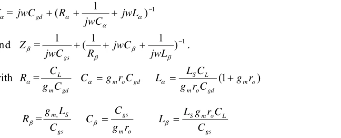
2.5.1 Input matching analysis
The proposed LNA use a fourth-order bandpass ladder filter to match 50 . The fourth-order bandpass ladder filter is shown in Fig.2.5[12].
Fig.2.5 Fourth-order bandpass filter used for impedance matching
From the results of recent research, we can find that the input impedance of the fourth-order bandpass ladder filter across the overall passband from WL to W is equal to a constant U resistance R as shown in Fig.2.6.
By means of a first approximation of the upper frequency (W ) and the lower frequency (U WL) of this LC ladder filter is given by:
1 1 RC WU and 1 2 1 L R RC WL . Obviously, the LC
ladder filter can provide a real impedance over a frequency band of interest. Because of the Fig.2.5 shows, the equivalent circuit of the inductively degenerated transistor in Fig.2.5 looks like the right part of the bandpass filter. Therefore the overall input matching small signal equivalent circuit is shown in Fig.2.7.
Fig.2.7. The overall input matching small signal equivalent circuit
According to the novel wideband feedback mechanism proposed by [13].CL and RL are the parasitic capacitance and resistance which is contributed from the next stage. The capacitor
L
C dominates at low frequency and the resistor RL dominates at high frequency. The LNA input equivalent circuit at high frequency is shown in Fig.2.8.
Fig.2.8 Input small signal equivalent circuit at high frequency
While we assume that WLS,tot<<
tot gs WC ,
1
,WLS,tot<<R and we can find the input L impedance can be expression as following equation :
g in R jwC jwL Z ( // 1 ) 1 1 //Z (2-1) G where ( 1 ) [1 (1 ) 1] , , , , , , , 2 mtot L tot gs tot gd tot gs tot m tot S tot gs G g R C C C g L jwC jwL Z (2-2) tot S L O O jwL R r r , .
The LNA input equivalent circuit at low frequency is shown in Fig.2.9. In order to analysis the input impedance, we apart this circuit into two branches. Therefore, we can find the input
impedance is ( 1 ) 1 1 jwC jwL Zin //Z . (2-3) G whereZ =G jwL2+ 1 1 Z Y . (2-4)
Y is the impedance looking into the Cgd,tot and Z is the impedance looking into the
tot gs
C , . While we assume that the current flow through the capacitor Cgd,tot and Cgs,tot is smaller than the current source gm,totvgs. Thus
Y = , ( 1 )1 jwL jwC R jwCgdtot (2-5) and Z = 1 , ) 1 1 ( 1 jwL jwC R jwCgstot . (2-6) with R = tot gd tot m L C g C , , tot gd o tot m rC g C , , (1 , ) , , , o tot m tot gd o tot m L tot S r g C r g C L L (2-7) R = tot gs tot S tot m C L g , , , o tot m tot gs r g C C , , tot gs L o tot m tot S C C r g L L , , , (2-8)
Therefore, when the values of the inductors are designed properly, the input impedance will approach the 50 .
Fig.2.10 Simulated input reflection coefficients
Fig.2.11 Simulated input reflection coefficients
Fig.2.10 and Fig2.11 shows the simulated input reflection coefficients (S11) and the simulated output reflection coefficients (S22), respectively. As can be seen, the curve is near by the center of the Smith chart when frequency increases from 3.1GHz to 10.6GHz. In other words, this design can achieve wideband input matching successfully.
2.5.2 Gain analysis
Because of the current-reused configuration, the stacking NMOS and PMOS increase transconductance from g to approximately 2m g .In addition, by using m L4 and C2 is to perform a series-resonant with C of gs M4 for a low impedance path, and the impedance of
3
L is quite large to provide a high impedance path to block RF signal. Consequently, the RF
signal can be amplified twice by two current-reused configuration, respectively.
2.6 Chip implementation and simulated result
2.6.1 Layout considerations
The chip layout of the proposed LNA is shown in Fig.2.12, The skill of layout is very important for radio frequency circuit design, because high frequency will make more coupling and parasitic effects occur to influence performances. To get the high speed that the 0.18 m gate length was chosen. All elements with guard-rings can prevent noise and interference from substrate. Because the RF pad has parasitic capacitance that will degraded the RF signal, the RF pad with its size is 50 × 50 2
m
will be used. The smaller pad size can lead to a smaller parasitic capacitance. The bypass capacitors are used between each voltage source node and ground node to ensure voltage working like ground in AC and filter out noise. All connection wires are simulated by ADS momentum to extract parasitical effect.
Fig.2.12 Chip layout of the UWB LNA.
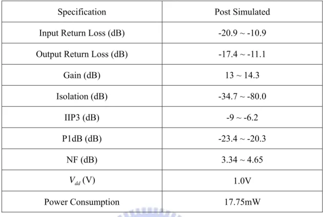
2.6.2 Simulated result
The chip size of the proposed LNA is 0.9690.895 2
mm and it is fabricated using TSMC
0.18 m mixed-signal/RF CMOS 1P6M technology. The total consumption is 17.758mW with bias voltage source of 1.0V and 1.2V. The simulated result of the input return loss (S11) and the output return loss (S22) in Fig2.13 and Fig2.14 is lower than -10 dB, respectively. The gain (S21) in Fig2.15 is 13dB~14.3dB over 3.1 ~10.6 GHz. The noise figure (NF) performance is shown in Fig.2.17. The simulated NF has maximum 4.65dB and minimum 3.34dB. The simulated input-referred third-order intercept point (IIP3) at three frequency points are shown in Fig.2.18 (a) ~ (c). The simulated IIP3 shows -9dB at 3.1GHz, -7dB at 6.8GHz, -6.2dB at 10.6GHz. The simulated input-referred 1dB compression point (P1dB) are
shown in Fig.2.19 (a) ~ (c). The simulated P1dB shows -23.4dB at 3.1GHz, -21.2dB at 6.8GHz, -20.3dB at 10.6GHz. The performance summary is listed in table 2.1. The performances of the proposed UWB LNA are compared with other works for UWB band listed in Table2.2.
-18-
Fig.2.15 Simulated result of S21
Fig.2.17 Simulated result of NF
(b)
(c)
(a)
(b)
(c)
Specification Post Simulated Input Return Loss (dB) -20.9 ~ -10.9
Output Return Loss (dB) -17.4 ~ -11.1
Gain (dB) 13 ~ 14.3 Isolation (dB) -34.7 ~ -80.0 IIP3 (dB) -9 ~ -6.2 P1dB (dB) -23.4 ~ -20.3 NF (dB) 3.34 ~ 4.65 dd V (V) 1.0V Power Consumption 17.75mW
Table 2.2 Comparison of UWB LNA Ref. Process BW (GHz) S11 (dB) S22 (dB) Gain ave.(dB) NF (dB) IIP3 Power (mW) This work (Sim.) 0.18um CMOS 3.1~10.6 <-10.9 <-11.1 13.5 3.3~4.7 -9.0 17.5 [8] 2004 (Sim.) 0.18um CMOS 3.1~10.6 <-10 <-9 18 5~7 N/A 54 [16] 2005 (Meas.) 0.18um CMOS 3.1~10.6 <-11 <-14 8.85 4.5~5.1 -6.2* 20 [17] 2007 (Meas.) 0.18um CMOS 3.1~10.6 <-9.7 <-8.4 11.4 4.12~5.16 0.72# 22.7 [18] 2008 (Meas.) 0.13um CMOS 3.1~10.6 <-17.5 <-14.4 7.92 2.5~4.56 -4* 10.68 [19] 2006 (Meas.) 0.13um CMOS 3.1~10.6 <-9.5 N/A 9.4 3.6~4.95 -7.2* 19
Chapter 3
9−26GHz Wideband CMOS LNA Design
3.1 Introduction
Square Kilometer Array (SKA) is one the most advanced radio telescope technology. Its observation and operation frequencies are 100MHz - 25GHz. The Square Kilometre Array (SKA) is a radio telescope in development which will have a total collecting area of approximately one square kilometre. It will operate over a wide range of frequencies and its size will make it 50 times more sensitive than any other radio instrument. By utilizing advanced processing technology it will be able to survey the sky more than ten thousand times faster than ever before.In the outer space communication aspect, in NASA Space Communication and Navigation Architecture Recommendations for in 2005-2030 of Space Communication Architecture Working Group (SCAWG) has the very clear introduction to the future outer space communication construction[14]. It divides SCA into approximately four regions : earth, moon, mars vicinity and deep space. And it uses the frequency of UHF, S, L, K, Ku and Ka frequency bands. For example, Ground-based Earth Element to Near-Earth Relay Element is use 13 ~ 15 GHz and Launch Vehicles、Earth Orbital User、Lunar Surface and Orbital User is use 22 ~ 27 GHz. Therefore, that is the reason we chose 9 – 25 GHz frequency band to design LNA. The table.3.1 shows the used frequency band of the applications.
Application Frequency Band
Astronomy SKA 100MHz – 25GHz
Military EW / ECM 9 – 26 GHz
Satellite Communication Lower Ka-band 17.7 – 21.2 GHz Space Communication Ground to Space 13 – 15 GHz Space Communication Space to space 22 – 27 GHz
Table.3.1 The used frequency band of the applications
3.2 The principles of narrowband LNA
Fig.3.1 (a) The input part of a typical narrowband LNA Fig.3.1 (b) The small signal equivalent circuit
The input part of a typical narrowband LNA is shown as Fig.3.1 (a). The inductor L is g
added for the simultaneous input matching and low NF [15]. Fig.3.1 (b) shows the small signal equivalent circuit for the input part of the narrowband LNA, where C is the gs gate-source capacitance of the transistor M1. The input impedance of the narrowband LNA
can be represented as T S gs S g in w L jwC L L jw
Z ( ) 1 (3-1), where wT is the cutoff frequency of M1. The reactive element can be designed to resonate at the interest frequency such that Z becomes a real value with in wTLS being to R . Therefore, we can match the S input impedance to 50 .
3.3 Architecture
The schematic of the proposed LNA is shown in Fug.2.2. This circuit uses two bias voltage sources of V and dd V . It employs five-stage common source cascade architecture to g enhance the gain. The inductors which are inserted between each stage are to boost the gain and to match the circuit. The capacitances which are inserted between each stage are to block DC signal and to match the circuit, too.
3.4 Design Considerations
Fig.3.3 The overall input matching small signal equivalent circuit
The overall input matching small signal equivalent circuit is shown in Fig.2.2. According to the novel wideband feedback mechanism proposed by [13].CL and RL are the parasitic capacitance and resistance which is contributed from the next stage. The capacitor
L
C dominates at low frequency and the resistor RL dominates at high frequency. Therefore, the wideband circuit can be divided into two parts. The LNA input equivalent circuit at high frequency is shown in Fig.2.6
While we assume that WL <<S gs WC
1
, WL <<S R and we can find the input L impedance can be expression as following equation where
] ) 1 ( 1 [ ) 1 ( 1 m L gs gd gs m S gs in g R C C C g L jwC Z , (3-2) S L O O jwL R r r . (3-3)
Fig.3.5. Input small signal equivalent circuit at low frequency
The LNA input equivalent circuit at low frequency is shown in Fig.2.3. In order to analysis the input impedance, we apart this circuit into two branches. Therefore, we can find the input impedance is Z =in
1 Z Y . (3-4)
Y is the impedance looking into the Cgd,tot and Z is the impedance looking into the
tot gs
C , . While we assume that the current flow through the capacitor Cgd,tot and Cgs,tot is
smaller than the current source gm,totvgs. Thus
Y = ( 1 )1 jwL jwC R jwCgd (3-5) and Z = 1 ( 1 1 )1 jwL jwC R jwCgs . (3-6) with R = gd m L C g C gd o mrC g C (1 m o) gd o m L S r g C r g C L L (3-7) R = gs S m C L g , o m gs r g C C gs L o m S C C r g L L (3-8)
Fig.3.6 and Fig3.7 shows the simulated input reflection coefficients (S11) and the simulated output reflection coefficients (S22), respectively. As can be seen, the curve is near by the center of the Smith chart when frequency increases from 9GHz to 26GHz. In other words, this design can achieve wideband input matching successfully.
Fig 3.6 Simulated input reflection coefficients
Insert the power trace into layer2 and layer 4 ground rings. It will be equal an inductance to avoid signals feedback as Fig3.8 shows.
Fig.3.8 The power line of the proposed LNA
In order to achieve high gain, we use five-stage common source cascade architecture. Therefore, the RF signal can be amplified by five common source amplifiers. Unlike other complex LC matching network, this proposed LNA uses only one inductor in the input stage. Therefore, the proposed LNA will achieve low noise figure over the frequency band of interest.
3.5 Chip implementation and simulated result
The chip size is 0.974 X 1.294 ( 2
mm ) and is fabricated on TSMC 0.18 m mixed-signal/RF
CMOS 1P6M technology as shown in Fig.3.9. Complete simulated results were simulated by ADS momentum. We will present two different biases voltages condition. The total power consumption is 100 mW at Vg 0.8V , Vd 2.0V and the other one is 64.8 mW at
V
Vg 0.8 , Vd 1.4V . The total performance summary will show in table3.2 and table3.3,
Fig.3.9 Chip layout of the UWB LNA
3.5.1
When
Vg 0.8Vand
Vd 2.0V:
The simulated result of the input return loss (S11) and the output return loss (S22) in Fig.3.10 and Fig.3.11 is lower than -10 dB, respectively. The gain (S21) in Fig.3.12 is 20dB~21.2dB over 9 ~ 26GHz. The maxi mum variation of power gain is about 1dB. The noise figure is between 2.4dB ~ 5.4dB as shown in Fig.3.14.The simulated input-referred third-order intercept point (IIP3) at three frequency points are shown in Fig.3.15 (a) ~ (c). The simulated IIP3 shows -17dB at 9 GHz, -11dB at 18 GHz, -8dB at 26 GHz. Fig.3.16 presents stable factor K, Mu, and B. When Mu > 1, K >1, and B >0, the proposed circuit will be unconditional stable. The performance summary is listed in table 3.2.
Fig.3.10 Simulated result of S11
Fig.3.12 Simulated result of S21
Fig.3.14 Simulated result of NF
Fig.3.15 Simulated results of IIP3 at (b) 18 GHz.
Fig.3.15 Simulated results of IIP3 at (c) 26 GHz.
Fig.3.16 Simulated result of Stability (K: Dot line; Mu: Solid line; Thin line)
Specification Post Simulated
Input Return Loss (dB) -10.4 ~ -29.9 Output Return Loss (dB) -10.0 ~ -18.9
Gain (dB) 20 ~ 21.2 Isolation (dB) -68.5 ~ -91.1 IIP3 (dB) -17 ~ -8 Max. NF (dB) 5.4 Min. NF (dB) 2.4 dd V 2.0V Power Consumption 100 mW
3.5.2
When
Vg 0.8Vand
Vd 1.4V:
The simulated result of the input return loss (S11) and the output return loss (S22) in Fig.3.16 and Fig.3.17 is lower than -10 dB, respectively. The gain (S21) in Fig.3.18 is 17.8dB~18.3dB over 9 ~ 26GHz. The maximum variation of power gain is less than 1dB. The noise figure is between 2.7dB ~ 5.8dB as shown in Fig.3.20. The simulated input-referred third-order intercept point (IIP3) at three frequency points are shown in Fig.3.21 (a) ~ (c). The simulated IIP3 shows -16dB at 9 GHz, -10dB at 18 GHz, -9dB at 26 GHz. Fig.3.22 presents stable factor K, Mu, and B. When Mu > 1, K >1, and B >0, the proposed circuit will be unconditional stable. The performance summary is listed in table 3.3.
Fig.3.17Simulated result of S11
Fig.3.18Simulated result of S22
Fig.3.19Simulated result of S21
Fig.3.20imulated result of S12
Fig.3.21Simulated result of NF
Fig.3.22Simulated results of IIP3 at (a) 9 GHz.
Fig.3.22Simulated results of IIP3 at (c) 26 GHz.
Specification Post Simulated Input Return Loss (dB) -10.3 ~ -36.4
Output Return Loss (dB) -10.6 ~ -19.9
Gain (dB) 17.8 ~ 18.3 Isolation (dB) -65.7 ~ -89.6 IIP3 (dB) -16 ~ -9 Max. NF (dB) 5.8 Min. NF (dB) 2.7 dd V 1.4V Power Consumption 64.8 mW
Table3.3 Performance summary of the proposed LNA
Chapter 4
Conclusion and Future Work
4.1 Conclusion and Future Work
This thesis contains two studies: the low noise amplifier with current reused topology, and the 9 – 26GHz CMOS ultra-wideband low noise amplifier. For the first circuit, the LC ladder current reused configuration is used as input matching with low voltage. The current reused configuration can be considered as two-stage casade amplifier. Therefore, the RF signal can be amplified twice by this co-current structure to achieve high gain. The simulated result shows the good input and output matching will be achieved and maximum 14.3dB power gain is attained. The simulated noise figure is between 3.134 ~ 4.65dB within the wideband. For the second circuit, we propose a 9 - 26 GHz wide band 0.18μm MOS low noise amplifier. It is five-stage cascade circuit topology and match input impedance by output RC loading and source inductance. This amplifier achieves a 20.6 ± 0.5 dB power gain, 2.4 ~ 5.4dB noise figure, and good input、output matching at Vg 0.8V and Vd 2.0V
.
Indeed, the otherbias voltage condition Vg 0.8V and Vd 1.4V , this amplifier achieves a 18 ± 0.2 dB
power gain, 2.7 ~ 5.8dB noise figure, and good input、output matching .Obviously, the design of this circuit can tolerate the large variation of bias voltage. The result indicates that the amplifier has lower noise figure by using output RC loading and source inductance to match impedance, and standard 0.18μm MOS process can work for millimeter-wave wideband applications.
References
[1] WPAN High Rate Alternative PHY Task Group 3a (TG3a), IEEE 802.15, 2007 [Online]. Available: http://www.ieee802.org/15/pub/TG3a.html
[2] G. R. Aiello and G. D. Rogerson, “Ultra-wideband wirelesssystems,” IEEE Microwave Mag., vol. 4, pp. 36-47, June2003.
[3] S. Roy, J. R. Foerster, V. S. Somayazulu, and D. G. Leeper,“Ultrawideband radio design: the promise of high-speed,shortrange wireless connectivity,” Proc. IEEE, vol. 92, pp.295-311, Feb. 2004.
[4] Chang-Tsung Fu and Chien-Nan Kuo "3-11-GHz CMOS UWB LNA Using Dual Feedback forBroadband Matching", IEEE RadioFrequency Integrated Circuit (RFIC 2006), pp.384-385, San Franscisco, USA.
[5] Michael T. Reiha, John R. Long and John J. Pekarik, "A 1.2 V Reactive-Feedback 3.1-10.6 GHz Ultrawideband Low-Noise Amplifier in 0.13 lum CMOS", IEEE RadioFrequency Integrated Circuit (RFIC 2006), pp.384-385, San Franscisco, USA. [6] Andrea Bevilacqua, and Ali M. Niknejad, " An Ultrawideband CMOS low-noise amplifier for 3.1-10.6GHz Wireless Receivers, " IEEE Journal of Solid-State Circuits, Vol. 39, No. 12, December 2004.
[7] C-W. Kim, M.-S. Kang, P. T. Anh, M.-T. Kim, and S.-G. Lee, " An ultra-wide-band CMOS low noise amplifier for 3-5 GHz UWB system, " IEEE J. Solid-State Circuits, vol.40, no.2,pp.544-547,Feb.2005.
[8] Kuan-Hung Chen and Chorng-Kuang Wang, " A 3.4-10.6 GHz CMOS Cascaded Two-stage Distributed Amplifier for Ultra-Wideband Application, " IEEE Asia-Pacific Conference,pp296-299,Aug.2004.
[9] T. Taris, Y. Deval, J.B. Begueret, "Current reuse CMOS LNA for UWB applications," Solid-State Circuits Conference, 2008. ESSCIRC 2008. 34th European, p.294-297,Sept.2008. [10] H. L. Kao, Albert Chinb, K. C. Chang, and S. P. McAlisterc, "A low-power current-reuse LNA for ultra-wideband wireless receivers from 3.1-10.6 GHz,"Silicon Monolithic Integrated Circuit in RF System, pp.257-260, Jan. 2007.
[11] M. T. Reiha, and J.R. Long, "A 1.2 V reactive-feedback 3.1-10.6 GHz low-noise amplifier in 0.13 um CMOS," IEEE Journal of Solid-State Circuits, vol. 42, no. 5, pp.1023-1033, May 2007.
[12] A. Ismail and A.A. Abidi, "A 3– 10-GHz low-noise amplifier with LC-ladder matching network" IEEE J. Solid-State Circuits, vol.39, no.12, pp.2269– 2277, 2004. [13] Robert Hu, " Wide-Band Matched LNA Design Using Transistor’ s Intrinsic Gate-Drain Capacitor, " IEEE Transactions On Microwave Theory and Technology, Vol.54, No.3. March 2006.
[14] Space Communication Architecture Working Group (SCAWG), "NASA Space Communication and Navigation Architecture Recommendations for 2005-2030" [15] T. H. Lee, The Design of CMOS Radio-Frequency Integrated Circuits. Cambridge, U.K.:Cambridge Univ. Press, 1998.
[16] J.-H. Lee, C.-C. Chen, and Y.-S. Lin., “0.18um 3.1–10.6 GHz CMOS UWB LNA with 11.4 ± 0.4 dB gain and 100.7 ±17.4 ps group delay,” ELECTRONICS LETTERS, vol.43, no. 24, 22 Nov. 2007.
[17] Liao, C.F. and Liu, S.I., “A broadband noise-canceling CMOS LNA for 3.1-10.6-GHz UWB receiver,” Proc. IEEE Custom Integrated Circuits Conf., pp. 161–164. 2005.
[18] H.-Y. Yang, Y.-S. Lin, and C.-C. Chen, “ 2.5 dB NF 3.1–10.6 GHz CMOS UWB LNA with small group-delay variation,” ELECTRONICS LETTERS, vol.44, no.8, 10 Apr. 2008. [19] Li, Q., Zhang, Y.P., and Chang, J.S., “An inductorless low-noise amplifier with noise cancellation for UWB receiver front-end,” Proc. IEEE Asian Solid-State Circuits Conf. pp. 267–270, 2006.
![Table 2.2 Comparison of UWB LNA Ref. Process BW (GHz) S11 (dB) S22 (dB) Gain ave.(dB) NF (dB) IIP3 Power (mW) This work (Sim.) 0.18um CMOS 3.1~10.6 <-10.9 <-11.1 13.5 3.3~4.7 -9.0 17.5 [8] 2004 (Sim.) 0.18um CMOS 3.1~10.6](https://thumb-ap.123doks.com/thumbv2/9libinfo/8471448.183554/34.892.146.794.131.975/table-comparison-uwb-process-gain-power-cmos-cmos.webp)