國 立 交 通 大 學
電子工程學系 電子研究所碩士班
碩 士 論 文
二氧化鉿薄膜電阻式隨機存取記憶體之轉換機制及
可靠度探討
The Understanding of the Switching Mechanism and
Related Reliability Issues in HfO
2-Based Resistive Random
Access Memory
研 究 生 :王振鵬
指導教授 :莊紹勳 博士
中華民國 九十八 年 八 月
二氧化鉿薄膜電阻式隨機存取記憶體之轉換機
制及可靠度探討
The Understanding of the Switching Mechanism and
Related Reliability Issues in HfO
2-Based Resistive
Random Access Memory
研 究 生 : 王振鵬 Student : Jen-Peng Wang
指導教授 : 莊紹勳 博士 Advisor : Dr. Steve S. Chung
國立交通大學
電子工程學系 電子研究所碩士班
碩士論文
A Thesis
Submitted to Department of Electronics Engineering &
Institute of Electronics College of Electrical Engineering and
Computer Science
National Chiao Tung University
in Partial Fulfillment of the Requirements
for the Degree of Master of Science
in Electronics Engineering
August 2009
Hsinchu, Taiwan, Republic of China.
二氧化鉿薄膜電阻式隨機存取記憶體之轉換機
制及可靠度探討
學生:王振鵬 指導教授:莊紹勳博士
國立交通大學電子工程學系電子研究所碩士班
摘要
由於擁有與電容相似的簡單結構,以二元金屬氧化物為主體的電
阻式記憶體有希望成為未來非揮發性快閃記憶體的選項之一。但是因
為製程良率低、操作參數不穩定導致無法有令人滿意的電阻轉換特性
以及需要特別的製程以配合惰性金屬電極等尚待解決的問題,使得電
阻式記憶體的前景大為受限。這些問題的來源是因為對其電阻轉換機
制的不瞭解。目前對於使用各種材料的電阻式記憶體的轉換機制說法
眾多紛紜,但是尚無一定論。
本篇論文是著重在以高介電常數材料為電阻轉換特性層之電阻
式記憶體元件的可靠度議題以及其轉換特性物理機制之探討。其中包
括與元件面積大小的相關性、寫入狀態的資料保存、多次重複寫入/
抹除的元件耐久性、長時間施壓之下的穩定性及對溫度的反應。在可
靠度方面, 證實了此種材料組合的電阻式記憶體元件結構具有可靠
的多位元的操作特性,其高/低阻態位準差距至少可達三個數量級
。
另外,其電阻轉換特性不隨著元件面積縮小而退化,使得此種結構的
電阻式記憶體能夠避免一般記憶體在微縮上可能會遇到的物理瓶頸。
在轉換機制的探討上,我們發現一種多位元的讀取方式,證明了
電阻式記憶體具有非線性電阻的實用性,很有可能會是憶阻器的最佳
選擇。另外也觀察到了利用電流隨機電報訊號量測法在高低不同阻態
下量測所得到的結果,以及電流隨機電報訊號量測法與多位元讀取方
式的對應關係,並以此證明電阻轉換機制在高電阻狀態與低電阻狀態
應屬不同機制所主導。在高阻態時,電阻轉換機制是由氧空缺陷阱所
主導。在低阻態時,電阻轉換機制則是由空間電荷限制電流(Space
Charge Limited Current)所主導。
另 外 , 藉 由 金 屬 氧 化 物 半 導 體 電 容 結 構 (
Metal Oxide
Semiconductor Capacitor)與電阻式隨機存取記憶體分別的介電層軟
性崩潰(Soft Breakdown)上的觀察,以及不同操作方法上的比較,
本論文中也提出一個此類型電阻式隨機存取記憶體電阻轉換特性產
生 的 可 能 機 制 , 除 了 軟 性 崩 潰 之 外 , 還 包 括 了 氧 空 缺 (
Oxygen
Vacancy)所形成的導電路徑。
The Understanding of the Switching Mechanism and
Related Reliability Issues in HfO
2-Based Resistive
Random Access Memory
Student:Jen-Peng Wang Advisors:Dr. Steve S. Chun
g
Department of Electronics Engineering & Institute of Electronics
National Chiao Tung University
ABSTRACT
Owing to the simple Metal-Insulator-Metal capacitance structure, the binary metal oxide based resistive memory is one of the potential candidates in nonvolatile memory. However, several serious issues, including poor yield, unsatisfactory switching endurance instability caused by the operation parameters, and the necessity of special process integration for noble metal electrode, limit the RRAM memory in this category from realization. These problems come from a lack of the understanding of its switching mechanism. The conclusions from different reported RRAM appear to provide good realization to each of their own observed switching phenomena but still unable to provide a general explanation to all experimental data.
In this thesis, we will focus on the reliability issue and the resistive switching mechanism of the high-κ material based thin film resistive random access memory. The reliability issues include area dependence、data retention time、program/erase cycling endurance, stress and the temperature effects. In terms of the reliability, we confirmed that the multi-level operation is reliable, and the high/low resistance ratio may reach three orders in magnitude. Besides, the resistive switching property of
RRAM will not be influenced by the device scaling, this makes the possibility to avoid the physical limit with device scaling.
From the study of the resistive switching mechanism, we find a Multi-Read method without destroying the data state of this device, confirming that the RRAM possess the possibility for non-linear resistance operation, and may provide a good solution for memristor. We also observed the Random Telegraph Noise phenomenon under different resistance states, and the corresponding relationship between the Multi-Read and Random Telegraph Noise (RTN). Based on these experiments, it was found that the resistive switching mechanisms are different between high resistance state and low resistance state. In high resistance state, the resistive switching mechanism is controlled by the oxygen vacancy trap. In low resistance state, the resistive switching mechanism is controlled by the space charge limited conduction current.
Based the observation of the soft break-down phenomena in metal oxide semiconductor capacitor and Resistive Random Access Memory, and reverse operation methods, we proposed a possible mechanism for this resistive random access memory. Besides soft break-down, the switching mechanism includes the forming of pathway which was controlled by the oxygen vacancy.
Acknowledgments
兩年時光一晃眼就過去了。能完成這一本論文,首先最
要感謝的當然是指導教授莊紹勳老師。老師總是在平常的話
語、態度中,以身教及言教提醒我們做研究所必需要有的嚴
謹態度。除此之外,他對學生的默默關懷,也必需在此表達
感謝之意。
碩士班兩年過得雖然很快,但是也非常充實。在此要感
謝 411 實驗室裡所有已經畢業以及即將畢業的學長們,包括
了黃耀賢,蔡亞峻,黃大正,張家銘,張文彥,謝易睿,曾
友良,郭建鴻,以及汪大暉老師門下的眾多學長姐與同學
們,包括了鄭志昌博士,馬煥淇,唐俊榮,李致維,李智雄,
周佑亮,邱榮標,趙元鵬,林彥君,邱子華。感謝所有學長
姐們在知識上的帶領與啟發,才能讓自己順利完成學業。另
外,也要感謝實驗室裡的眾多學弟們,包括鄭士嵩,曾元宏,
程政穎,何永涵,林東陽以及姜禎晏,讓實驗室生活更是多
彩多姿。這兩年一起努力的同學們,包括林米華,杜文仙,
張健宏以及鄧安舜,他日再聚,相信一定是回味無窮。特別
要感謝阿賢、小郭、zeky、小馬、達達,在實驗以及各種知
識上的指導及幫助。還要特別感謝阿杜,bolifayfay 以及老
姜,在論文完成的最後階段,多虧三位的幫忙,才讓一切變
得順利。
最後,要特別感謝我的父母跟兩位弟弟。如果沒有爸
爸、媽媽全力的支持,這一切都將不可能會實現。也要謝謝
兩位弟弟在此期間對家裡的用心跟照顧,讓我得以專心完成
學業。
謹將這一份榮耀,獻給我的家人。
Contents
Chinese Abstract ii
English Abstract iv
Acknowledgments vi
Contents vii
Figure Captions ix
Chapter 1 Introduction 1
1.1 The Motivation of This Work
1
1.2 Organization of this Thesis
3
Chapter 2 Device Fabrication and Theory of Space Charge Limited Current 4
2.1 Introduction
4
2.2 Device Fabrication and Equipment Setup
4
2.2.1 Device Fabrication
4
2.2.2 Equipment Setup
5
2.3 The Theory of Space Charge Limited Current
6
2.4 Oxygen Vacancy
7
Chapter 3 Reliability Issue on Resistive Random Access Memory 11
3.1 Introduction
11
3.2 Measurement Procedure of RRAM
11
3.2.1 Compliance Current
11
3.2.2 The Predominant Step Before Resistive Switching –Forming
12
3.2.5 The Switching Parameter Definitions of RRAM
13
3.3 Reliability Issues of RRAM
14
3.3.1 Effect of Electrode Area on Resistive Switching Properties
14
3.3.2 Multi-Level Operation of RRAM
14
3.3.3 Data Retention Characteristics of RRAM
14
3.3.4 Program/Erase Cycling Endurance
15
3.3.5 Read Disturb Immunity and Temperature Effect on RRAM.
15
Chapter 4 Switching Mechanism of 1R and 1T1R Resistive Memory 36
4.1 Introduction
36
4.2 The Predominant Step Before Resistive Switching – Forming
36
4.2.1 The Resistive Switching Characteristics after Dielectric Soft Breakdown
36
4.2.2 The Effect of Resistive Switching Properties by Reverse Operation
38
4.3 Resistance Switching Mechanism of RRAM
38
4.3.1 Multi Read Operation of RRAM
38
4.3.2 Study of the Random Telegraph Noise in RRAM
39
4.3.3 Summary
40
Chapter 5 Conclusion 60
Figure Captions
Chapter 2
Fig. 2.1 The XPS depth profile of TiN/Ti/HfO2/TiN stack layers after alloying.
Fig. 2.2 The experimental setup of the current-voltage and the P/E cycling endurance
characteristics measurement in RRAM. Automatic controlled characterizations system was setup based on the PC controlled instrument environment.
Fig. 2.3 The timing diagram of the triggered pattern mode method during (a) program (b) erase
operation.
Chapter 3
Fig. 3.1 The cross section of transition metal oxide based resistive switching memory during forming
process.
Fig. 3.2 Forming process: The predominant step before resistive switching operation.
Fig. 3.3 Unipolar switching- Sketch of the resistive switching characteristics in a voltage sweep
experiment. C.C denotes the current compliance. The set voltage is always higher than the voltage at which reset takes place, and the reset is always higher than the C.C during set operation.
Fig. 3.4 Bipolar switching- Sketch of the resistive switching characteristics in a voltage sweep
experiment. C.C denotes the current compliamce. The set operation takes place on one polarity of the voltage or current, the reset operation requires the opposite polarity.
Fig. 3.5 Scheme of the negative sweep (Reset) operation in transition metal oxide based resistive
memory.
Fig. 3.6 Scheme of the positive sweep (Set) operation in transition metal oxide based resistive
memory.
Fig. 3.8 Scheme of the negative pulse (Program) operation in transition metal oxide based resistive
memory.
Fig. 3.9 Typical current-voltage characteristics of TiN/Ti/HfO2/TiN thin film based resistive
switching memory. C.C denotes the current compliance. Vstop denotes the maximum negative
sweep voltage. Vreset or Ireset,max are the voltage or current at which reset takes place. Vset or Iset
are the voltage or current at which set takes place.
Fig. 3.10 HfO2 thickness dependence of the forming voltage on TiN/TiOx/HfOx/TiN thin film based
resistive switching memory device.
Fig. 3.11 Cell size dependence of various resistance switching parameters in 1R configuration.
(a) Forming voltage (Vforming), (b) Set voltage (Vset) and Reset voltage (Vreset ).
Fig. 3.12 The multi level charactertics of RHigh in TiN/TiOx/HfOx/TiN device by controlling Vstop.
Fig. 3.13 The multi level characteristics of RLow in TiN/TiOx/HfOx/TiN device by controlling
ISET. A, B, C, and D denote various IRESET,MAX.
Fig. 3.14 Retention properties of various states in multi level operation. The result predicts 10 years
lifetime of each state.
Fig. 3.15 Superior pulse dependent switching property in 1T1R configuration by 10 ns pulse. There is
no window degradation after 104 cycles. The set pulse height is 2V and the reset pulse
is -3 V, respectively.
Fig. 3.16 Switching property in 1R configuration. Obvious window degradation after 104 cycles can
be observed. The set pulse is 2.5V, while the reset pulse is -3.6V, respectively. And, the pulse width is longer than that in 1T1R configuration.
Fig. 3.17 Read disturb immunity of RHigh by constant voltage stress of 1V for 1,000 seconds.
Fig. 3.18 Read disturb immunity of RHigh by constant voltage stress of 0.7V at 85 for 1,000 seconds℃
Fig. 3.19 Typical I-V characteristics of the transition metal oxide thin film based resistive switching
Chapter 4
Fig. 4.1 Schematic illustrating the three different occurrences of the breakdown (HBD, SBD,PBD). Fig. 4.2 Current-Voltage characteristic under constant voltage source stress of the high-κ MOSC. The
physical thickness of the dielectric layer is 2 nm. And, we can see a clear soft breakdown phenomenon.
Fig. 4.3 The current-voltage characteristic of high-κ MOSC after the predominant step-forming. The
forming voltage is about 9.2V.
Fig. 4.4 The current-voltage curve of high-κ MOSC under resistive switching test. There is no
hysteresis phenomenon when we sweep the voltage from 0V to 2V, and then back to 0V.
Fig. 4.5 After constant voltage stress 2.4V for 500 seconds, the soft breakdown phenomenon of
resistive switching memory device is observed. The physical thickness of the HfO2 is 5 nm. (a)
Linear scale (b) Log scale.
Fig. 4.6 Current-voltage characteristics of RRAM by constant voltage stress 2.4V for 1500 seconds.
The physical thickness of the dielectric layer is 5 nm. And the forming-like phenomenon is found.
Fig. 4.7 The current-voltage curve of RRAM under resistive switching test. There is no hysteresis
phenomenon when we sweep the voltage from 0V to -1.6V, and then back to 0V.
Fig. 4.8 The effect of resistive switching characteristic by reverse operation. The forming is about
3.2V, when we exchange the electrodes.
Fig. 4.9 The scheme of multi-read operation. (a) resistance-voltage (b) current-voltage. Fig. 4.10 Read disturb immunity of RHigh by constant voltage stress of 1 V for 1,000 seconds.
Fig. 4.11 The multi-read characteristics when the resistance is 800KΩ at +0.1V and -0.1V. (a)
resistance-voltage curve. (b) current-voltage curve
Fig. 4.12 The multi-read characteristics when the resistance is 500KΩ at +0.1V and -0.1V. (a)
resistance-voltage curve. (b) current-voltage curve
Fig. 4.14 The multi-read characteristics when the resistance is 6 KΩ at +0.1V and -0.1V. (a)
resistive-voltage curve. (b) current-voltage curve.
Fig. 4.15 RTN current waveform of high resistance state transition metal oxide thin film based
resistive switching memory. The fluctuation amplitude increases slightly as the voltage increase from 0.5V to 0.8V. If the voltage is high than 0.8V or lower than 0.5V, there is no RTN signal.
Fig. 4.16 The percentage of RTN signal fluctuation amplitude. As the voltage increase from 0.5V to
0.8V, the fluctuation amplitude increases too.
Fig. 4.17 The band diagram of an electrode and transition metal oxide in LRS. The metallic state is
located above the Fermi level.
Fig. 4.18 The band diagram of an electrode and transition metal oxide in HRS. The metallic state is
Chapter 1
Introduction
1.1 Motivation
About forty years ago, the binary oxide MIM(Metal–Insulator-Metal)memory device was invented[1.1]. From the beginning, this structure did not attract too much attention for large scale memory application. Not until the publication of electric-pulse-induced reversible EPIR)resistance non-volatile memory made by S. Q. Liu et al at 2000[1.2],[1.3], this kind of structure (so-called RRAM) attract considerable interest as a high potential next generation driver for the realization of universal memory[1.4-1.10]. A relative low voltage nanosecond pulse can dramatically change the memory resistance [1.11], and the ratio of high/low resistance caused by pulse operation can be larger than four orders of magnitude.
In the beginning, perovskite oxide thin film materials attracted much attention for its pulse induced resistance change effect [1.12–1.15]. After that, many kinds of materials had been proved to have EPIR property. In general, we may classify these materials to three categories:(1) Perovskite, (2) Transition Metal Oxide(TMO), and (3).. Organic and Macromolecule materials. For example, Liu used
Pr0.7Ca0.3MnO3, other material such as HfO2、ZrO2、TiO2 and Cr doped SrTiO3 had also been used
[1.16–1.19]. In one proposed resistive change mechanism, the pulse is thought to create multiple filamentary conduction paths through the thin film [1.20].
The technologies of modern standard complementary metal oxide semiconductor (CMOS) make the use of binary metal oxides instead of perovskite materials. But resistive random access memory cells using binary transition metal oxide thin film require a predominant step (forming) similar to the
researches indicate the filament paths are strongly related in the high/low resistance switching phenomena.[1.21],1.22]
For different materials used for RRAM, there were different conclusions for the switching mechanisms. For example, D. S. Lee et al.,[1.23] provided that the switching mechanism of the copper doped molybdenum oxide can be explained by the rupture and concerted generation of multi filaments by the applying voltage. A. Sawa et al., [1.24] presented that a charging effect at the interface composed of a metal and an insulating perovskite oxide would be the possible model for the resistance switching phenomena. D. S. Jeong et al., [1.25] assume a electrochemical redox reactions model for the binary metal oxide resistance switching phenomena. These conclusions provide good explanations to the phenomena they had observed, but are unable to explain other phenomena well. The resistive switching mechanism should be elucidated before RRAM can be used in next generation nonvolatile memory.
In this thesis, we will to distinguish the nanosecond order resistance switching characteristics step by step . We start from the “forming”, followed by “sweep” operation, and then “pulse” operation. After that, we perform the reverse operation to observe what happened in these operations. And then, we observe the “non-linear” resistance phenomena by the “Multi-Read” operation. At last, we use the Random Telegraph Noise measurement which was used popularly in the small area SONOS and MOS device to observe the signal in different resistance states. Based on these experiments, we concluded that the switching mechanisms between high resistance state and low resistance state are dominant by different mechanisms.
1.2 Organization of this Thesis
There are five parts in this thesis. Chapter 1 is the introduction, and we describe the motivation and organization of this thesis. In Chapter 2, we show the device fabrication and equipment setup used in this experiment. The mechanisms for low resistance state and high resistance state will be illustrated. In Chapter 3, we discuss the reliability issues of this device, and then in Chapter 4, we discuss the switching mechanism from the point view of operation procedures. Finally, the summary and conclusions are given in Chapter 5.
Chapter 2
Device Fabrication and Theory of Space Charge Limited
Current
2.1 Introduction
There are three parts in this chapter. First, we describe the device fabrication, and the equipment set up in this thesis. And then, we will discuss the switching mechanism Space-Charge-Limited-Current (SCLC), which is fitted in the low resistance state(LRS). Finally, we discuss the concept of oxygen vacancy, which is the previously reported possible mechanism for the high resistance state.
2.2 Device Fabrication & Equipment Setup
2.2.1 Device Fabrication
There are two kinds of RRAM used in this thesis. The first one consists of only one RRAM cell (1R). The other one consists of one RRAM cell and one Transistor(1T1R)as the current limiter . The structure of RRAM was the TiN / TiOx / HfOx / TiN stack, which was deposited on the Ti / SiO2 /
Si substrate. The HfO2 thin film was deposited by atomic layer deposition(ALD), while all the other
thin films were deposited by sputtering methods. The transistor in 1T1R structure was fabricated by 0.18 um CMOS technology on 8-inch wafer with post metal alloying(PMA). Due to the well known ability of Ti to absorb oxygen atom[2.1], oxygen atoms diffuse from the HfO2 layer to the Ti, which
resulting in the formation of HfOx (x~1.4) with a large amount of oxygen deficiency and the oxidation
2.2.2 Equipment Setup
The whole experimental setup for the I-V and pulse characteristics measurement of RRAM is illustrated in Fig. 2.2. Based on the PC controlled instrument environment by HP-IB (GP-IB, IEEE-488 Standard) interface, the complicated and long-term characterization procedures during analyzing the behaviors in RRAM cells can be easily achieved. As shown in Fig. 2.2, the equipments, including the semiconductor parameter analyzer (HP 4156C), low leakage switch mainframe (HP 5250A Switching Matrix), pulse generator (HP 81110A), and probe station, were used for our measurements on RRAM. Programs written by HT-Basic were used to execute the measurement via HP-IB interface.
The HP 4156C provides a high current resolution up to pico-ampere range, and is equipped with four programmable source/monitor units. Two source units, and two monitor units for supplying or monitoring the voltage and the current. The pulse generator HP 81110A with high timing resolution provides for P/E cycling endurance and transient characterization. The HP 5250A switching matrix equipped with an 8-input x 12-input switching matrix switches the signals from the HP 4156C and HP 81110A to device under test in probe station automatically.
In order to control the pulse timing of HP 81110A during transient and P/E cycling endurance characteristics precisely, we select the triggered pattern mode to achieve this goal. Fig. 2.3 (a) and Fig. 2.3 (b) show the program and erase schemes on the RRAM respectively. For example, by taking the program timing program as shown in Fig. 2.3, the triggered pattern mode can be explained as follows. In Fig. 2.3 (a), the VSMU1 of HP 4156C generated a voltage signal which is equal to the low voltage level of HP 81110A. This triggered pattern mode method can provide a substrate bias during programming, and prevent additional stress to device during P/E cycling endurance operation. The pattern mode defined as 01000 in Fig. 2.3 (a) from HP 81110A is then sent and the program or erase
2.3 The Theory of Space-Charge-Limited-Current
Space charge means that the electric charge is distributed as continuum in a region, rather than distinct point-like charge and usually observed in dielectrics, like oxides. When the dielectric is stressed with a high electrical field, the electric charges are injected into the region near the electrode, forming the space charge regions. The space charge in the dielectric is often said to be the main source of contribution to the dielectric breakdown. The sign of space charge can be either positive or negative depending on the dielectric materials [2.2].
If a solid material with unfilled deep-level traps, then the so called space charge limited current (SCLC) [2.3] will be significantly lowered from the trap-free case by a ratio θ. The ratio θ is
determined by the trap density (Nt) and trap depth (ΔEt)as the relationship θ α exp(ΔEt/kT)/N,
where T is the absolute temperature in K and k is the Boltzmann constant. From this theory, if the current increase dramatically , it means that the deep level traps are filled under this operation voltage,
called traps-filled-limited voltage (VTEL)which is determined by the unfilled deep trap density. In
semiconductor, the space-charge effect is said to occur, when the injected n or p carrier concentration is larger than the equilibrium values and the doping concentration [2.4]. There are three equations used to identify the SCLC effect[2.5]:
1、In the mobility region(Mott-Gurney law)
L
V
S J8
9
3 2 με
= (2.1)2、In the velocity saturation region
L
v
V
S SJ=
2
ε
2 (2.2)
V
m
q
L
S J 32 2 1 2 *2
9
4
⎟
⎠
⎞
⎜
⎝
⎛
=ε
(2.3)And, from our experimental data, we could identify whether the switching mechanism in high resistance state or low resistance state which are related to the SCLC or not.
2.4 Oxygen Vacancy
Depending on the ability of Ti to absorb the oxygen atoms as mentioned in section 2.2.1, the oxygen vacancies is believed to play an important role of the transition metal oxide based resistive switching mechanism. In oxide materials, oxide vacancy is a special kind of point like defect. And, for a long time, it has been the invisible agent of oxide surface [2.6]. The nature of oxygen vacancy in different oxides is quite different as a result of different electronic structure and bonding state in these
materials. For example, the oxygen vacancy is highly ionic in MgO, but covalent polar in SiO2 [2.6]. In
the metal/oxide/metal capacitor like structure, the oxygen vacancy is believed to be positively charged [2.7].
01000 Probe Station Personal Computer HP 81110A Pulse Generator Parameter Analyzer HP 4156C Switch Matrix HP 5250 A
Fig. 2.2 The experimental setup of the current-voltage and the P/E cycling endurance
characteristics measurement in RRAM.
Automatic controlled characterizations system was setup based on the PC controlled instrument environment.
Fig. 2.3 The timing diagram of the triggered pattern mode method during
Chapter 3
Reliability Issues on Resistive Random Access Memory
3-1 Introduction
In this chapter, we will show the standard measurement procedure of resistive random access memory and introduce some related definitions. Also, we will investigate the reliability of it. Regarding the reliability, we measure the area dependence of several operation parameters, and then we use the sweep mode to show the possibility of multi-level operation. Then, we measure the resistance loss at
85 , to ob℃ serve its data retention characteristic. After that, we compare the Program/Erase cycling
endurance between 1R and 1T1R device structures, where the HP4156C and transistor are used as the current limiter respectively. Finally the stress and temperature effects are investigated.
3.2 Measurement Procedure of RRAM
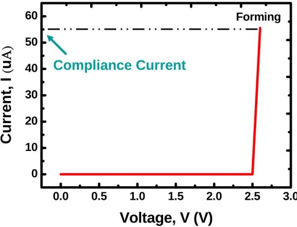
3.2.1 Compliance Current
The purpose for setting the compliance current is to prevent the RRAM from dielectric hard breakdown. There are two steps needed to be set for the compliance current. One is the step for “forming”; the other is the “set”. Generally speaking, the value of compliance current of “forming” is a few higher than that of “set”. This is because in the forming step, the conductive paths have to be formed. In this thesis, we set the compliance current through two different methods. In the 1R device, the compliance current is achieved by HP 4156C via the HT-BASIC language. And in the 1T1R device, the compliance current is achieved by the transistor through different gate voltage. In 1R device, the effect of limiting the current flow through the resistive random access memory is not ideal; because the
In contrast, the 1T1R structure is more reliable for conventional use as a result of excellent ability to limit the current flow through the resistive random access memory precisely.
3.2.2 The Predominant Step Before Resistive Switching - Forming
Before we start to operate the resistive switching random access memory correctly, we need to execute the so-called “forming” procedure first, as shown in Fig. 3.1. We add a ramped voltage on the top TiN electrode which is near the Ti buffer layer, and measure the corresponding current by HP 4156C semiconductor parameter analyzer. When the voltage is larger than the value which was
determined by the thickness of HfO2, the current rushs to the value of compliance current, and the
forming step is accomplished, as shown in Fig. 3.2.
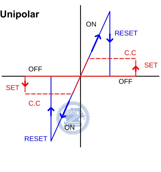
3.2.3 The Resistive Switching Characteristics - Uni-Polar and Bi-Polar
After the “forming” process, this device switches to LRS(Low Resistance State). The following step is to turn off it, which means to switch the RRAM from LRS to HRS(High Resistance State). There are two terminologies to identify the switching type of RRAM [3.1]. As shown in Fig. 3.3 and Fig. 3.4, one is uni-polar, and the other one is bi-polar. Uni-polar means that the turn on voltage and turn off voltage are in the same polarity, where the turn on voltage is usually larger than turn off voltage. The cell remains “ON” state until the sweep voltage exceeds the turn off voltage. The cell remains “OFF” state until the sweep voltage exceeds the turn on voltage. The uni-polar switching characteristic had been observed from many different switching materials. For example, D. Choi et al.[3.2] presented
the uni-polar characteristic for the SrTiOx thin film. C. Rohde et al. [3.3] demonstrated the uni-polar
characteristic for the TiO2 thin film. On the other hand, the bi-polar means that the turn on voltage and
turn off voltage are in opposite polarities. The bi-polar switching characteristic had been observed from many different switching materials, too. For example, K. Szot, W. Speier, et al. [3.4] demonstrated the
bi-polar characteristic for the SrTiO3 thin film. L. E. Yu et al. [3.5] presented the bi-polar characteristic
for the TiOx thin film. The illustrations of sweep operation in this thesis are shown in Fig. 3.5.and Fig.
3.6 and obviously our device is switched through bi-polar type.
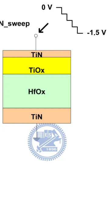
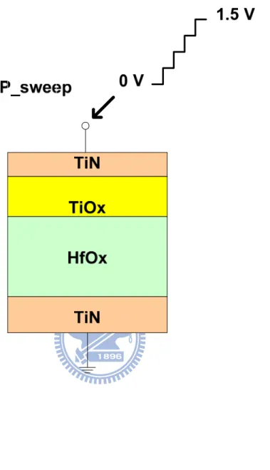
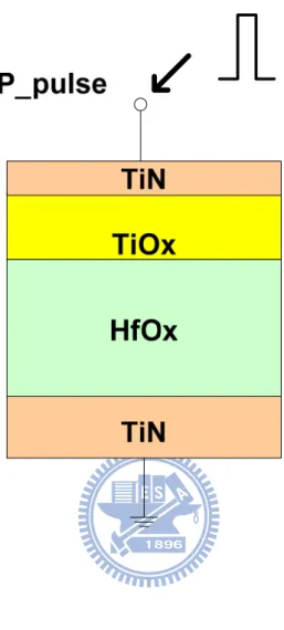
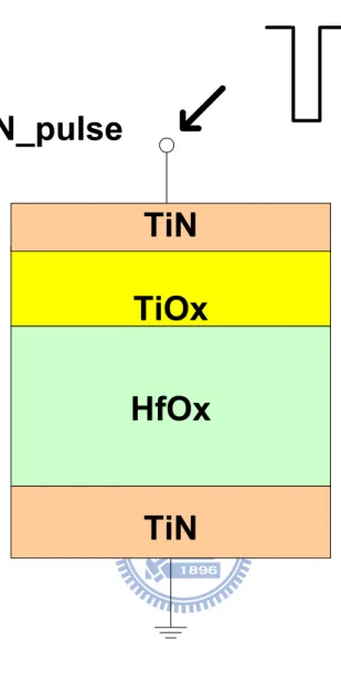
3.2.4 The Pulse Operation of RRAM
Besides the sweep operation, there is still another operate method for RRAM- pulse operation, and this kind of operation method is more practical for conventional use, as shown in Fig. 3.7 and Fig. 3.8. The pulse width we used in this thesis is about 10 ns.
3.2.5 The Switching Parameter Definitions of RRAM
The main parameters used in our thesis are shown in Fig. 3.9. When the device is switched to LRS,
we define Vset as the turn on voltage, and Iset as the corresponding current. When the device is switched
to HRS, we define Vreset as the turn off voltage and Ireset as the corresponding current. We also define the
maximum negative sweep voltage as Vstop.
There is still one question which has not been mentioned yet. How do we define the resistance of this device? In general, we read the current at 0.1V, and use the Ohm Law V = IR to obtain the resistance of this device. The “Forward Read” and “Reverse Read” technique are applied to RRAM, as we used popularly for the conventional memory device. Reading at voltage 0.1V stands for “Forward Read”, while reading at -0.1V means “Reverse Read”.
3.3 Reliability Issue
3.3.1 Effect of Electrode Area on Resistive Switching Properties
As shown in Fig. 3.10, the “Forming” voltage is dependent on the thickness of HfO2. Vforming is
about 2.5V for HfO2 thickness 5 nm while Vforming is about 3V if the thickness is 10 nm. Once the
thickness is down to 3 nm, the “Forming” procedure is ignored. Fig. 3.11 indicates that the Vforming, Vset
and Vreset are all independent of the cell size. This characteristic of independency of the cell area is one
of the advantages of RRAM.
3.3.2 Multi-Level Operation of RRAM
The multi-level operation is one of the other advantages of RRAM. Fig. 3.12 and Fig. 3.13 show
the possibility of multi-level operation. If we change the Vstop, the corresponding Vset will be different.
If we change the Iset, the corresponding Ireset will be different too. Obviously, the corresponding
resistance will be different .Multi-level operation will be helpful for cell size scaling, and this characteristic will help us design a cell with more selectivity.
3.3.3 Data Retention Characteristics of RRAM
The other important reliability issue of memory cells is its data retention ability. We can achieve the multi-level states by two operation methods. One is the sweep mode, just as we mentioned in section 3.3.2, and the other one is the pulse operation. For data retention characteristic, we achieved the different resistance levels by pulse operation, and the data writing for six level resistance states has been demonstrated by varying the amplitude of 10 ns voltage pulse. In Fig. 3.14, the multi-level is
we can obtain six different levels on one cell, and it is still maintains distinct levels after 1,000 seconds.
3.3.4 Program/Erase Cycling Endurance
In this section, we compare the cycling endurance of 1R and 1T1R device structures, where the HP 4156C and transistor are used for the current limiter respectively. As shown in Fig. 3.15 and Fig. 3.16, we can see the program/erase cycling endurance for the 1T1R and 1R devices respectively. The operational condition of 1R device structure is positive pulse 2.5V, negative pulse -3.6V, and the pulse width being 20ns for positive pulse and 80 ns for negative pulse respectively. For 1T1R device structure, positive pulse is 2.V, negative pulse is -3V and the pulse width are both 10 ns for positive and
negative pulse. The RRAM still behaves well and the window reaches three orders after at least 104
cycle times. We also observe program/erase cycling endurance degradation for the 1R device.
It could be the dielectric breakdown induced by the overshooting current which is not limited well with Agilent 4156C. From this experiment, we can understand the importance of the transistor in RRAM. With different gate voltages, we can control the compliance current precisely through the transistor, which was fabricated with advanced 0.18 um CMOS technology.
3.3.5 Read Disturb Immunity and temperature effect on RRAM
Fig. 3.17 shows the read disturb immunity of the stored bit by constant voltage stress at 1V. As we can see, the resistance is still a constant after stress voltage 1V with 1,000 seconds. In this experiment, we did not set any compliance current.
can see, at higher temperature, the maximum stress voltage is degraded to 0.7V. In Fig. 3.19, we show
the temperature effect for sweep mode. The parameters Vset、Vreset are almost the same. From these data,
TiOx
HfOx
TiN
Forming
TiN
Fig. 3.1 The cross section of transition metal oxide based resistive switching
0.0
0.5
1.0
1.5
2.0
2.5
3.0
0
10
20
30
40
50
60
Current, I
(
u
Α
)
Voltage, V (V)
Forming
Compliance Current
ON
OFF
ON
OFF
C.C
C.C
SET
RESET
RESET
SET
Fig. 3.3 Unipolar switching- Sketch of the resistive switching characteristics in a
voltage sweep experiment. C.C denotes the current compliance. The set voltage is always higher than the voltage at which reset takes place, and
RESET
SET
C.C
Fig. 3.4 Bipolar switching- Sketch of the resistive switching characteristics in a voltage
sweep experiment. C.C denotes the current compliamce. The set operation takes place on one polarity of the voltage or current, the reset operation requires the opposite polarity.
Fig. 3.5 Scheme of the negative sweep (Reset) operation in transition metal oxide
Fig. 3.6 Scheme of the positive sweep (Set) operation in transition metal oxide
Fig. 3.7 Scheme of the positive pulse (Erase) operation in transition metal oxide
Fig. 3.8 Scheme of the negative pulse (Program) operation in transition metal oxide
-1.5
-1.0
-0.5
0.0
0.5
1.0
1.5
0.01
0.1
1
10
100
1000
Cur
rent, I
(
u
Α
)
Voltage, V (V)
V
setI
setV
resetI
reset,maxV
stopC.C
Fig. 3.9 Typical current-voltage characteristics of TiN/Ti/HfO2/TiN thin film based resistive
switching memory. C.C denotes the current compliance. Vstop denotes the maximum
negative sweep voltage. Vreset or Ireset,max are the voltage or current at which reset
0
2
4
6
8
10
12
0
2
4
6
8
Forming V
o
ltage, V
forming(V
)
HfO
2thickness (nm)
Fig. 3.10 HfO2 thickness dependence of the forming voltage on TiN/TiOx/HfOx/TiN thin film based
0.1
0.2
0.3
0.4
0
2
4
6
Forming v
olta
ge, V
fo rm in g(V)
Cell Size
(
um
2)
(a)0.1
0.2
0.3
0.4
-2
-1
0
1
2
Vo
lt
ag
e,
V (V)
Cell Size
(
um
2)
V
SETV
RESET(b)
Fig. 3.11 Cell sizes dependence of various resistance switching parameters in 1R
configuration. (a) Forming voltage (Vforming), (b) Set voltage (Vset) and
-1.5
-1.0
-0.5
0.0
0.5
1.0
1.5
10
-510
-410
-3Current, I (A)
Voltage, V (V)
D
-1.5
C
-1.1
B
-0.8
A
-0.6
A
B
C
D
-1.5
-1.0
-0.5
0.0
0.5
1.0
1.5
10
-610
-510
-410
-3Current, I (A
)
Voltage, V (V)
A
0.1mA
B
0.5mA
C
1mA
D
3mA
A
B
C
D
A
B
C
D
100
1k
10k 100k 1M 10M 100M
10k
100k
1M
10M
100M
Level 6
Level 5
Level 4
Level 3
Level 2
Resistance, R
(
Ω
)
Time, t (sec)
Level 1
10 yr
Fig. 3.14 Data Retention properties of various states in multi level operation. The result
0
2000 4000 6000 8000 10000
1E-3
0.01
0.1
1
10
Resistance, R
(ΜΩ
)P/E Cycle Number (Time)
1T1R
P_pulse = 2V
N_pulse = -3V
Pulse Width= 10 ns
Fig. 3.15 Superior pulse dependent switching property in 1T1R configuration by 10ns
0
2000 4000 6000 8000 10000
1E-3
0.01
0.1
1
Resi
stance,
R
(ΜΩ
)P/E Cycle Number (Time)
1R
P_pulse = 2.5V, 20 ns
N_pulse = -3.6V, 80 ns
Fig. 3.16 Switching property in 1T1R configuration by 10ns pulse. There is a little
window degradation after 104 cycles. The set pulse height is 2.5V, while
reset pulse height is -3.6V, respectively. And the pulse width is longer than the pulse width in 1T1R configuration.
0
200
400
600
800
1000
0.0
0.5
1.0
1.5
2.0
2.5
3.0
3.5
4.0
Resistance, R
(
ΜΩ
)
Stress Time, t (second)
Vstress = 1 V
Fig. 3.17 Read disturb immunity of RHigh by constant voltage stress of 1 V for
0
200
400
600
800
1000
0.5
1.0
1.5
2.0
2.5
3.0
3.5
4.0
Resistan
ce, R
(ΜΩ
)Stress Time, t (second)
V
stress
=0.7V
T=85oC
Fig. 3.18 Read disturb immunity of RHigh by constant voltage stress of 0.7V at 85 for ℃
-1.5
-1.0
-0.5
0.0
0.1
1
10
100
Current
, I
(
μΑ)
Voltage, V (V)
300 K 330 K 360 K 400 K (a)-0.2 0.0 0.2 0.4 0.6 0.8 1.0 1.2 1.4 1.6
50
100
150
200
Cu
rrent,
I
( μΑ )Voltage, V (V)
300 K
330 K
360 K
400 K
(b)Fig. 3.19 Typical I-V characteristic of the transition metal oxide thin film based
resistive switching memory under different temperature. (a) Reset (b) Set.
Chapter 4
Switching Mechanism of 1R and 1T1R Resistive Memory
4.1 Introduction
In this chapter, we investigate the basic switching properties of RRAM from the point of the “forming” process, which is like the phenomenon of the dielectric soft breakdown. With the known mechanism of SBD on High-κ MOSC (MOS Capacitor), we will compare the difference between RRAM and MOSCs on resistive switching. It could be realized that the unique “forming” process of RRAM’s comes from its different electrodes between MOSC’s. Furthermore, with its resistance switching phenomenon, we could be able to explain and extinguish the “Multi–read” operation in RRAM. Besides, having the established RTN measurement procedure, the possible mechanism of its resistance switching could be more clear.
4.2 The Predominant Step Before Resistive Switching - Forming
4.2.1 The Resistive Switching Characteristics after Dielectric Soft Breakdown
Even the “forming” phenomenon is said like “Soft Breakdown”(SBD)which we are familiar under MOS device [4.1], there would be more complete explanation for its phenomenon on RRAM’s resistive switching. Fig. 4.1 is the definition of soft breakdown [4.2].
With the opaque relation between “forming” and SBD, we take exercise on a High–κ MOSC about its SBD. The physical thickness of its dielectric is 2 nm, and the stress condition is 2.4 V, 400
seconds. The SBD phenomenon is observed in Fig. 4.2. The resistance comes to 1012 Ω, which is more
resistance still reaches 109 Ω (Fig. 4.3). The forming voltage is about 9.2 V which is larger than the RRAM we used in this thesis. From this exercise, the MOSC is still in HRS (Fig. 4.4) instead of switching to LRS under the hypothesis on the connection between SBD and “forming”.
The difference may come from the different top electrodes of RRAM and MOSC. It is TiN with a Ti buffer layer for RRAM and poly-silicon for MOSC. Ti is well known for its ability to absorb the
oxygen atoms from HfO2 [4.3] when growing TiOx/HfOx thin film which has advanced performance
than ZrO2 thin film [4.4] for resistive switching RRAM applications [4.5]. The abundant oxygen
vacancies in TiOx leads to excellent resistive switching characteristic.
If the conductive path (filament) is formed in oxygen deficient TiOx and HfOx layers, as the
thickness of HfO2 drops to 3nm, the predominant soft breakdown procedure (forming) is not necessary
[4.6]. The negative charged oxygen ions move toward the anode side (TiN with Ti buffer layer), and
the oxygen deficient conductive path goes deep into the HfO2 layer which is thicker than 5nm when
operation forming action on the RRAM. The phenomenon is more like SBD in the high-κ dielectric. It could be imagined that the oxygen deficient path is formed by the so called oxygen vacancy, and the movement of the oxygen vacancies toward the anode side or cathode side leads to resistive switching.
Otherwise, SBD is exercised on RRAM with stress time 500 seconds (Fig. 4.5). However, the
resistance is unchanged (~1012Ω). The stress continuous and strengthen until the lower resistance for
“forming “operation is accomplished (Fig. 4.6). After that, the resistance lowers to about 0.6KΩ liking the LRS of forming. Moreover, this device stays in LRS without resistive switching even the operation bias is off (Fig. 4.7). We could realize that the device is over forming.
more than the latter.
4.2.2 The Effect of Resistive Switching Properties by Reverse Operation
If we reverse the electrode (the TiN electrode without Ti buffer layer is connect to the apply voltage and the TiN electrode with Ti buffer layer is ground) , as we can see in Fig. 4.8, the forming voltage is larger than 3V. But the thickness of this device is only 5 nm, and the reasonable forming voltage is 2.5 V.
After the “forming” procedure on RRAM, the ideal bi-polar switching characteristic is expected. However, it is not easy to be realized. The oxygen vacancy plays an important role of the “forming” operation. Since the oxygen vacancies were repelled deeper near the bottom electrode when we operating “forming” under the normal direction, the resistive switching could be enhanced from their migration. On the other hand, when we operate “forming” under the reverse direction, the oxygen
vacancies were repelled to the top electrode far away from the HfO2 bulk layer. The resistive switching
is opaque with oxygen vacancies absence for carrier transportation main path.
4.3 Resistance Switching
4.3.1 Multi - Read Operation
The “Multi-Read” operation for this device is observed and other interesting phenomena are discussed in this section. As we mentioned in Ch. 3, we define the HRS and LRS with the Ohm Law V= IR by read the current at 0.1V and -0.1V. If the resistance is from low (high)to high(low), the operation is defined program(erase). Now, if RRAM is programmed to HRS, then we read it under different voltages, the “Multi-Read” (Fig. 4.9). As we can see, the read current increases with
corresponding voltage without resistance differing.
To make sure that we did not change the state or destroy the device by read it with a larger voltage, we recheck the resistance at 0.1V and -0.1V and read disturb immunity by constant voltage stress of 1V for 1,000 seconds (Fig. 4.10). It is reconfirmed at the static state after the “multi-read” operation.
This is interesting because we can get different resistance through different read voltage without change its resistance state or destroy the device. No matter what initial resistance state it is, the “non-linear” phenomena can still be found with the “multi-read” operation, as shown in Fig. 4.11, Fig. 4.12, Fig. 4.13 and Fig. 4.14, respectively. But the maximum read voltage is decreasing as the initial resistance is getting lower and lower.
4.3.2 Measurement of Random Telegraph Noise on RRAM
From the structure of this device, the trapping and de-trapping of carrier charge in defect states
near the TiOx/HfOx dielectric interface and related modulation in carrier mobility and density may be
the reason of resistive switching. The RTN measurement is shown in Fig. 4.15. The fluctuation amplitude is related to the voltage as shown in Fig. 4.16. The most interesting phenomenon is that the RTN can only be observed under HRS(Mega Ohm)state. We can not have any RTN in LRS and un-forming state.
I. G. Baek et al. [4.7] demonstrated that the metal or oxygen vacancies could create density of
states near the valance or conduction band respectively while the metallic defects create density of states just above the Fermi level of the electrode as shown in Fig. 4.17 and Fig. 4.18.
above Fermi level when RRAM is in low resistance state. There is any density of state exist within the downward bending band when adding positive bias to anode. This is the reason for absence of RTN signal when RRAM in low resistance state. On the contrary, there are lots of densities of states within the downward bending band when RRAM in high resistance state having distinct empty metallic states below the Fermi level. This is the reason of RTN signal when RRAM in high resistance state.
4.3.3 Summary
The “forming” is to produce a channel through the switching layer by oxygen vacancy movement and companion with the SBD in the dielectric. We believe that the conducting path which consists of
oxygen deficient TiOx is nucleated through the resistance switching layer, and it explains when the
thickness of HfO2 is decreased to 3nm, the predominant soft breakdown procedure (forming) is not
necessary.
When the percolation of oxygen vacancies goes deeply into the HfO2 layer, it goes to a low resistance state of RRAM, and then the metallic density of states are empty, companion with the increasing current. This phenomenon could be confirmed with SCLC theory by fitting the I-V data measured at the low resistance state. On the other hand, when we add a negative polarity voltage on the
top electrode, the oxygen vacancies leave from the deep of HfOx, then the metallic density of states are
filled with these oxygen states, followed by the decreasing current, and the channel between the bottom electrode and the switching layer become incomplete. Therefore, the resistance state of RRAM goes to high resistance state.
The multi-levels which were achieved by pulse operation may be the result of the many intermediate resistance states caused by the tiny multi filament between the resistive switching layer. Depending on the movement of oxygen vacancies, the conductive path is either formed or disappeared.
This is the suggested resistive switching mechanism for the binary metal oxide based resistive random access memory.
In high resistance state, lots of oxygen vacancies concentrate between the interface of Ti buffer layer and HfO2 switching layer. It is well known that defects of transition metal oxide thin films generate impurity states in the band gap. Therefore, ample trap sites within the interface result to RTN in high instead of low resistance state.
When reversing the operation mode, oxygen vacancy instead of digging into HfO2 switching layer
would move into TiOx high-k layer. It results to conductive path from soft breakdown. It could explain
the larger forming voltage and a worse resistance switching performance when reversing the operation mode.
0
100
200
300
400
500
10
-310
-210
-1Current
, I
(
μΑ
)
Stress time, t (second)
Physical thickness = 2 nm
V
stress= 2.4 V
High-K MOSC
Fig. 4.2 Current-Voltage characteristic under constant voltage source stress of the high- κMOSC. The physical thickness of the dielectric layer is 2 nm. And, we can
0
2
4
6
8
10
-20.0
0.0
20.0
40.0
60.0
80.0
100.0
120.0
140.0
Cur
rent,
I
(
μΑ
)
Voltage, V (V)
MOSC
Forming
Fig. 4.3 The current-voltage characteristic of high-κ MOSC after the predominant step-forming. The forming voltage is about 9.2V.
0.0
0.5
1.0
1.5
2.0
0.0
0.1
0.2
0.3
0.4
Current
, I
(
nA
)
Voltage, V (V)
MOSC
Fig. 4.4 The current-voltage curve of high-κ MOSC under resistive switching test. There is no hysteresis phenomenon when we sweep the voltage from 0V to 2V, and then back to 0V.
0
100
200
300
400
500
0
5
10
Cur
rent,
I
(pA
)Stress tim e, t (second)
V
stress= 2.4 V
RRAM
(a)0
100
200
300
400
500
0.1
1
10
Cu
rren
t, I
(pA
)Stress time,t (second)
V
stress= 2.4 V
RRAM
(b)
Fig. 4.5 After constant voltage stress 2.4V for 500 seconds, the soft breakdown phenomenon of resistive switching memory device is observed. The
0
500
1000
1500
0
1
2
3
4
5
6
Cu
rren
t, I
(mA
)Stress time, t (second)
RRAM
V
stress= 2.4 V
(a)0
500
1000
1500
10
-1310
-1110
-910
-710
-510
-310
-1Current
, I
(A
)Stress time, t (second)
RRAM
V
stress= 2.4 V
(b)
Fig. 4.6 Current-Voltage characteristic of RRAM by constant voltage stress 2.4V for 1500 seconds. The physical thickness of the dielectric layer is 5 nm. And the forming-like phenomenon is found.
-1.5
-1.0
-0.5
0.0
0.0
0.5
1.0
1.5
2.0
2.5
3.0
Current, I
(mA
)Voltage, V (V)
Fig. 4.7 The current-voltage curve of RRAM under resistive switching test. There is no hysteresis phenomenon when we sweep the voltage from 0V to -1.6V, and then back to 0V.
-0.5 0.0 0.5 1.0 1.5 2.0 2.5 3.0 3.5
-20
0
20
40
60
80
100
120
140
160
C
u
rrent, I
(μΑ
)Voltage, V (V)
Fig. 4.8 The effect of resistive switching characteristic by reverse operation. The forming is about 3.2V, when we exchange the electrodes.
-1.5 -1.0 -0.5
0.0
0.5
1.0
1.5
-20
0
20
40
60
80
100
120
140
160
Resist
ance, R
(ΜΩ
)Read Voltage, V (V)
Forward read Reverse readNon-linear
Rrsistance
(a)0.0
0.5
1.0
1.5
0.0
0.5
1.0
1.5
2.0
Current, I
(mA
)Read Voltage, V (V)
(b)0
200
400
600
800
1000
0.0
0.5
1.0
1.5
2.0
2.5
3.0
3.5
4.0
Resist
an
ce, R
(ΜΩ
)Stress Time, t (second)
Vstress = 1 V
-1.5 -1.0 -0.5
0.0
0.5
1.0
1.5
0
200
400
600
800
Resist
an
ce, R
( ΚΩ )Read Voltage, V (V)
(a)0.0 0.2 0.4 0.6 0.8 1.0 1.2 1.4 1.6
0.0
0.5
1.0
1.5
2.0
2.5
Current, I
(mA
)Read Voltage, V (V)
(b)Fig. 4.11 The multi read characteristics when the resistance is 800KΩ at +0.1V and -0.1V. (a) resistance- voltage curve. (b) current-voltage curve
-1.0
-0.5
0.0
0.5
1.0
0
100
200
300
400
500
Resist
ance, R
(ΚΩ
)Read Voltage, V (V)
(a)0.0
0.2
0.4
0.6
0.8
1.0
1.2
0.0
0.5
1.0
1.5
Curr
ent. I
(mA
)Read Voltage, V (V)
(b)Fig. 4.12 The multi read characteristics when the resistance is 500KΩ at +0.1V and -0.1V. (a) resistance- voltage curve. (b) current-voltage curve
-1.0
-0.5
0.0
0.5
1.0
0
50
100
150
200
250
300
Resi
st
an
ce,
R
(ΚΩ
)Read Voltage, V (V)
(a)0.0
0.2
0.4
0.6
0.8
1.0
1.2
0.0
0.5
1.0
1.5
Curren
t,
I
(mA
)Read Voltage, V (V)
(b)Fig. 4.13 The multi read characteristics when the resistance is 300KΩ at +0.1V and -0.1V. (a) resistance- voltage curve. (b) current-voltage curve
-1.0
-0.5
0.0
0.5
1.0
0
1
2
3
4
5
6
Resistance, R
(ΚΩ
)Read Voltage, V (V)
(a)0.0
0.2
0.4
0.6
0.8
1.0
1.2
0.0
0.5
1.0
1.5
Cu
rren
t, I
(mA
)Read Voltage, V (V)
(b)Fig. 4.14 The multi read characteristics when the resistance is 6KΩ at +0.1V and -0.1V. (a) resistance- voltage curve. (b) current-voltage curve
1
2
3
4
5
6
7
0.3
0.4
0.5
0.6
0.7
0.8
0.9
1.0
1.1
1.2
Current, I
(
μΑ
)
Time, t (second)
0.5V
0.55V
0.6V
0.65V
0.7V
0.75V
0.8V
0.9V, 1V, 1.1V
Fig. 4.15 RTN current waveform of high resistance state transition metal oxide thin film based resistive switching memory. The fluctuation amplitude increases slightly as the voltage increase from 0.5V to 0.8V. If the voltage is high than 0.8V or lower than 0.5V, there is no RTN signal.
0.50 0.55 0.60 0.65 0.70 0.75 0.80
0.01
0.014
0.015
0.024
0.0243
0.025
0.027
Percentage (
%)
Voltage, V (V)
Fig. 4.16 The percentage of RTN signal fluctuation amplitude. As the voltage increase from 0.5V to 0.8V, the fluctuation amplitude increase too.
Fig. 4.17 The band diagram of an electrode and transition metal oxide in LRS. The metallic state is located above the Fermi level.
Fig. 4.18 The band diagram of an electrode and transition metal oxide in HRS. The metallic state is located below the Fermi level.