國
立
交
通
大
學
電子工程學系 電子研究所
碩 士 論 文
以準分子雷射退火製作控制晶界位置之多閘極
複晶矽薄膜電晶體之研究
Study on the Polycrystalline Silicon Thin Film Transistors with
Location-Controlled Grain Boundary and Multi-Gate Structure
Using Excimer Laser Annealing
研 究 生:李序恒
Syu-Heng Lee
指導教授:鄭晃忠 博士
Dr. Huang-Chung Cheng
以準分子雷射退火製作控制晶界位置之多閘極
複晶矽薄膜電晶體之研究
Study on the Polycrystalline Silicon Thin-Film Transistors with
Location-Controlled Grain Boundary and Multi-Gate Structure
Using Excimer Laser Annealing
研 究 生:李序恒 Student : Syu-Heng Lee
指導教授:鄭晃忠 博士 Advisor : Dr. Huang-Chung Cheng
國立交通大學
電子工程學系 電子研究所碩士班
碩士論文
A Thesis
Submitted to Department of Electronics Engineering
& Institute of Electronics
College of Electrical and Computer Engineering
National Chiao-Tung University
In Partial Fulfillment of the Requirements
For the Degree of Master
In
Electronics Engineering
July, 2008
Hsinchu, Taiwan, Republic of China
以準分子雷射退火製作控制晶界位置之多閘極複晶矽
薄膜電晶體之研究
研究生:李序恒 指導教授:鄭晃忠 博士
國立交通大學
電子工程學系 電子研究所碩士班
摘要
近年來,低溫複晶矽薄膜電晶體成為顯示技術應用中的關鍵元件,由於其高 載子遷移率的特性可以應用在系統面板(System on Panel, SOP)上。雖然透過 傳統準分子電射退火方式可轉化非晶矽薄膜成為複晶矽,但此方法仍有些許缺 點,如較狹窄的雷射製程條件、小晶粒與隨機分佈的晶粒邊界隨機分佈等等。在 這篇論文裡,我們提出一種易於控制雷射結晶方式,並利用該雷射結晶方式配合 多閘極結構來增進複晶矽薄膜電晶體的特性。在 第 一 部 份 , 我 們 提 出 一 種 稱 為 氧 化 矽 臺 階 式 通 道 結 晶 法 (Recessed-Channel with Oxide Step Method)之側向結晶方式,應用於製作
可控制晶粒邊界位置之低溫複晶矽薄膜電晶體並加以探討,我們分析此種控制晶 粒邊界位置技術之結晶機制分為山脊區與凹陷區之結晶:當雷射照射在凹陷區並 使得完全熔融時,氧化矽側壁有較厚之未熔融矽薄膜作為晶種,晶粒便會在凹陷 區作側向成長;當雷射照射在長度為 2μm之山脊區時,由於山脊區中間部份比 邊緣儲熱時間較久,故先有矽晶種產生且成長為小晶粒,阻擋由氧化矽側壁向山 脊區中央側向成長之晶粒,我們把山脊區長度縮減為 1.5 μm則可避免此現象; 我們可以到均勻且方向一致的大型多晶矽晶粒分佈之複晶矽薄膜,因此可提升薄 膜的均勻性與元件的效能。此外,我們利用掃描式電子顯微鏡、掃瞄原子力顯微 鏡對控制晶粒邊界之複晶矽薄膜層分析,我們觀察到在谷區中有約 1.5 μm長的 人為控制晶粒,在山脊區有約 0.75 μm長的人為控制晶粒。我們也利用此結晶 方式製作出單一主要晶粒邊界的低溫複晶矽薄膜電晶體,並對其電特性加以研 究。在無氫化過程處理下,其P型元件之場效載子移動率可達到 168 cm2 /V-s, 其次臨界擺幅與汲極誘導體能障下降可達 0.226 V/decade和 310 mV。同時我們 也比較製作元件於谷區與山脊區的各項電特性,在固定山脊區長度為 2μm條件 下,山脊區中間因有小型晶粒分佈,使得元件製作於山脊區之電特性較製作於谷 區差,其製作於山脊區之元件的場效載子移動率為 99 cm2 /V-s。 儘管單一主要晶粒邊界之複晶矽薄膜電晶體表現出良好的電特性,然而在元 件通道中的單一主要晶粒邊界仍會對電特性產生影響。因此在第二部份,我們引 入多閘極結構,研究避開單一晶粒邊界影響之電特性。在沒經過任何氫化處理過 程下,P型元件之場效載子移動率更超過 190 cm2 /V-s。量測二十個元件的均勻 性,場效載子移動率標準差小於 30 cm2 /V-s,臨界電壓的標準差小於 0.78 V, 次臨界擺幅之標準差 0.113 V/decade。透過多閘極之結構,我們可以觀察到陡 峭之次臨界擺幅,其可達 0.164 V/decade。另外相較於傳統結晶方式之多閘極 複晶矽薄膜電晶體,我們也獲得 6 倍以上之驅動電流。
Study on the Polycrystalline Silicon Thin Film Transistors
with Location-controlled Grain Boundary and Multi-Gate
Structure Using Excimer Laser Annealing
Student: Syu-Heng Lee Advisor: Dr. Huang-Chung Cheng
Department of Electronics Engineering & Institute of Electronics
National Chiao Tung University
ABSTRACT
In recent years, polycrystalline silicon (poly-Si) thin film transistors (TFTs) were the key devices in flat-panel display technology and System on a Panel (SOP) applications due to its high mobility. Although conventional excimer laser can transfer amorphous Si to polycrystalline Si in order to fabricate poly-Si TFTs. There were still some disadvantages such as narrow laser process window, random small grain and grain boundaries, and etc.. In this thesis, therefore, we proposed a method, which is so called Recessed-Channel with Oxide Step method, to control the grain growth and grain boundary. With the benefits of this crystallization method and multi-gate structure, high performance multi-gate poly-Si TFTs had been fabricated with no main grain boundary in the channel region.
At the first part, single grain boundary (SGB) thin film transistors (TFTs) fabricated by excimer laser annealing were investigated. The crystallization mechanisms of valley region and ridge region of Recess-Channel with Oxide Step method were studied. A thick amorphous silicon region was formed in the sidewall of
oxide step which acted as the seeds for the grain lateral growth during excimer laser irradiation. As the excimer energy density was controlled to completely melt the amorphous silicon thin film of valley region and partially melt the thick part in the sidewall of the oxide step. The lateral growth grain would be observed in the valley region. When laser irradiated the ridge region with channel length of 2 μm, the holding time of thermal energy of the edge of the ridge region was longer than that of the center of the ridge region. There were small grains in the middle of the ridge region, and the small grains obstructed the growth of the lateral grains from the sidewall to the center. We decreased the length of the ridge region to 1.5 μm, the phenomenon of grain obstruction would be eliminated. Therefore, the lateral growth grain starting from un-melt silicon seeds could extend along the opposite direction toward the complete melt valley region and ridge region. Thus, a uniform and large grain of polycrystalline silicon film would lead to improved device performance. According to the analysis of scanning electron microscope (SEM) and atomic force microscope (AFM), large longitudinal grains were observed to be about 1.5 μm in valley region and about 0.75 μm in ridge region. The electrical characteristics of single grain boundary TFTs fabricated by Recessed-Channel with Oxide Step TFTs were also investigated. High performance p-type SGB-TFTs with field-effect mobility reaching 168 cm2/V-s had been fabricated without any hydrogenation treatment. The subtheshold swing and drain-induced-barrier-lowing (DIBL) of SGB-TFTs were 0.226 V/decade and 310 mV respectively. In addition, the electrical characteristics of devices located on the valley region and ridge region were studied. While the length of ridge region was 2μm, there was a small grain region in the middle of ridge region. Because the crystalline of ridge region of poly-Si thin film was defective, the electrical characteristics of devices located on ridge region were poorer than that of
region was 99 cm2/V-s.
Although SGB-TFTs exhibited high performance, the electrical characteristics of SGB-TFTs were affected by the single main grain boundary located in device channel. Hence, we introduced the multi-gate (MG) structure to eliminate the single grain boundary effect and investigated the electrical characteristics of multi-gate TFTs in order to avoid the single main grain boundary in the channel. High performance p-type MG-TFTs with field-effect mobility exceeding 190 cm2/V-s had been fabricated without any hydrogenation treatment. The characteristics of twenty MG-TFTs devices were taken into discussion. The standard deviation of equivalent field-effect mobility was smaller than 30 cm2/V-s and the standard deviation of Vth was smaller than 0.78 V, while that of subthreshold swing was smaller than 0.113 V/decade. By means of multi-gate structure, the steeper subthreshold swing reaching 0.164V/decade was obtained. Furthermore, MG-TFTs provided 6 times higher driving current than conventional TFTs.
誌
謝
感謝我的碩士論文指導教授 鄭晃忠博士教導我在實驗、論文上的嚴謹態度 及謙恭溫和的待人處事,讓學生受益許多。 感謝蔡春乾學長與韋凱方學長帶我進入低溫多晶矽薄膜電晶體的領域,兩位 學長除了原諒我在作人處事上的無知與實驗上的懶惰之外,還在休息時間被我的 實驗上問題打擾及給我各方面問題的指點,同時分享生活上的趣事與不斷的幫我 打氣加油,真的很感謝你們在我碩士生涯中的幫助。 感謝李逸哲學長與楊柏宇學長在我碩士生涯後半年的指導,教導許多量測知 識,同時在量測累的時侯鼓勵我。 感謝 TFT 組的學長,同學,學弟妹,謝謝你們使得我的兩年碩士生涯增加許 多樂趣,其中包括張國瑞學長、廖大傳學長、王祐祈學長、劉全豐學長、林心瑜 學姐、涂仕煒同學、林偉凱同學、劉政欽同學、胡明哲學弟、鄧茜云學妹、徐邦 祐學弟、陳聖凱學弟。 感謝 CNT 組的學長,同學,學弟,謝謝你們使得我在實驗室的日子快樂不少, 其中包括林高照學長、張加聰學長、張佩琪學姐、陳俠威學長、柳耀星學長、林 君翰學長、許育瑛同學,李建穎同學、魏英彰學弟、蔡萬霖學弟。 感謝老師的助理們,感謝你們在行政上的協助幫忙,其中包括碧蓮助理、依 婷助理及采綸助理。 感謝國家奈米中心的裡常幫助我的工程師與技術員,由於你們在實驗機台上 的幫助,使得我能完成實驗,特別是彭馨誼小姐、鄭旭君先生、吳志明先生、薛 富國先生、趙子綾小姐、林婉貞小姐、陳秉賢學長、簡秀芳小姐。 感謝我的父母與家人和親戚,感謝父母養育我從小到大,且伴我渡過在生活 中的困難;感謝哥哥姐姐伴我從小到大的生活;感謝親戚讓我離鄉仍有家的感覺。 感謝鄭晨薇小姐,感謝妳貼心的舉動,準備好的水果與加油打氣的字語帶給 我的支持動力。 感謝大學同學鄭淑媖同學,心情低落時常一起喝飲料討論工作與實驗。 最後,感謝所以幫助過我的朋友,謝謝你們。Contents
Abstract (in Chinese)……….i
Abstract (in English)……….iii
Acknowledgements (in Chinese)...vi
Contents………...vii
Table Lists…...………. x
Figure Captions………..………..…xii
============================================================= Chapter 1 Introduction……….………...1
1.1 Overview of Low-Temperature Polycrystalline Silicon (LTPS) Thin-Film Transistors (TFTs)………....………1
1.2 Overview of Crystallization of Amorphous Silicon Thin Films………..2
1.2.1 Solid Phase Crystallization of Amorphous Silicon Thin Films………..3
1.2.2 Metal Induced Crystallization of Amorphous Silicon Thin Films………….4
1.2.3 Laser Irradiation Crystallization of Amorphous Silicon Thin Films………..4
1.3 Ion activation………....8
1.4 Motivation...10
1.4.1 Fabrication of Polycrystalline Silicon Thin Films with Location-Controlled Grain Boundary Technology………..11
1.4.2 Polycrystalline Silicon Thin Film Transistors with Multi-Gate Structure by Recessed-Channel with Oxide Step Process………...12
1.5 Thesis Organization………..………..13
Chapter 2 Fabrication of Location-Controlled Single-Grain-Boundary (SGB) Polycrystalline Silicon (Poly-Si) Thin-Film Transistors (TFTs) by
Recessed-Channel with Oxide Step Methods Using Excimer Laser
Annealing (ELA)………...15
2.1 Introduction………..15
2.1.1 Introduction to Recessed-Channel with Oxide Step Methods…………...15
2.2 Material Analyses of Single Grain Boundary Polycrystalline Silicon Thin Films Fabricated by Elevated Channel Methods………. 20
2.2.1 Process Flow of Material Analyses of Location-Control SGB Poly-Si Thin Films Fabricated by Recessed-Channel with Oxide Step Method …...20
2.2.2 Material Analysis of Location-Controlled SGB Poly-Si Thin Film Fabricated by Recessed-Channel with Oxide Step Method………...21
2.2.2.1 Scanning Electron Microscope (SEM) Analysis………21
2.2.2.2 Transmission Electron Microscope (TEM) Analysis…………...24
2.3 Fabrication and Electrical Characteristics Analyses of Location-Controlled Single Grain Boundary (SGB) Polycrystalline Silicon (Poly-Si) Thin-Film Transistors (TFT) Fabricated by Recessed-Channel with Oxide Step Method………...…….25
2.3.1 Process Flow of SGB-TFTs by Recessed-Channel with Oxide Step Method……...……26
2.3.2 Electrical Characteristics of SGB-DG-TFTs……....………...27
2.4 Summary………29
Chapter 3 Investigation of Main Grain Boundary effect effect of Single-Grain-Boundary (SGB) Thin Film Transistors by Recessed-Channel with Oxide Step method...………....……31
3.1 Introduction………31
3.2 The Grain Boundary issue... ………...………32
Transistors by Recessed-Channel with Oxide Step method………..……….33
3.3.2 Process flow of MG-TFTs by Recessed-Channel with Oxide Step method.34 3.3.3 Electrical Characteristics Analysis MG-TFTs by Recessed-Channel with Oxide Step Method……….……...35
3.3.3.1 Improvement Comparison of MG-TFTs and SG-TFTs with/without Location-Controlled Grain Boundary Structure……….……...35
3.2.3.2 Electrical Characteristics of MG-TFTs by Recessed-Channel with Oxide Step Method ………..…….38
3.2.3.3 Uniformity of MG-TFTs by Recessed-Channel with Oxide Step Method………...40 3.4 Summary………....41 Chapter 4 Conclusions………..…………43 Table……….45 Figure Caption………....49 References………...82
Table lists
Chapter 2
Table 2-1 Measured optimal electrical characteristics of P-type SGB-TFTs fabricated by Recessed-Channel with Oxide Step method and conventional TFTs. The excimer laser energy density was 560mJ/cm2 and number of laser shot was 20 (ie. 95% overlapping)………...45
Table 2-2 Measured optimal electrical characteristics of P-type SGB-TFTs fabricated by Recessed-Channel with Oxide Step method were located above the valley region and ridge region, respectively. The excimer laser energy density was 560mJ/cm2 and number of laser shot was 20 (ie. 95% overlapping)………45
Chapter 3
Table 3-1 Measured optimal electrical characteristics of P-type MG-TFTs and SG-TFTs fabricated by Recessed-Channel with Oxide Step method. The excimer laser energy density was 560mJ/cm2 and number of laser shot was 20 (ie. 95% overlapping)………...45
Table 3-2 Measured optimal electrical characteristics of P-type MG-TFTs and SG-TFTs fabricated without any location-controlled grain boundary technology. The excimer laser energy density was 560mJ/cm2 and number of laser shot was 20 (ie. 95% overlapping)………46
Table 3-3 The improvement of electrical characteristics of devices with/without location-controlled grain boundary………46
Table 3-4 The improvement of electrical characteristics of different gate structure devices with/without location-controlled grain boundary………..47
Table 3-5 Measured optimal electrical characteristics of P-type MG-TFTs fabricated by Recessed-Channel with Oxide Step method and conventional MG-TFTs. The excimer laser energy density was 560mJ/cm2 and number of laser shot was 20 (ie. 95% overlapping)……….47
Table 3-6 Electrical characteristics of twenty measured P-type MG-TFTs fabricated by Recessed-Channel with Oxide Step method and conventional MG-TFTs. The excimer laser energy density was 560mJ/cm2 and number of laser shot was 20 (ie. 95% overlapping)……….48
Figure Captures
Chapter 2
Fig. 2.1 (a) The schematic illustration of the low energy regime corresponding to energy densities that partially melting the a-Si thin film………..49
Fig. 2.1 (b) The schematic illustration of the high energy regime corresponding to energy densities that completely melting the a-Si thin film………..49
Fig. 2.1 (c) The schematic illustration of the super lateral growth regime corresponding to energy densities that nearly completely melting the a-Si thin film……….49
Fig. 2.2 The schematic illustration of the grain growth regime of the Recessed-Channel structure by excimer laser annealing……….50
Fig. 2.3 The device diagram with Recessed-Channel method……….50
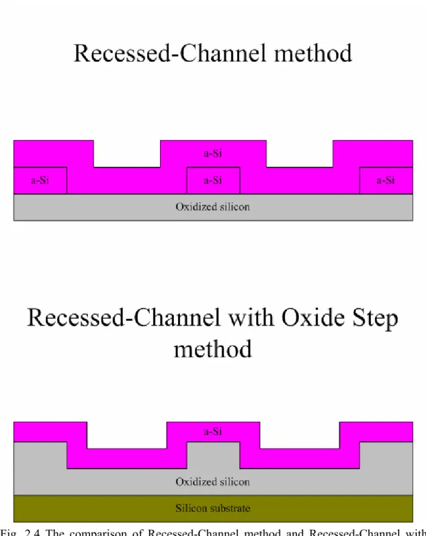
Fig. 2.4 The comparison of Recessed-Channel method and Recessed-Channel with Oxide Step method………51
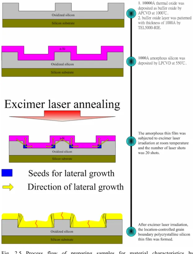
Fig. 2.5 Process flow of preparing samples for material characteristics by Recessed-Channel with Oxide Step method………52
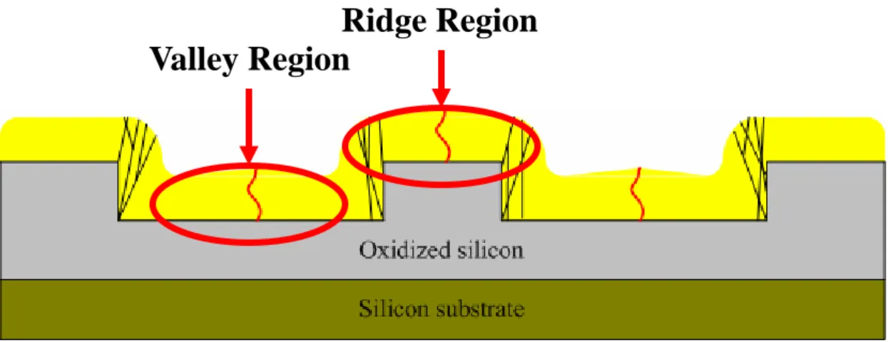
Fig. 2.6 The definition of valley region and the ridge region of the Recessed-Channel with Oxide Step structure……….53
was varied from (a) 1.5μm to (b) 3μm. The excimer laser energy density was
540 mJ/cm2………...53
Fig. 2.8 SEM graphs of exceimer laser crystallized polycrystalline silicon by Recessed-Channel with Oxide Step method. The length of the oxide ridge region was varied from (a) 1.5 μm to (b) 2 μm. The excimer laser energy
density was 480 mJ/cm2………54
Fig. 2.9 SEM graphs of the ridge region of exceimer laser crystallized polycrystalline silicon by Recessed-Channel with Oxide Step method. The length of the oxide ridge was 2 μm. The excimer laser energy density was varied (a) 600 mJ/cm2 (b) 540 mJ/cm2 (c)480 mJ/cm2……….55
Fig. 2.10 SEM graphs of excimer laser crystallized polycrystalline silicon by period step pre-pattern silicon method. The length between the steps was 3 μm. The laser energy density was (a) 520 (b) 560 (c) 600 mJ/cm2……….56
Fig. 2.11 SEM graphs of excimer laser crystallized polycrystalline silicon by period step pre-pattern silicon method. The length of the steps was 1.5 μm. The laser energy density was (a) 460 (b) 540 (c) 600 mJ/cm2……….58
Fig. 2-12 AFM graphs of valley region of excimer laser crystallized polycrystalline silicon with Recessed-Channel with Oxide Step structure. The length of valley region was 3 μm and the excimer laser energy density was 600
mJ/cm2………...59
Fig. 2-13 AFM graphs of valley region of excimer laser crystallized polycrystalline silicon with Recessed-Channel with Oxide Step structure. The length of
valley region was 1.5 μm and the excimer laser energy density was 600
mJ/cm2………...60
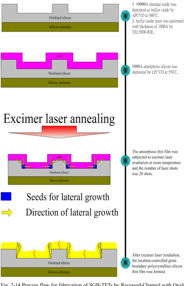
Fig. 2-14 Process flow for fabrication of SGB-TFTs by Recessed-Channel with Oxide Step method………...61
Fig. 2-15 The typical transfer characteristics of p-channel single gate LTPS-TFTs crystallized using Recessed-Channel with Oxide Step method. The channel length was 1 um. The laser energy was 560 mJ/cm2 and the number of laser shots was 20 (ie. 95% overlapping)………..64
Fig. 2-16 The output characteristics of p-channel single gate LTPS-TFTs crystallized using Recessed-Channel with Oxide Step method. The channel length was 1 um. The laser energy was 560 mJ/cm2 and the number of laser shots was 20 (ie. 95% overlapping)………64
Fig. 2-17 The typical transfer characteristics of p-channel single gate LTPS-TFTs crystallized using Recessed-Channel with Oxide Step method. The channel length was 1 um. The laser energy was 560 mJ/cm2 and the number of laser shots was 20 (ie. 95% overlapping)………...65
Fig. 2-18 The output characteristics of p-channel single gate LTPS-TFTs crystallized using Recessed-Channel with Oxide Step method. The channel length was 1 um. The laser energy was 560 mJ/cm2 and the number of laser shots was 20 (ie. 95% overlapping)………65
Fig. 2-19 SEM graph of the valley region of poly-Si thin film fabricated by Recessed-Channel with Oxide Step method……….66
Fig. 2-20 SEM graph of the ridge region of poly-Si thin film fabricated by Recessed-Channel with Oxide Step method……….66
Chapter 3
Fig. 3-1 SEM graph of ridge region of exceimer laser crystallized polycrystalline silicon by Recessed-Channel with Oxide Step method. The length of ridge region was 3 μm. The excimer laser energy density was 600 mJ/cm2……..67
Fig. 3-2 Process flow for fabrication of MG TFTs by Recessed-Channel with Oxide Step method………...68
Fig. 3-3 The typical transfer characteristics of SG-TFTs and MG-TFTs with location-controlled technology. The channel length was 1um. The laser energy was 560 mJ/cm2 and the number of laser shots was 20 (ie. 95% overlapping)………..71
Fig. 3-4 The output characteristics of SG-TFTs and MG-TFTs with location-controlled technology. The channel length was 1um. The laser energy was 560 mJ/cm2 and the number of laser shots was 20 (ie. 95% overlapping)………..71
Fig. 3-5 The typical transfer characteristics of SG-TFTs and MG-TFTs fabricated without location-controlled technology. The channel length was 1um. The laser energy was 560 mJ/cm2 and the number of laser shots was 20 (ie. 95% overlapping)………..72
location-controlled technology. The channel length was 1um. The laser energy was 560 mJ/cm2 and the number of laser shots was 20 (ie. 95% overlapping)………..72
Fig. 3-7 Field-effect mobility improvement of electrical characteristics of SG-TFTs and MG-TFTs with/without location-controlled grain boundary technology……….73
Fig. 3-8 Subthreshold swing improvement of electrical characteristics of SG-TFTs and MG-TFTs with/without location-controlled grain boundary technology……….73
Fig. 3-9 Threshold voltage improvement of electrical characteristics of SG-TFTs and MG-TFTs with/without location-controlled grain boundary technology…..74
Fig. 3-10 Leakage current improvement of electrical characteristics of SG-TFTs and MG-TFTs with/without location-controlled grain boundary technology…..74
Fig. 3-11 Field-effect mobility improvement of electrical characteristics of SG-TFTs and MG-TFTs with/without location-controlled grain boundary
technology……….75
Fig. 3-12 Subthreshold swing improvement of electrical characteristics of SG-TFTs and MG-TFTs with/without location-controlled grain boundary technology……….75
Fig. 3-13 Threshold voltage improvement of electrical characteristics of SG-TFTs and MG-TFTs with/without location-controlled grain boundary technology…..76
Fig. 3-14 Leakage current improvement of electrical characteristics of SG-TFTs and MG-TFTs with/without location-controlled grain boundary technology…..76
Fig. 3-15 The typical transfer characteristics of MG-TFTs fabricated by Recessed-Channel with Oxide Step method and conventional TFTs. The channel length was 1 um. The laser energy was 560 mJ/cm2 and the number of laser shots was 20 (ie. 95% overlapping)……….77
Fig. 3-16 The typical transfer characteristics of MG-TFTs fabricated by Recessed-Channel with Oxide Step method and conventional TFTs.. The channel length was 2 um. The laser energy was 560 mJ/cm2 and the number of laser shots was 20 (ie. 95% overlapping)………..77
Fig. 3-17 The typical transfer characteristics of MG-TFTs fabricated by Recessed-Channel with Oxide Step method and conventional TFTs.. The channel length was 3 um. The laser energy was 560 mJ/cm2 and the number of laser shots was 20 (ie. 95% overlapping)………..78
Fig. 3-18 The output characteristics of MG-TFTs fabricated by Recessed-Channel with Oxide Step method and conventional TFTs. The channel length was 1um. The laser energy was 560 mJ/cm2 and the number of laser shots was 20 (ie. 95% overlapping)………78
Fig. 3-19 The output characteristics of MG-TFTs fabricated by Recessed-Channel with Oxide Step method and conventional TFTs. The channel length was 2 um. The laser energy was 560 mJ/cm2 and the number of laser shots was 20 (ie. 95% overlapping)………79
Fig. 3-20 The output characteristics of MG-TFTs fabricated by Recessed-Channel with Oxide Step method and conventional TFTs. The channel length was 3 um. The laser energy was 560 mJ/cm2 and the number of laser shots was 20 (ie. 95% overlapping)………..79
Fig. 3-21 Statistics and uniformity of equivalent field effect mobility. Twenty p-channel MG-TFTs crystallized by Recessed-Channel with Oxide Step method and conventional MG-TFTs were measured. The laser energy was 560 mJ/cm2, the number of laser shots was 20(ie. 95% overlapping)……80
Fig. 3-22 Statistics and uniformity of threshold voltage. Twenty p-channel MG-TFTs crystallized by Recessed-Channel with Oxide Step method and conventional MG-TFTs were measured. The laser energy was 560 mJ/cm2, the number of laser shots was 20(ie. 95% overlapping)……….80
Fig. 3-23 Statistics and uniformity of subthreshold swing. Twenty p-channel MG-TFTs crystallized by Recessed-Channel with Oxide Step method and conventional MG-TFTs were measured. The laser energy was 560 mJ/cm2, the number of laser shots was 20(ie. 95% overlapping)……….81
Chapter 1
Introduction
1.1 Overview of Low-Temperature Polystalline
Silicon (LTPS) Thin Film Transistors (TFTs)
Recently, thin film transistors (TFTs) have become important devices in large area electronics system applications in the past ten years, including active-matrix liquid crystal displays (AMLCDs) and active matrix organic light emitting displays (AMOLEDs) [1.1]-[1.5].
Amorphous silicon thin film transistors (a-Si:H TFTs) were introduced in the 1970’s, which have been used in many applications such as solar cells [1.6], image sensors, printing heads, electronic copiers [1.7]-[1.9], especially in the applications of AMLCDs [1.10]-[1.12] and newly developed AMOLEDs [1.13]-[1.15]. In the AMLCDs, a-Si:H TFTs is used as the pixel switch placed at each pixel for addressing. While in the AMOLEDs applications, a-Si:H TFTs is used as the active device to provide driving current for illumination. Amorphous silicon TFTs exhibit low leakage current because of their high off-state resistivity. In addition, they are compatible with
large glass substrate for low process temperature. However, the electrical characteristics of a-Si TFTs such as carrier mobility (typically below 1 cm2/V-s) are inadequate for peripheral circuits . That is, additional integrated circuits (ICs) are needed to support the function of gate drivers and source drivers to drive a display panel. This will lead to high cost and poor reliability.
Polycrystalline silicon (poly-Si) was used to be the active material of TFTs for achieving higher performance in the 1980s. The effective carrier mobility in polycrystalline silicon was significantly higher (by two orders of magnitude) than those in amorphous silicon, so that both n- and p-channel TFTs with reasonably high currents could be achieved in polycrystalline silicon [1.16]. The capability to complementary metal-oxide-semiconductor (CMOS) circuits allows low-power driving circuitry to be integrated with the active matrix. The integration of both the active matrix pixel switching elements and the peripheral driving circuitry onto a single glass substrate, thus substantially reducing manufacturing complexity and cost. Therefore, LTPS TFTs have been investigated to achieve the goal of integrating peripheral circuit in a single panel, which is known as system on panel (SOP)
1.2 Overview of Crystallization of Amorphous
Silicon Thin Films
The crystallinity of poly-Si thin film has great influence on the performance of poly-Si TFTs because the poly-Si thin film act as the channel region in the poly-Si TFTs. Therefore, a crystallization method was very important for LTPS poly-Si TFTs. For a poly-Si thin film, the grain boundary cause a lot of defects, which is called strained bonds and dangling bonds. These defects act as trap states within the band gap and will degrade the electrical characteristics of poly-Si TFTs, such as carrier
mobility, threshold voltage, subthreshold swing, and the leakage current. It is believed that poly-Si thin film could obtain less defects by enlarging the grain size. Further, it was important to control the grain size ,the orientation of the grains, and the location of the grains to fabricate high quality poly-Si thin films. There are several ways to make the amorphous silicon thin film be re-crystallized into polystalline silicon thin film by additional energy, including solid phase crystallization, metal induced crystallization, and laser irradiation crystallization. These methods have some differences between them and will be introduced in the following three sections.
1.2.1 Solid Phase Crystallization of Amorphous Silicon Thin
Films
The solid phase crystallization (SPC) method is which the a-Si thin film can be re-crystallized to polystalline silicon thin film by thermal annealing. The maximum temperature in the SPC method is below 600℃ in order to compatible with glass substrate, the a-Si thin film is deposited at 550℃ using silane (SiH4), and the
following the SPC process, and the process temperature is kept at 600℃ in N2
ambient, whereas the process time is about 24 hours [1.17]-[1.18].
The grain size of solid phase crystallized poly-Si thin film is several times larger than that of as-deposited poly-Si thin film. Besides, the surface morphology is much smoother in SPC poly-Si thin film than in as-doped ones. However, the SPC TFTs suffers a lot of intra-granular defects and result in a bad performance. The most important of all is the fact that the annealing time is too long and this will limit the throughput to fabricate poly-Si thin film.
1.2.2 Metal Induced Crystallization of Amorphous Silicon
Thin Films
The metal induced crystallization (MIC) method is which inducing certain metals during the SPC process. The SPC’s process annealing temperature of amorphous silicon could be lowered (<500℃) and process duration could be reduced (<5hrs). The higher throughput will be obtained. Several metals have been proposed to be applied to MIC process, such as aluminum (Al), aurum (Au), nickel (Ni), platinum (Pt). Among these metals, Ni has been shown to be the best candidate of metal induced crystallization method at low temperature for good performance polystalline silicon TFTs. When nickel was deposited on amorphous silicon, followed by thermal annealing, octahedral precipitates NiSi2 would be formed on amorphous silicon films.
Owing to the very small mismatch (0.4%) of crystal lattice constant between the <111> orientation faces of nickel silicide and crystalline silicon, the defects in crystal can be minimized [1.19]-[1.22].
However, because it is lower the SPC’s annealing temperature by the addition of certain metals, the MIC re-crystallization method suffers high leakage current and cannot be avoided from MIC process. The metal residues act as metal contamination and offer leakage path under carrier transportation.
1.2.3 Laser irradiation Crystallization of Amorphous Silicon
Thin Films
Laser crystallization process in fabrication silicon-on-insulator devices for microelectronics and thin-film transistors for displays has been receiving considerable attention [1.23]-[1.29]. Laser crystallization can produce large-grained poly-Si thin
researches of laser crystallization of amorphous silicon films for the preparation of poly-Si films for LTPS TFTs have been studied using various kinds of lasers techniques, such as CO2, Ar, Nd:YAG, Nd:YVO4, excimer, femtosecond lasers, and
etc [1.28]-[1.36]. Among these laser techniques, excimer laser annealing, to date, is the widely used method to prepare poly-Si thin films because of its high pulsed-laser power for large area glass substrate and the large absorption coefficient for a-Si in the UV light region (optical absorption coefficient > 106 cm-1) for no damage to glass substrate. According the mixture gas used in the laser tube, excimer laser radiation of output wavelengths between 157 – 351 nm (157, 193, 248, 308 and 351 nm for F2,
ArF, KrF, XeCl and XeF laser, respectively) by the transient high voltage discharge with a short pulse duration (full width of half maximum ~ tens of nanoseconds). The basic principle of excimer laser crystallization is the phase transformation of silicon thin film from amorphous to single-crystal material via melting the Si thin film within a very short time. Actually, the a-Si thin film is heated to the temperature of about 1200℃ during laser irradiation. However, the high temperatures are only persistent for tens of nanoseconds during laser pulse duration. In consequence, the introduction of thermal damage to the glass substrate and the thermal compaction problem are relaxed, which are serious issues in the solid phase crystallization. Another unique advantage of excimer lasers is the strong optical absorption of UV light in silicon. As a result, most of the incident laser energy is absorbed closed to the surface of the thin film without causing severe thermal strain on the substrate. The unique advantages of strong optical absorption of the UV light in silicon and short pulse duration of the excimer laser imply that high temperature can be produced in the silicon surface region, causing rapidly melting and solidifying quickly, without significant heating the substrate and impurities contamination form the substrate diffusion into the silicon thin film. This technology yield high quality and large-grained poly-Si thin film for
high-performance LTPS TFTs on glass or plastic substrate with high throughput. Owing to the advantageous features of excimer laser crystallation for large area microelectronics fabrication, many researches have been done to study the dynamics kinetics and transformation mechanisms of the laser crystallization of a-Si thin films. The characteristics of poly-Si thin film have been shown to be related to the process conditions of ELC, such as laser energy density, laser pulse duration, laser shot number per area, crystallization ambient, and substrate temperature [1.37]-[1.41]. Moreover, the initial status of a-Si precursor film, including a-Si film thickness, hydrogen content, and impurity content, has a profound effect on the properties of the resulting poly-Si film [1.41]-[1.44]. According to the reports of James. S. Im et al., excimer laser crystallization of amorphous silicon thin films on foreign substrate can be divide into three transformation regimes with respect to the applied laser energy densities [1.45]-[1.46]. These are the partial-melting, full-melting, and near-chomplete-melting regimes.
Partial-melting regime (Low energy density regime)
In the partial melting regime, the incident laser energy density is larger than the threshold energy of melting of a-Si films the applied laser energy density can cause only surface melting of a-Si thin films but not the entire silicon films (i.e., melting deptn < film thickness). Therefore, a-Si thin film can be partially melted and subsequently be recrystallized from the underlying continuous layer of remained solid Si. In this regime, the poly-Si grain size increases with the increases of the laser energy density. In addition, it is characterized that explosive crystallization of a-Si thin film occurs at the onset of the transformation and follows by vertical grain growth, and competitive occlusion of grains [1.47]. The early trigger of explosive
presence of impurities in the silicon films.
Complete-melting regime (High energy density regime)
In the complete melting regime, the incident laser energy density is sufficient high to cause the complete melting of the entire a-Si thin films. Since the glass substrate is amorphous structure, epitaxial layer growth from the substrate is not possible. For the complete-melting Si thin film, a deep suercooling of the liquid silicon film leads to homogeneous nucleation before the transformation of poly-Si in solid phase [1.48]-[1.49]. In this regime, the final microstructure is insensitive to the applied laser energy densities. Fine-grained and small-grained poly-Si thin films are attained due to the low substrate temperature. In addition, a phenomenon of amorphization is observed in thinner silicon films [1.50].
Near-complete-melting regime (Super-lateral-growth regime)
In the near-complete-melting regime, the incident laser energy density leads to a complete melting a-Si thin film consisting of un-melted discrete silicon islands (i.e. melting depth ≈ film thickness). James. S. Im et al. identified the third transformation regime, the end of the low energy density regime and the beginning of the high energy density rgime, in a narrow experimental window [1.45]-[1.46]. In this regime, large-grained poly-Si films with grain sizes many times larger than the film thickness are observed. Since the grain size is much larger than that in the other two transformation regimes, Im named it super lateral growth (SLG) regime due to its unique nature [1.46]. based on Im’s model, it is argued that the un-melted portion of the under lying Si no longer forms a continuous layer but instead consists of discrete solid silicon islands which are separated by small local regions in the completely melting silicon film. The un-melted silicon islands act as nucleation seeds and lateral
grain growth can proceed toward the complete melting region. Therefore, a significant lateral growth takes place before the impingement of the grain grown from the other side depending on the separation distance between these seeds. There is a limit for the maximum lateral growth distance; however, since the continuous cooling of the liquid layer via thermal conduction to the underlying substrate eventually would leads to copious nucleation of solids in bulk liquid ahead of the interface. According to the SLG model, the super lateral grain growth distance will increase with thicker film thickness, higher substrate temperature, lower thermal conductivity of the substrate, and longer laser pulse duration. In addition, the applied energy density for super lateral growth regime increases with thicker film thickness, shorter laser pulse duration, higher thermal conductivity of the substrate, and lower substrate temperature. It is concluded that the lateral grain growth is resulted from the thermal gradient between the solid and liquid interface and the lateral grain growth distance is determined by the quenching rate of liquid silicon and the residual solid Si seed distance. As a result, the SLG distance can be prolonged by enlarging the lateral thermal gradient and increasing the solidification duration. However, a very non-uniform grain size distribution is observed in the SLG regime due to the fluctuation of pulse-to-pulse laser energy density, non-uniform laser beam profile, and non-uniformity of a-Si thin film thickness. The non-uniform grain distribution causes device degradation and poor device-to-device uniformity as the laser energy density is controlled in the SLG regime. It is very undesirable for device and circuits applications.
1.3 Ion activation
LDD, and source/drain regions must all be well activated. The energetic dopant ions cause significant damage to the silicon crystal structure near the surface regions during ion doping process. Activation is a thermal heating process to repair the lattice damaged regions into single-crystal structure and to activate the dopants. Only when the dopant atoms are at the single-crystal lattice sites can they provide electrons and holes as the majority carriers for device application. It has been reported that device with thinner active layer displays higher driving current, lower off-state leakage current, reduced kink current, and superior short channel characteristics. However, the high parasitic resistance of the thin source/drain regions degrades device performance such as effective field-effect mobility and driving current. In ULSI silicon semiconductor processing, activation is performed by either furnace annealing or rapid thermal processing (RTP) at temperature above 900℃. However, the maximum fabrication process temperature of LTPS TFTs is restricted to the softening point of glass substrate (~ 600℃). Activation poses a considerable challenge to LTPS TFTs producers owing to the temperature limitations. Because of the temperature restriction and the thin active layer, the high series resistance from source/drain regions will degrade device performance. In order to achieve low sheet resistance, the dopants in the source and drain regions must be activated to a high degree. The efficiency of the activation is dependent upon the doped impurities, activation temperatures and activation duration. Basically, activation methods used in LTPS TFT technology include furnace annealing, rapid thermal annealing, and laser annealing.
The most common approach of dopant activation is furnace annealing. This process is typically carried out at 600℃ for as long as tens of hours in nitrogen ambient. The long process time at low temperature is necessary in order to effectively activate the dopants while preventing the substrate free from warpage or damage. It is a technique of poor efficiency and low throughput for mass production.
Another concern for furnace annealing is the high thermal budget. The long-time furnace annealing process will cause severe dopant lateral diffusion which is intolerable for small geometrical transistors. Therefore, rapid thermal annealing (RTA) process is preferred for post-implantation annealing in the advanced fab. A RTA system can ramp up the temperature from room temperature to 900℃ in a very short time, typically within 10 seconds. The RTA process can precisely control temperature uniformity of the substrate and within substrate. At about 750℃, the single-crystal structure can be recovered and the dopant atoms will move to locate substitutional sites in about 1 second, with minimum lateral dopant diffusion. By processing at high temperatures while minimizing substrate damage, short process times, lower cost and high throughput can be achieved via RTA.
Since RTA method will also cause deformation of the glass substrate, laser annealing is the best candidate for dopant activation without substrate damage. Laser annealing process, the silicon is heated, melted and re-crystallized without heating the substrate, can achieve the highest activation efficiency compared to the other methods. Despite the high efficiency, some damages to device may occur during laser irradiation, such as the gate metal damage. In addition, throughput may be another potential bottleneck to the mass production.
1.4 Motivation
The low temperature polycrystalline silicon (LTPS) thin film transistors (TFTs) have been widely applied to high-definition active matrix liquid crystal displays (AMLCDs) and active matrix organic light emitting displays (AMOLEDs). The quality of the polycrystalline silicon thin film acts as the active layer of the devices plays an important role in the device to influence the electric characteristics greatly. In
order to fabricate a high performance LTPS TFTs, we introduce several aspects to improve the electrical characteristics of the LTPS TFTs: to reduce the defects of polycrystalline silicon thin, to raise the gate ability, and suppress the leakage current. The defects in the inter-grain will make the electrical characteristics of the device low, as reduce the carrier mobility and raise the leakage current of the device. In addition, the interface between the gate insulator and the active layer will influence the gate control ability. Form the views of reducing the defect of the polycrystalline silicon thin film, we introduced a simple method to fabricate the high quality polycrystalline silicon thin film, which is so called recessed-channel with oxide step structure. We also propose the multi-gate structure to enhance the gate control ability.
1.4.1 Fabrication of Polycrystalline Silicon Thin Film with
Location-Controlled Grain Boundary Technology
Among the various crystallization technologies for preparing polycrystalline silicon thin films, excimer laser crystallization (ELC) is the most promising technology to produce high quality polycrystalline silicon thin films on forein substrates at low temperature. Although pulsed excimer laser crystallization had the potential to improve the crystallinity of polycrystalline silicon thin films, narrow excimer laser crystallization process window, the uniformity and serious roughness of the crystallized polycrystalline silicon thin films were important issues. The excimer laser energy should be kept at a certain threshold value to make the amorphous silicon thin films which without laser irradiation is nearly completely melted, which is so called “super lateral growth” (SLG) regime; that is, excimer laser crystallization suffer narrow process window. In addition, the shot-to-shot laser energy of excimer laser crystallization is not stable enough and the seeds of crystallization distribute
randomly during laser re-crystallization. The excimer laser crystallization come out to a poor device-to-device uniformity.
For the purpose of the issues mentioned above, many laser crystallization technologies have been proposed to produce large grains with uniformly grain size distribution, including sequential lateral solidification (SLS) [1.51]-[1.52], grain filters method [1.53], capping the reflective or anti-reflective layer [1.54], phase-modulated ELC [1.55], dual beam ELA [1.56], double-pulsed laser annealing
[1.57]-[1.58], selectively floating a-Si active layer [1.59], continuous-wave laser lateral crystallization [1.60]-[1.61], selectively enlarging laser crystallization
[1.62]-[1.63], and so on. However, these methods are not compatible with the existing excimer laser annealing system or need complex process flows. Therefore, a simple method to control the direction of grain growth and the location of grain boundary has been developed in the thesis, which is called “Recessed-Channel with Oxide Step Method”. In this method, we can artificially control the thermal gradient in selective region, which is the step region and valley region, formed by pre-pattern buffer oxide step structure. The amorphous silicon thin film at the corner of oxide step region is thicker than elsewhere of the other region. If the laser energy density is controlled to completely melt the thinner region and partially melt the thicker region, a lateral thermal gradient will determine the grain growth from the un-melting solid phase seeds towards the melting liquid phase region. For the whole thesis, the crystallization is based on the structure.
1.4.2 Polycrystalline Silicon Thin Film Transistors with
Oxide Step Process
It has been demonstrated that the performance of devices can be enhanced with multi gate structure. Many kinds of gate structure, including double gates, dual-gates, tri-gate, Ω-gate, T-gate, and surrounding gate…etc. [1.64]-[1.68], are concentrated on the extension of the field induced device channel region. We could obtain better gate control ability and steeper Subthreshold swing than that of conventional single top gate structure. Among the gate structures mentioned above, the multi gate structure is adopted in this due to the compatibility with the location-controlled technology we propose. At first, we fabricate the polycrystalline silicon thin film by Recessed-Channel with Oxide Step method. There is a single grain boundary located in device channel region. After that, we use multi gate method to reduce the influence of main grain boundary.
1.5 Thesis Organization
In chapter 1, an overview of LTPS TFTs technology was given. The polycrystalline silicon crystallization process and ion activation process were brief explain. The motivations of this thesis were explained to introduce this thesis subsequently.
In chapter 2, experimental processes of elevated channel thin films were introduced. The mechanism of lateral growth of thin films fabricated by Recessed-Channel with Oxide Step method was proposed by material analysis. The material properties were analyzed by scanning electron microscope (SEM) and atomic force microscope (AFM). Then experimental procedures of polycrystalline silicon thin-film transistors fabricated by Recessed-Channel with Oxide Step structure were introduced. The electrical characteristics, including the field-effect mobility, the
subthreshold swing, and the threshold voltage were investigated by using Agilent 4156 system.
In Chapter 3. With a view to reduce the influence of main grain boundary located in device channel region, the MG-TFTs were fabricated by Recessed-Channel with Oxide Step method. The process flows and the grain boundary influence would be discussed in detail. The electrical characteristics of MG-TFTs, including the field-effect mobility, the subthreshold swing, the threshold voltage, and the uniformity were investigated.
Chapter 2
Fabrication of Location-Controlled
Single-Grain-Boundary (SGB)
Polycrystalline Silicon (Poly-Si) Thin
Film Transistors (TFTs) by
Recessed-Channel with Oxide Step
Methods Using Excimer Laser
Annealing (ELA)
2.1 Introduction
2.1.1 Introduction to Recessed-Channel with Oxide Step
Methods
Recently, Low-temperature Polycrystalline Silicon (LTPS) technology has been the most promising method to fabricate the high performance thin-film transistors (TFTs). High driving-current capacity, low leakage-current, and good uniformity are the characteristics of TFTs and those are imperative for devices aiming at the
application of AMLCD, AMOLED, and 3-dimensional ICs [2.1]-[2.6]. In comparison with amorphous silicon (a-Si) TFTs, the electric characteristics of polycrystalline silicon (poly-Si) TFTs is better than that of a-Si TFTs. Higher driving-current of LTPS TFTs due to the mobility of poly-Si TFTs was generally much higher than that of a-Si TFTs. The high driving-current make LTPS TFTs to act as pixel switching devices which are very small in size. In addition, LTPS TFTs are compatible with complementary metal-oxide-semiconductor (CMOS) circuits and allow the low-power accessional driver circuitry to be integrated within the active matrix circuit on a single substrate for the goal of system on panel (SOP), due to the better reliability and low power consumption of LTPS TFTs. As comparison with high temperature polycrystalline silicon (HTPS) TFTs, the LTPS TFTs technology was compatible with glass substrate even plastic substrate because the thermal budget was much lower for HTPS TFTs, and the cost of LTPS TFTs technology is much lower than that of HTPS TFTs in large panel application.
For preparing the LTPS thin films, several ways have been reported to date, including solid phase crystallization (SPC), metal induced lateral crystallization (MILC), and laser annealing [2.7]-[2.10]. The excimer laser annealing (ELA) method was most commendable to prepare the high quality of LTPS thin films. The excimer laser emits in UV light region with short pulse duration (10-30ns) by the laser source of ArF, KrF, or XeCl (output wavelengths 193, 248, and 308nm, respectively) gas source. The strong optical absorption of UV light and small diffusion length during the laser pulse in silicon imply that high temperature can be produced and cause melting of silicon without significant damage of glass substrates [2.11]. Besides, ELA poly-Si films have good crystallinity and few intra-grain defects due to the melt-regrowth process. The mechanism of grain growth during ELA process is quite
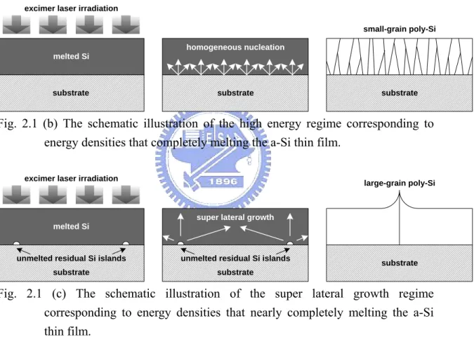
corresponding to the different laser energy densities. As shown in Fig. 2-1 (a), if the laser energy is controlled to melt the part thickness of a-Si thin film, vertical solidification occurs and the un-melted solid layer remains to be a-Si, while the melted Si layer transforms into poly-Si with small grain size [2.12]. Refer to Fig. 2-1 (b), if the laser energy density is high enough to completely melt the a-Si thin film, homogeneous nucleation occurs for deep supercooling to form small grain size [2.13]. Only when the laser energy density is controlled around a certain threshold value that leads to larger grain size, it is as large as 1μm in diameter, as shown in Fig. 2-1 (c). This is so called Super Lateral Growth (SLG) regime [2.14], which illustrates the behavior of melted a-Si to recrystallize from very few un-melted a-Si residues to each other. The very few residues act as the grain growth seeds, the lateral growth phenomenon causes large grain size.
The LTPS thin film fabricated by ELA technology showed good crystallinity with very few intra-grain defects and large grain. But the conventional ELA LTPS TFTs have some failings. The high surface roughness between active layer and gate insulator is due to the ridges formation between grain boundaries. Besides, the location of grain boundaries cannot be controlled due to the random position of nucleation by excimer laser crystallization, and many small grains still spread between these large grains in the super lateral growth (SLG) regime. A lot of process fluctuation factors exist, i.e., the pulse-to-pulse variation of excimer laser energy, the variation of a-Si film thickness, and the narrow process window with ELA process.
Many crystallization methods have been proposed to solve the above problems. They includes sequential lateral solidification (SLS) [2.15]-[2.22], grain-filters (or substrate-embedded seeds) method [2.23]-[2.25], phase-modulated ELC using an optical phase-shift mask [2.26]-[2.30], capping reflective or anti-reflective layer
pre-patterned a-Si thin film [2.42]-[ 2.45], dual beam ELA [2.46], and so on. Although all of them provided alternatives to produce large grain poly-Si thin films, however, most of them were not a simple solution for the fabrication of LTPS TFTs.
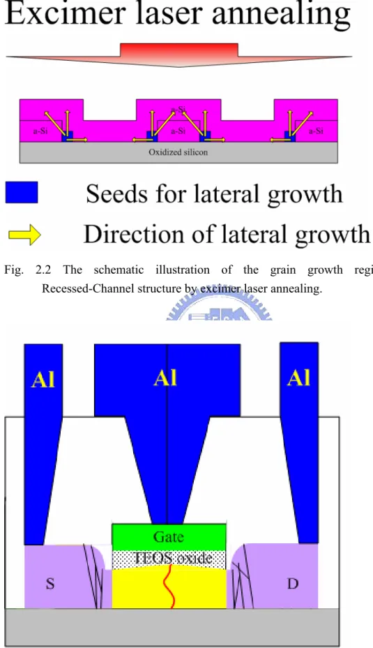
A novel and simple crystallization method to control lateral grain growth in the desired region was using excimer laser irradiation, called Recessed-Channel method.
Fig. 2-2 schematically illustrates the grain growth regime of the Recessed-Channel structure. In this method, a-Si thin film with two kinds of thicknesses in a local region was utilized for excimer laser irradiation. As a proper laser energy density was applied on the a-Si thin film, in which the thin part of a-Si was completely melted, a large lateral thermal gradient would exist between the complete melting silicon and partial melting silicon, and the grains would grow laterally from the un-melting solid silicon seeds in the thick part of a-Si towards the thin region where the silicon was completely melted. As a result, large and uniform longitudinal grains could be artificially produced in the desired local region.
As the principle of crystallization was applied to the fabrication of low temperature polycrystalline silicon thin film transistors, the thick part of a-Si was always served as the source/drain region, while the thin part of a-Si was served as the channel region, as shown in Fig. 2-3. Therefore, the large and uniform longitudinal grains could be formed in the channel region.
Although the poly-Si thin film with recessed-channel structure method had been successfully used to fabricate the large grain with high quality poly-Si thin film and the high performance ELA poly-Si TFTs, the location-controlled lateral growth grains would be obtained in the thin part of the ELA poly-Si thin film with Recessed-Channel method and the channel region of the device were in-situ designed in the thin part of the poly-Si thin film only. There were many small grains in the
of the amorphous silicon could not be full-melted during the excimer laser irradiation. The poly-Si TFTs would have poor electrical characteristics due to the small grains if the channel region of the TFTs was designed in the thick part of the ELA poly-Si thin film with Recessed-Channel structure. In order to obtain high performance poly-Si TFTs, the channel region of the TFTs must be designed to avoid the thick part of the ELA poly-Si thin film with the Recessed-Channel structure.
A novel method was carried out to improve the electrical characteristics of the ELA poly-Si thin film transistors with Recessed-Channel structure, namely Recessed-Channel with Oxide Step method. In this method, the buffer oxide thin film was patterned like the Recessed-Channel structure by excimer laser irradiation. According to the crystallization mechanism of excimer laser irradiation, we expected that the thick silicon in the corner of the oxide steps acted as the grain growth seeds during excimer laser irradiation. The grain boundaries with location-controlled distributed not only in the valley region (the thin part of the buffer oxide layer) but also in the step region (the thick part of the buffer oxide layer), and the uniformity of the devices will be improved. The drawback of the ELA poly-Si thin film with Recessed-Channel method can be excluded. Moreover, we obtained much larger process window rather than that of conventional whole flat thin film by ELA process.
Comparing with the Recessed-Channel method, the poly-Si thin film fabricated by Recessed-Channel with Oxide Step method will not need more than one additional amorphous silicon thin film deposition. The buffer oxide layer is formed as Recessed-Channel structure directly. The cost of the fabrication of the ELA poly-Si thin film fabricated by Recessed-Channel with Oxide Step method will be lower than that of Recessed-Channel method. Fig. 2-4 shows the diagrams of the Recessed-Channel method and the Recessed-Channel with Oxide Step method.
Step Process would be introduced. We studied the mechanism of lateral growth of Recessed-Channel with Oxide Step Process by material analysis equipments. The material properties of elevated channel thin films were investigated by scanning electron microscope (SEM) and atomic force microscope (AFM)..
2.2 Material Analysis of Location-Control Single
Grain Boundary Polycrystalline Thin Films
Fabricated by Recessed-Channel with Oxide
Step Method
2.2.1 Process Flows for Material Analyses of
Location-Controlled SGB Poly-Si Thin Film by
Recessed-Channel with Oxide Step Method
Detailed process flow of preparing samples was shown in Fig. 2-5. At first, a thermal oxide layer with thickness of 10000Å were deposited as buffer oxide layer by atmospheric pressure chemical vapor deposition (APCVD) at 980℃. Then, the buffer oxide layer was defined as period step with thickness of 1000Å by TEL5000-RIE. Next, a 1000 Å amorphous silicon thin film was deposited as the active layer by low pressure chemical vapor deposition (LPCVD) at 550℃ with SiH4 as gas source. The
Recessed-Channel with Oxide Step method was named as the first buffer oxide layer was pattern before buffer oxide layer deposited. Laser crystallization was performed using KrF excimer laser (λ = 248nm) in a vacuum chamber pumped down to 10-3 torr.
maintained at room temperature. The number of laser shots per area was 20 (i.e., 95% overlapping) and laser energy density was varied. The grain structure of the crystallized polycrystalline silicon thin film was analyzed using scanning electron microscope (SEM), atomic force microscopy (AFM) and transmission electron microscope (TEM). In order to facilitate the SEM observation, all the samples were processed by secco-etch before SEM analysis.
2.2.2 Material Analysis of Location-Controlled SGB Poly-Si
Thin Film by Recessed-Channel with Oxide Step
Method
Fig. 2-6 shows the diagram of the Recessed-Channel with Oxide Step structure. We defined the region where is the concave of the buffer oxide layer was called “valley region” and the region where was between the two valley regions was called “ridge region”. The thickness of the buffer oxide layer under the a-Si thin film in the valley region was 9000Å, and the thickness of the buffer oxide layer under the a-Si thin film in the ridge region was 10000Å. The length definition of the valley region and ridge region according to the buffer oxide layer patterned mask designed. We deposited the thermal oxide layer with thickness of 10000 Å on silicon substrate in order to simulate the quartz substrate.
2.2.2.1 Scanning Electron Microscope (SEM) Analysis
Fig. 2-7 shows SEM graphs of excimer laser crystallized polycrystalline silicon thin film in the thin part of the buffer oxide was 9000Å (valley region) by Recessed-Channel with Oxide Step method. The length between the steps was (a) 1.5μm and (b) 2 μm, respectively. The excimer laser energy was 540 mJ/cm2 and the
substrate temperature was maintained at room temperature during the excimer laser irradiation. The longitudinal grains with 1 μm were formed in the valley region. It has been reported that lateral thermal gradient could arise as a result of the heat generated at moving solid-melting interface [2.47]. When a controlled laser energy density irradiated the amorphous silicon thin film on the buffer oxide layer which containing different thicknesses, the valley region was completely melted while the thick part in the corner due to the poly-Si thin film fabricated by Recessed-Channel with Oxide Step method was only partially melted, leaving behind islands of solid material. As a result, grains would grow laterally towards the complete melting region from the retained solid seeds. The lateral growth would start from the solid amorphous silicon spacer seeds and stretch toward the completely melted region until the solid-melt interface from opposite direction collided. Due to the in-situ design of thin film transistors at the valley region, the grain boundaries perpendicular to the current flow in the valley region could be reduced. Thus the field-effect mobility of polycrystalline silicon TFTs could be greatly improved with this crystallization technique.
Comparison with the valley region of the polycrystalline silicon thin films with Recessed-Channel with Oxide Step method by excimer laser annealing, the surface morphology at the thick part of the buffer oxide layer with the thickness was 10000Å (ridge region) was observation by SEM analysis. Fig. 2-8 shows the SEM graphs of grain morphology of the ridge region of excimer laser crystallized polycrystalline silicon thin film by Recessed-Channel with Oxide Step method. The length of the oxide ridge was (a) 1.5μm and (b) 2μm, respectively. The excimer laser energy was 480 mJ/cm2 and the substrate temperature was maintained at room temperature during the excimer laser irradiation. The longitudinal grains with 0.75 μm were formed in the ridge region. The amorphous silicon thin film at step region would be completely
the buffer oxide steps would be partially melted. The silicon thin film at the corner region had more thermal energy than the silicon in the middle of ridge region due to the silicon thin film at the corner region had more vacuum space than the silicon in the middle of ridge region. As a result, grain growth would come up from the residual, un-melted silicon islands in the corner of ridge-valley structure and in the middle of ridge, and then grain growth must toward opposite direction. The grains grown from the corner with step structure and the middle of ridge region toward opposite direction due to the action of the vertical expanded solid material on the remaining (denser) liquid material. When two opposite freezing of capillary waves (maybe two or more grains) met, there was a grain boundary formation.
The laser influence determined the extension of lateral grain growth. When a longer channel was adopted for crystallization, the laser influence had to increase high enough to make the longitudinal grains collide with those grown from the other side; otherwise, small grains caused by spontaneous homogeneous nucleation would form in the center of the ridge region. Fig. 2-9 shows the SEM graphs of the ridge region of crystallized polycrystalline silicon thin film. The length of the ridge region was kept at 2 μm, and the excimer laser was varied different laser energy density. The substrate temperature was maintained at room temperature during the excimer laser irradiation. The longitudinal grains were still not long enough to collide with those grown from the other side. If spontaneous nucleation could be suppressed or delayed by substrate heating or any other methods to make the substrate keep the thermal energy, the lateral growth would enlarge to a longer distance and produce longer lateral growth. As a result, a suitable length of adjacent channel length, location control lateral grain growth could be acquired in the polycrystalline silicon thin film.
With a view to investigate the process window of the valley region fabrication by Recessed-Channel with Oxide Step method, we altered the laser energy density
irradiated on amorphous silicon thin film. Fig. 2-10 shows SEM graphs of the valley region and ridge region of poly-Si thin films with different laser energy densities while the length between the steps was kept at 2 μm. The laser energy density was increased from 520 mJ/cm2 to 600 mJ/cm2 and the substrate temperature was maintained at room temperature during the excimer laser irradiation. We concluded that the process window of Recessed-Channel with Oxide Step method is much larger than that of conventional excimer laser annealing on whole flat amorphous silicon thin film.
The grain lateral growth phenomenon happened not only in the valley region but also in the ridge region of the poly-Si thin film by Recessed-Channel with Oxide Step process. Therefore, the crystallinity of the ridge region of poly-Si thin film was determined by laser influence. The laser process window of the ridge region fabrication of poly-Si thin film with Recessed-Channel with Oxide Step process is investigated. Fig. 2-11 shows SEM graphs of the ridge region of poly-Si thin film by Recessed-Channel with Oxide Step process with different excimer laser energy densities. The length of the oxide ridge was 1.5μm and the substrate was maintained at room temperature during excimer laser irradiation. The excimer laser density was increased from 460 mJ/cm2 to 600 mJ/cm2. The excimer laser process window of the Recessed-Channel with Oxide Step method is large and easy to control.
2.2.2.2 Atomic Force Microscope (AFM) Analysis
By using AFM analysis the grains could be distinguished apparently due to the hung hillock formation at the grain boundaries. The hillock was resulted from the freezing of capillary waves excited in the melting silicon during excimer laser crystallization [2.48]. Grain boundaries and vertices which typically were the laser to freeze during lateral grain growth, had accumulated silicon due to the action of the
expanded solid material on the remaining (denser) liquid material. When the excimer laser crystallization began, nucleated grains advanced laterally through the denser liquid at first. As the solid regions grew, they filled a larger volume than the melt they consume. Eventually, the remaining liquid extended above the surrounding film. Where two grains met to form a grain boundary, a ridge developed. Where three or more grains met to form a vertex, a hillock might develop. As shown in Fig. 2-12, the length of the valley region was 2 μm and the excimer laser energy density was 600 mJ/cm2. The longitudinal grains with 1.5μm in length were formed in the excimer laser annealing silicon thin film of valley region. The roughness analysis was carried out at the valley region. The roughness of valley region of the thin film carried out by Recessed-Channel with Oxide Step method was smaller than the whole flat ELA thin films. Fig. 2-13 shows the AFM graph of the ridge region of poly-Si thin film with Recessed-Channel with Oxide Step method. The longitudinal grains with 0.75μm in length were formed in the excimer laser annealing silicon thin film of the ridge region. The roughness analysis at the ridge region was also shown the same smooth with the one of valley region. There were many small grains at the corner was rough due to the excimer laser energy was not full-melting the amorphous silicon where the silicon in the corner was thicker than the other.
2.3 Fabrication and Electrical Characteristics
Analysis of Location-Controlled
Single-Grain-Boundary (SGB)
Polycrystalline Silicon (Poly-Si) Thin-Film
Recessed-Channel with Oxide Step Method
2.3.1 Process Flow of SGB-TFTs by Recessed-Channel with
Oxide Step method
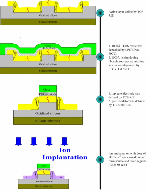
More detailed process flows of device fabrication were shown in Fig. 2-14. At first, the thermal oxide layer with thickness of 10000Å were deposited by atmospheric pressure chemical vapor deposition (APCVD) at 980℃ with hydrogen and oxygen as gas source. Then, the buffer oxide layer was defined as period step by TEL5000-RIE. Next, a 1000 Å amorphous silicon thin film was deposited as the active layer by LPCVD at 550℃ with SiH4 as gas source. The period step pre-pattern
oxide method was named as the first buffer oxide layer and was pattern before amorphous silicon layer deposited. Laser crystallization was performed using KrF excimer laser (λ = 248nm) in a vacuum chamber pumped down to 10-3 torr. During the laser irradiation, the samples were located on a substrate which is maintained at room temperature. The number of laser shots per area was 20 (i.e., 95% overlapping) and laser energy density was varied. Next, the active region was defined by TCP-RIE. Then, a 1000 Å TEOS oxide layer was deposited as top gate insulator by LPCVD at 700℃ followed by in-situ doping phosphorus polycrystalline silicon layer as top gate electrode. The top gate electrode was defined by TCP-RIE, and gate insulator was defined by TEL5000-RIE. Next, a BF2 ion implantation with a dosage of 5×1015 cm-2
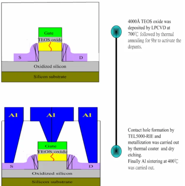
and energy of 50 keV was performed to form source and drain regions. A 4000 Å TEOS oxide layer was then deposited as passivation layer by LPCVD at 700℃ and the implanted dopants were activated by thermal annealing in furnace at 600°C for 9 hours. Then contact hole opening by TEL5000-RIE and metallization with Aluminum