metal-organic chemical vapor deposition
Yen-Chin Huang, Zhen-Yu Li, Li-Wei Weng, Wu-Yih Uen, Shan-Ming Lan, Sen-Mao Liao, Tai-Yuan Lin, Yu-Hsiang Huang, Jian-Wen Chen, Tsun-Neng Yang, and Chin-Chen Chiang
Citation: Journal of Vacuum Science & Technology A 27, 1260 (2009); doi: 10.1116/1.3212895 View online: http://dx.doi.org/10.1116/1.3212895
View Table of Contents: http://scitation.aip.org/content/avs/journal/jvsta/27/6?ver=pdfcov Published by the AVS: Science & Technology of Materials, Interfaces, and Processing
Articles you may be interested in
n -type, p -type and semi-insulating ZnO:N thin film growth by metal organic chemical vapor deposition with N H 3 doping
J. Vac. Sci. Technol. B 27, 1904 (2009); 10.1116/1.3151829
Effect of growth temperature on the characteristics of ZnO films grown on Si(111) substrates by metal-organic chemical vapor deposition
J. Vac. Sci. Technol. A 26, 224 (2008); 10.1116/1.2835090
Evolution of the electrical and structural properties during the growth of Al doped ZnO films by remote plasma-enhanced metalorganic chemical vapor deposition
J. Appl. Phys. 102, 043709 (2007); 10.1063/1.2772569
Raman and photoluminescence of ZnO films deposited on Si (111) using low-pressure metalorganic chemical vapor deposition
J. Vac. Sci. Technol. A 21, 979 (2003); 10.1116/1.1580836
Transparent and conductive Ga-doped ZnO films grown by low pressure metal organic chemical vapor deposition
„111… prepared by
atmospheric pressure metal-organic chemical vapor deposition
Yen-Chin Huang
Department of Electronic Engineering, College of Electrical Engineering and Computer Science, Chung Yuan Christian University, Chung-Li 32023, Taiwan
Zhen-Yu Li
Department of Photonics and Institute of Electro-Optical Engineering, National Chiao Tung University, 1001 TA Hsueh Road, Hsinchu 30010, Taiwan
Li-Wei Weng, Wu-Yih Uen,a兲Shan-Ming Lan, and Sen-Mao Liao
Department of Electronic Engineering, College of Electrical Engineering and Computer Science, Chung Yuan Christian University, Chung-Li 32023, Taiwan
Tai-Yuan Lin
Institute of Optoelectronic Sciences, National Taiwan Ocean University, Keelung 222, Taiwan
Yu-Hsiang Huang, Jian-Wen Chen, Tsun-Neng Yang, and Chin-Chen Chiangb兲
Institute of Nuclear Energy Research, P.O. Box 3-11, Lungtan 32500, Taiwan
共Received 7 July 2009; accepted 3 August 2009; published 14 September 2009兲
Gallium-doped ZnO films were grown on p-Si共111兲 substrates by atmospheric pressure
metal-organic chemical vapor deposition 共AP-MOCVD兲 using diethylzinc and water as reactant
gases and triethyl gallium 共TEG兲 as a n-type dopant gas. The structural, electrical, and optical properties of ZnO:Ga films obtained by varying the flow rate of TEG from 0.56 to 3.35mol/min were examined. X-ray diffraction patterns and scanning electron microscopy images indicated that Ga doping plays a role in forming microstructures in ZnO films. A flat surface with a predominant
orientation 共101兲 was obtained for the ZnO:Ga film fabricated at a flow rate of TEG
= 2.79mol/min. This film also revealed a lowest resistivity of 4.54⫻10−4⍀ cm, as measured
using the van der Pauw method. Moreover, low temperature photoluminescence 共PL兲 emission
recorded at 12 K demonstrated the Burstein Moss shift of PL line from 3.365 to 3.403 eV and a line
broadening from 100 to 165 meV as the TEG flow rate varied from 0.56 to 2.79mol/min. This
blueshift behavior of PL spectra from ZnO:Ga films features the degeneracy of semiconductor, which helps to recognize the enhancing of transparency and conductivity of ZnO films fabricated by AP-MOCVD using Ga-doping technique. © 2009 American Vacuum Society.
关DOI: 10.1116/1.3212895兴
I. INTRODUCTION
Zinc oxide共ZnO兲 is a wide band gap semiconductor with
a direct band gap of 3.37 eV at room temperature. It demon-strates high thermal and chemical stability, good electrical conductivity, and high optical transparency. In addition, it has a large exciton bind energy of 60 meV, which is 2.4 times larger than that of GaN. ZnO is extensively studied because of its potential applications in widespread fields, such as a transparent conductive layer and/or an
antireflec-tion coating for amorphous-silicon 共a-Si兲 and
Cu共InGa兲Se2-based solar cells.1–3Moreover, ultraviolet light
emitting devices4and laser diodes5based on this material are also possible. Undoped ZnO films usually show n-type con-ductivity but with a high resistivity due to the intrinsic de-fects of oxygen vacancies and zinc interstitials.6 Therefore, high conductive films can be obtained only by doping metal elements that substitute zinc sites.7,8 Compared to undoped
ZnO, the doped one has a lower resistivity and better stabil-ity of electrical properties. It is well known that group III elements such as Al,9 In,10 Ga,11 and B 共Ref. 12兲 act as
donors in ZnO. Among these metal dopants, Ga seems to be a promising one because the covalent bond length of Ga–O 共0.192 nm兲 is slightly smaller than that of Zn–O 共0.197 nm兲 and only small ZnO lattice deformations are caused even high concentrations of Ga are introduced.
For the deposition of Ga-doped ZnO 共ZnO:Ga兲 films, a
number of growth techniques such as, magnetron
sputtering,13–15 pulsed laser deposition,16,17 molecular beam epitaxy,18 atmospheric pressure metal-organic chemical
va-por deposition 共AP-MOCVD兲,19 plasma enhanced
metal-organic chemical vapor deposition,20 and low-pressure
metal-organic chemical vapor deposition21,22were used. In our study, we fabricate ZnO:Ga films by AP-MOCVD. Little has been known about the growth of ZnO:Ga film by this method. As is known, AP-MOCVD is a simple fabrica-tion process and cost competitive for device applicafabrica-tions of thin films. It is capable of producing high growth rates over large areas. Doped films can be deposited by introducing the
a兲Author to whom correspondence should be addressed; electronic mail
dopant into the gas phase, and the extent of doping can be easily controlled by the concentration of dopant in gas phase. We have recently reported the characterizations of absorption and transmission spectra of ZnO:Ga films fabricated on glass
substrates by AP-MOCVD.23ZnO:Ga films with a low
resis-tivity of 3.6⫻10−4⍀ cm and a high transparency of 85%
were achieved, which are expectable for being used as trans-parent electrodes in optoelectronic device applications. For a reference, TableIsummarizes some recent progress concern-ing the quality of ZnO:Ga films produced by MOCVD. In the present work, we report the characterizations of ZnO:Ga films fabricated on Si共111兲 substrate. The structural, electri-cal, and optical properties of ZnO:Ga films doped to different degrees were systematically examined to recognize the dop-ing capability of Ga elements in ZnO film and also the avail-ability of ZnO:Ga for a transparent conductive film. II. EXPERIMENTS
ZnO thin films were deposited using a custom-made
one-flow AP-MOCVD system. The substrates are 2 in.
共111兲-oriented, p-type Si wafers with a resistivity of 1 – 3 k⍀ cm. The growth chamber is a water-cooled vertical reactor. The substrate susceptor is made of graphite, 2 in. in diameter and coated with a SiC film on top surface by CVD technique.
Diethylzinc 共DEZn兲 and water were used as the sources of
Zn and O, respectively. Besides, triethyl gallium共TEG兲 was used as the doping gas for Ga. N2was used as the carrier gas for the growth of ZnO:Ga films. Before the ZnO:Ga film growth, an undoped ZnO buffer layer of about 5 – 10 nm was grown at a low temperature of 200 ° C and with a gas flow
ratio of 关H2O兴: 关DEZn兴 共VI/II ratio兲=6.84. Then, the
growths of ZnO:Ga top layers were conducted at 400 ° C with their VI/II ratios being kept at 1.37 and growth time duration set for 30 min to achieve a thickness of about 200– 300 nm. Specimens for comparison were fabricated
with different TEG flow rates ranging from
0.56 to 3.35mol/min for Ga doping.
The crystalline structure of the ZnO:Ga thin films was
analyzed by powder x-ray diffraction 共XRD兲 共Bruker AXS
Diffraktometer D8兲 using Cu K␣ line as the x-ray source
共=1.540 56 Å兲. The surface morphology and thickness of ZnO films were examined by a scanning electron microscope 共SEM兲 共JEOL-6700F兲 at an accelerating voltage of 10 kV. The resistivity, carrier concentration, and mobility of films were measured at room temperature by Hall measurements
using the van der Pauw method. The optical properties were
characterized by photoluminescence共PL兲 measurements
per-formed at 12 K. PL spectra were excited with the 325 nm line of a He–Cd laser.
III. RESULTS AND DISCUSSION
Figure1shows the XRD patterns of ZnO:Ga film
depos-ited on p-Si共111兲 substrate under the TEG flow rate of 0.56– 3.35mol/min. As can be seen from Fig. 1, all the films exhibit grain structures with a preferential orientation
of 共101兲 accompanied by a weak 共002兲 peak. This result is
quite different from those conventionally investigated, such
as that reported in Ref. 26 where heavily Ga-doped films
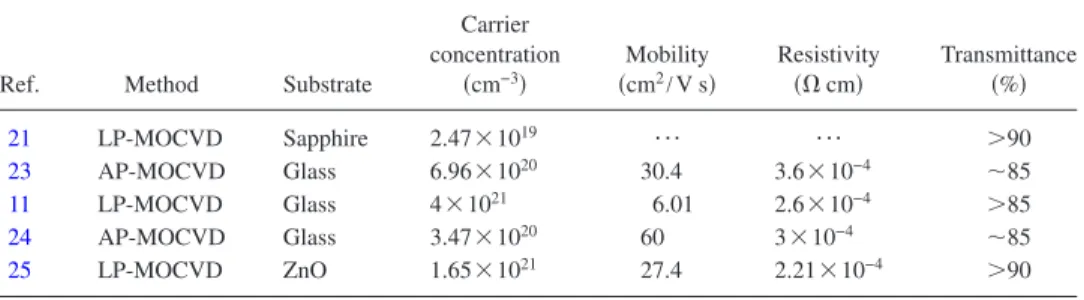
were examined. The共101兲 peak retains its intensity while the 共002兲 peak gets weaker decreases with increasing the TEG flow rate to 2.79mol/min and somehow regains its inten-sity again with a further increase in TEG flow rate to TABLEI. Summary of the progress in ZnO:Ga films produced by MOCVD.
Ref. Method Substrate
Carrier concentration 共cm−3兲 Mobility 共cm2/V s兲 Resistivity 共⍀ cm兲 Transmittance 共%兲 21 LP-MOCVD Sapphire 2.47⫻1019 ¯ ¯ ⬎90 23 AP-MOCVD Glass 6.96⫻1020 30.4 3.6⫻10−4 ⬃85 11 LP-MOCVD Glass 4⫻1021 6.01 2.6⫻10−4 ⬎85 24 AP-MOCVD Glass 3.47⫻1020 60 3⫻10−4 ⬃85 25 LP-MOCVD ZnO 1.65⫻1021 27.4 2.21⫻10−4 ⬎90
FIG. 1. XRD patterns of ZnO:Ga films fabricated with different TEG flow rates.
3.35mol/min. The results described above imply that the Ga elements involved in ZnO film would influence the grain formation therein. Although it is suggested in Ref.26that the Ga doping causes the grains to grow without any predomi-nant direction, in the present study the Ga doping was found to dominate the film growth with the appearance of兵101¯1其 planes on top. Different results presented above are probably due to the different methods used for growing ZnO:Ga, how-ever, further studies must be conducted to clarify the details. The SEM surface images of ZnO:Ga thin films fabricated with various TEG flow rates are shown in Figs. 2共a兲–2共e兲. Also, the cross-sectional images of these films are shown in the respective inset of these figures. It is obvious that ZnO:Ga films fabricated with the TEG flow rates ranging
from 0.56 to 1.68mol/min exhibit surface morphologies
full of irregular grain structures. Those grains can be roughly categorized into the larger ones and the smaller ones accord-ing to their sizes, which have made the whole film surfaces become very rugged. However, a more homogeneous forma-tion of grains is observable when the TEG flow rate is in-creased to 2.23mol/min as demonstrated in Fig. 2共d兲 and the corresponding inset. In particular, as exhibited in Figs.
2共e兲and2共f兲, the ZnO:Ga films fabricated with a TEG flow
rate over 2.79mol/min show relatively uniform grain
structures and their cross-sectional SEM images manifest the top surface of these films to be very flat compared to those
grown with the TEG flow rates lower than 2.23mol/min.
Analogous results have been found on heavily Ga-doped films evaluated by atomic force microscopy and explained by modeling the grain formation considering the Ga-doping effect.27It is noticeable that the film surface changes from an irregular structure to homogeneous morphologies with an
in-crease in TEG flow rate to over 2.23mol/min and
there-fore the grain boundaries are also believed to be simulta-neously reduced.
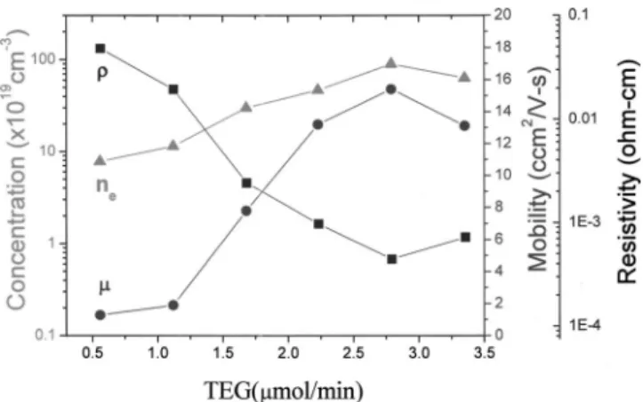
Figure 3 displays the resistivity 共兲, electron concentra-tion共ne兲, and Hall mobility 共H兲 of ZnO:Ga films as a
func-tion of the TEG flow rate. The undoped ZnO shows p-type conductivity, with,H, and hole concentration measured as
0.7516⍀ cm, 42.1 cm2V−1s−1, and 1.97⫻1017cm−3, re-spectively. As known, the intrinsic conductivity of ZnO is greatly influenced by the point defects produced therein. The
p-type conductivity of undoped ZnO has been reported to be
possibly due to the formation of Zn vacancies.28On the other hand, Ga is a n-type dopant that replaces zinc atoms共GaZn兲
or forms interstitial atom共Gai兲 in ZnO, which increases the
free electron concentration in the films. It can be seen that the resistivity of ZnO:Ga thin film decreases initially with increasing TEG flow rate and achieves a minimum value of
4.54⫻10−4⍀ cm at the TEG flow rate=2.79mol/min.
Then it increases conversely with a further increase in TEG flow rate. Whereas, the electron concentration increases
gradually with increasing TEG flow rates from
0.56 to 2.79mol/min and reaches a maximum value of
8.93⫻1020cm−3. However, a further increase in TEG flow
rate to 3.35mol/min makes the electron concentration re-duce to 6.28⫻1020cm−3. Obviously, the Ga atoms in the
films have a tendency to occupy interstitial sites as neutral defect, and even substitute oxygen site as an acceptor at higher doping concentrations, which is responsible for the decrease in electron concentration when the TEG flow rate is increased to 3.35mol/min. This carrier compensation phe-nomenon was also observed by Hu et al.19for ZnO:Ga layers at high doping level. Moreover, the Hall mobility initially increases with the TEG flow rate and begins to decrease after
a maximum value of 15.4 cm2V−1s−1 is achieved at the
TEG flow rate= 2.79mol/min. As is reported, the Hall mo-bility共H兲 can be expressed as29
FIG. 2. SEM top-view images of ZnO:Ga films deposited with different TEG flow rates: 共a兲 0.56, 共b兲 1.12, 共c兲 1.68, 共d兲 2.23, 共e兲2.79, and 共f兲 3.35mol/min. The inset of each figure shows the corresponding cross-sectional image.
FIG. 3. Resistivity, electron concentration, and mobility of ZnO:Ga films deposited with various TEG flow rates.
1 H = 1 i + 1 g ,
where i and g are the mobilities dominated by impurity
scattering and grain boundary scattering, respectively. i
should decrease with increasing TEG flow rate since the amount of Ga atoms incorporated in ZnO film is increased. Hence, it is reasonable to consider that the increase in H
with increasing TEG flow is mainly dominated by g. As
demonstrated in both XRD and SEM results described above, the grain structure is simplified and exhibits a rela-tively flat surface as the TEG flow rate is increased to over 2.79mol/min. This should be connected to a reduction in the area of grain boundaries, which should have been ben-eficial for elevatinggand thereforeH. That is to say, the
increase in Hall mobility is due to the reduction in scattering from the grain boundaries. However, a further raise of TEG
flow rate to 3.35mol/min might enhance the Ga-related
donor impurity, acceptor impurity, and/or defect scatterings to reducei, which would result in loweringH, too.
Figure4shows PL spectra of undoped and Ga-doped ZnO
films measured at 12 K. As can be seen, the PL spectrum of undoped ZnO displays several emission lines near ZnO band edge, such as 3.357, 3.309, 3.240, and 3.169 eV. The emis-sion line at 3.357 eV is attributed to the recombination of excitons bound to neutral acceptors30or those bound to neu-tral donors.31The strongest emission line at 3.309 eV is as-signed to the donor-acceptor pair recombinations,
accompa-nied by two LO-phonon replicas at 3.240 eV 共1-LO兲 and
3.169 eV共2-LO兲.32In contrast, the PL spectrum of Ga-doped ZnO film fabricated with a TEG flow rate of 0.56mol/min is dominated by the emissions at 3.365 and 3.333 eV, which are related to the excitons bound to neutral donors.33
Finally, for the film fabricated with a TEG flow rate of 2.79mol/min, the excitonic emission seems to be embed-ded in a wide band-to-band transition with a blueshift of the emission peak to 3.403 eV. No visible emissions are discov-ered for all PL spectra. This implies that the doping of Ga elements into the ZnO lattice does not bring about the de-fects responsible for deep level related emissions.21The ori-gins of the blueshift and linewidth broading for the PL emis-sion of heavily doped films are further analyzed below.
Figure 5 shows 共a兲 the normalized PL spectra measured at
12 K and共b兲 the peak position and full width at half
maxi-mum共FWHM兲 of ZnO:Ga films fabricated with various TEG
flow rates ranging from 0.56 to 3.35mol/min. As the TEG
flow rate increases from 0.56 to 2.79mol/min, the PL
peak also shifts from 3.365 to 3.403 eV and meanwhile the
FWHM of PL spectrum also increases from
100 to 165 meV. Two plausible mechanisms are considered to be responsible for the blueshift and linewidth broadening of PL spectra related to the well-known Burstein–Moss effect.34,35The origin of this effect is the shift of the Fermi level 共EF兲 to above the bottom of the conduction band 共Ec兲
as the doping degree surpasses the degeneracy limit. Thus, the peak position of PL spectra shifts to higher energies fol-lowing Fermi level, as described by the equation below,36
EF− Ec=
ប2
2me*共3
2n兲2/3, 共1兲
where n represents the net electron concentration, ប the re-duced Planck constant, and me* the effective electron mass. Furthermore, due to indirect transitions 共violating the k se-lection rule兲 between the filled states in the conduction band and valence band, the FWHM of PL was found empirically to increase with the energy shift.37The indirect character of such transitions was ascribed to the scattering of carriers by ionized donors and Auger processes.38Otherwise, some pre-vious reports indicated a clear redshift due to the band tailing effect for their PL spectra of ZnO:Ga films.8,18,21 Such a variation in PL spectra is interpreted as mainly due to a band gap narrowing caused by impurity-induced potential fluctua-tion. However, the related redshift behavior was ultimately not observed through all our measurements compared to the energy gap of an intrinsic material. Even the specimen fab-ricated with the TEG flow rate high to 3.35mol/min just exhibited a slight decrease in the PL peak energy to 3.393 eV due to the compensation effect of electrons.
IV. CONCLUSIONS
Characterizations of ZnO:Ga films fabricated on
p-Si共111兲 substrates by AP-MOCVD using TEG as the
dop-ing gas have been systematically conducted. It was found that the amount of Ga elements doped in ZnO film evidently influence its grain structure, electrical, and optical properties. For the range of TEG flow rate investigated, a flat surface with the predominant orientation of共101兲 can be obtained for the ZnO:Ga films fabricated at the TEG flow rate over
2.79mol/min. Moreover, the TEG flow rates higher than
2.23mol/min can be used to obtain ZnO:Ga films with low FIG. 4. PL spectra of undoped and Ga-doped ZnO films measured at 12 K.
resistivity values 共10−3– 10−4⍀ cm兲. In particular, the film
fabricated at the TEG flow rate= 2.79mol/min revealed
simultaneously a highest electron concentration of 8.93 ⫻1020cm−3, a highest Hall mobility of 15.4 cm2V−s−1, and
also a lowest resistivity of 4.54⫻10−4⍀ cm. The mobility is
considered to be dominated by the grain boundary scattering when the TEG flow rate is lower than 2.79mol/min, but is dominated by the ionized impurity scattering when the TEG
flow rate is higher than 2.79mol/min. This phenomenon
has made a highest mobility be achieved at the TEG flow rate= 2.79mol/min. In addition, a compensation effect is suggested to explain the decrease in electron concentration after the maximum value is obtained. Combining both the variations of electron concentration and mobility as a func-tion of the TEG flow rate naturally yields a lowest resistivity at the TEG flow rate= 2.79mol/min. Conclusively, degen-erate n-type ZnO films can be produced by AP-MOCVD using the Ga-doping technique, which is further character-ized by the blueshift共3.365–3.403 eV兲 and linewidth
broad-ening 共100–165 meV兲 of PL spectra for the specimens
fab-ricated with various TEG flow rates共0.56–2.79mol/min兲.
1B. Rech and H. Wagner, Appl. Phys. A: Mater. Sci. Process. 69, 155
共1999兲.
2A. Shimizu, S. Chaisitsak, T. Sugiyama, A. Yamada, and M. Konagai,
Thin Solid Films 361–362, 193共2000兲.
3J. C. Lee, K. H. Kang, S. K. Kim, K. H. Yoon, I. J. Park, and J. Song, Sol.
Energy Mater. Sol. Cells 64, 185共2000兲.
4D. C. Look, Mater. Sci. Eng., B 80, 383共2001兲.
5S. J. Pearton, D. P. Norton, K. Ip, Y. W. Heo, and T. Steiner, Prog. Mater.
Sci. 50, 293共2005兲.
6A. F. Kohan, G. Ceder, D. Morgan, and C. G. Van de Walle, Phys. Rev. B
61, 15019共2000兲.
7K.-K. Kim, S. Niki, J.-Y. Oh, J.-O. Song, T.-Y. Seong, S.-T. Park, S.
Fujita, and S.-W. Kim, J. Appl. Phys. 97, 066103共2005兲.
8T. Makino, Y. Segawa, S. Yoshida, A. Tsukazaki, A. Ohtomo, and M.
Kawasaki, Appl. Phys. Lett. 85, 759共2004兲.
9T. Minami, H. Nanto, and S. Takata, Jpn. J. Appl. Phys., Part 2 23, L280
共1984兲.
10K. L. Chopra, S. Major, and D. K. Pandya, Thin Solid Films 102, 1
共1983兲.
11Y. Li, G. S. Tompa, S. Liang, C. Gorla, Y. Lu, and John Doyle, J. Vac. Sci.
Technol. A 15, 1063共1997兲.
12X. L. Chen, B. H. Xu, J. M. Xue, Y. Zhao, C. C. Wei, J. Sun, Y. Wang, X.
D. Zhang, and X. H. Geng, Thin Solid Films 515, 3753共2007兲.
13X. Yu, J. Ma, F. Ji, Y. Wang, X. Zhang, C. Cheng, and H. Ma, J. Cryst.
Growth 274, 474共2005兲.
14X. Yu, J. Mat, F. Ji, Y. Wang, X. Zhang, and H. Ma, Thin Solid Films
483, 296共2005兲.
15Q. B. Ma, Z. Z. Ye, H. P. He, S. H. Hu, J. R. Wang, L. P. Zhu, Y. Z.
Zhang, and B. H. Zhao, J. Cryst. Growth 304, 64共2007兲.
16Z. F. Liu, F. K. Shan, Y. X. Li, B. C. Shin, and Y. S. Yu, J. Cryst. Growth
259, 130共2003兲.
17S. J. Henley, M. N. R. Ashfold, and D. Cherns, Surf. Coat. Technol.
177–178, 271共2004兲.
18H. Kato, M. Sano, K. Miyamoto, and T. Yao, J. Cryst. Growth 237–239,
538共2002兲.
19J. Hu and R. G. Gordon, J. Appl. Phys. 72, 5381共1992兲.
20V. Khranovskyy, U. Grossner, V. Lazorenko, G. Lashkarev, B. G.
Svens-son, and R. Yakimova, Superlattices Microstruct. 39, 275共2006兲.
21J. D. Ye et al., J. Cryst. Growth 283, 279共2005兲.
22E. W. Forsythe, Yongli GaO, L. G. Provost, and G. S. Tompa, J. Vac. Sci.
Technol. A 17, 1761共1999兲.
23Y. C. Huang et al., Thin Solid Films 517, 5537共2009兲.
24B. Hahn, G. Heindel, E. Pschorr-Schoberer, and W. Gebhardt, Semicond.
Sci. Technol. 13, 788共1998兲.
25N. Nishimoto et al., J. Cryst. Growth 310, 5003共2008兲.
26O. Nakagawara, Y. Kishimoto, H. Seto, Y. Koshido, Y. Yoshino, and T.
Makino, Appl. Phys. Lett. 89, 091904共2006兲.
27V. Khranovskyy, U. Grossner, V. Lazorenko, G. Lashkarev, B. G.
Svens-son, and R. Yakimova, Thin Solid Films 515, 472共2006兲.
28Y. Ma et al., J. Appl. Phys. 95, 6268共2004兲.
29S. Ghosh, A. Sarkar, S. Chaudhuri, and A. K. Pal, Thin Solid Films 205,
64共1991兲.
30J. Gutowski, N. Presser, and I. Broser, Phys. Rev. B 38, 9746共1988兲. 31D. C. Reynolds, D. C. Look, and B. Jogai, Phys. Rev. B 57, 12151
共1998兲.
32B. P. Zhang, N. T. Binh, Y. Segawa, Y. Kashiwaba, and K. Haga, Appl.
Phys. Lett. 84, 586共2004兲.
33A. Teke, Ü. Özgür, S. Doğan, X. Gu, H. Morkoç, B. Nemeth, J. Nause,
and H. O. Everitt, Phys. Rev. B 70, 195207共2004兲.
34E. Burstein, Phys. Rev. 93, 632共1954兲.
35T. S. Moss, Proc. Phys. Soc. London, Sect. B 67, 775共1954兲. 36A. Walsh, J. L. F. D. Silva, and S. H. Wei, Phys. Rev. B 78, 075211
共2008兲.
37J. De-Sheng, Y. Makita, K. Ploog, and H. J. Queisser, J. Appl. Phys. 53,
999共1982兲.
38S. M. Ryvkin, Phys. Status Solidi 11, 285共1965兲.