國 立 交 通 大 學
電子工程學系 電子研究所碩士班
碩
士
論
文
考慮存在電壓島的緩衝器繞線樹架構的一個有效率的演算法
An Efficient Algorithm for Voltage Island Aware Buffered Routing
Tree Construction
研 究 生:曾柏欽
指導教授:陳宏明 博士
存在電壓島的緩衝器繞線樹架構的一個有效率的演算法
An Efficient Algorithm for Voltage Island Aware Buffered
Routing Tree Construction
研究生: 曾柏欽
Student: Bruce Tseng
指導教授: 陳宏明 博士 Advisor: Prof. Hung-Ming Chen
國 立 交 通 大 學
電子工程學系 電子研究所碩士班
碩士論文
A Thesis
Submitted to Department of Electronics Engineering & Institute of Electronics College of Electrical Engineering and Computer Science
National Chiao Tung University in Partial Fulfillment of Requirements
for the Degree of Master of Science
in
Electronics Engineering July 2006
Hsinchu, Taiwan, Republic of China
i
考慮存在電壓島的緩衝器繞線樹架構的一個有效率的演算法
研究生:曾柏欽 指導教授:陳宏明 博士
國立交通大學
電子工程學系 電子研究所碩士班
摘要
由於低功率的方法論在超大型積體電路(VLSI)和系統單晶片(SoC)的
需求,電壓島(voltage island)越來越吸引設計者的注意。然而,相對應
在電子自動化設計(EDA)工具方面,考慮到電壓島的繞線樹建構仍然非常
稀少。[7] 是第一個深入研究應用兩種不同 Vdd 電壓的緩衝器在繞線樹的
建構上,並且藉由限制緩衝器的擺放順序而忽略電壓轉換器(level
converter)需求的考量。然而,因為有這些限制,所以這個方法並不能應
用到具有電壓島的設計上面。
本篇論文提出一個演算法以解決具有電壓島的低功率設計上緩衝器
以及電壓轉換器放置的問題。既然[7](使用[9]中的技巧)無法應用在電壓
島的設計上,我們改進[9]中 RMP 的方法以適用在此種設計上。我們更進
一步的發展我們的方法來做比較。藉由一些貪婪探索(greedy heuristic)
的技巧,我們的方法不僅非常有效率,而且能維持解的品質。
ii
實驗結果顯示相較於改良的 RMP 方法,我們的方法是非常有效率,甚
至於會有較低的功率和延遲(delay)。再者,當汲點(sink)的個數增加,
改良的 RMP 方法無法在一合理的時間內找到一組解答,我們的方法可以更
有效率的找到一組適當的解。
iii
An Efficient Algorithm for Voltage Island Aware Buffered Routing
Tree Construction
Student: Bruce Tseng Advisor: Prof. Hung-Ming Chen
Department of Electronics Engineering
& Institute of Electronics
National Chiao Tung University
Abstract
Due to the need of low power methodology in VLSI and SoC designs,
voltage island architecture is attracting attentions in design community.
However, the corresponding EDA tools development regarding routing tree
construction is still very few. [7] is the first in-depth study on applying dual
Vdd buffers in routing tree construction, with the restriction on the ordering
of buffers and the lack of level converter consideration. However this
approach cannot be applied on a design with voltage islands due to these
restrictions.
This paper presents an algorithm to solve the buffer insertion and level
converter assignment problem in the presence of voltage island in a
low-power design. Since [7] (use techniques in [9]) cannot be performed on
voltage island designs, we have modified RMP approach in [9] to perform on
those designs. We then develop our approach for comparison. With some
greedy heuristics and prune techniques, our approach is very efficient and it
still keeps the quality of solutions.
The experimental results show that we can obtain massive speedup over
modified RMP approach, and even with lower power and delay. Furthermore,
as number of sink increases, modified RMP cannot find solutions within a
reasonable CPU time, while our approach can efficiently find feasible
solutions.
v
誌謝
首先要特別感謝的人,是我的指導教授陳宏明老師,帶領我進入一個新的領 域 EDA,感謝老師的指導與包容,讓我可以完成本篇論文並且學習到許多 EDA 相關的知識。 此外,要感謝的是 VDA LAB 實驗室所有的成員,兩年來相互的勉勵、幫忙, 一起歡樂,有壓力時相互扶持,讓我有兩年充實的生活。 家人對我的支持、鼓勵更是我研究路上最大的依靠,對他們的感謝,更是筆 墨難以形容。 最後由衷感謝所有幫助過、關懷過我的人,謝謝! 曾柏欽 民國九十五年七月 於新竹i
Contents
List of Figures ii List of Tables iv 1 Introduction 1 1.1 Previous Works . . . 21.1.1 Treed base bu¤er insertion algorithms . . . 3
1.1.2 Graph based bu¤er insertion algorithms . . . 3
1.1.3 DVB algorithm[7] . . . 4
1.2 Our Contributions . . . 6
1.3 Organization . . . 6
2 Preliminaries 7 2.1 Power and Delay Estimation Models . . . 7
2.2 Problem Formulation . . . 9
3 Modi…ed RMP algorithm 11 3.1 Construct Grid Graph . . . 11
3.2 Fill Initial Solutions . . . 12
3.3 Solution Propagation . . . 14
3.4 Solution Pruning . . . 16 4 Greedy Heuristic: Fast Voltage island Aware Bu¤ered Tree Construction(FVABT) 17 5 Experimental Results 23 6 Conclusion and Future Work 26 Bibliography 27
List of Figures
1.1 For a voltage island design, we always need level converter to maintain signal integrity. Our approach views level converter as a kind of bu¤er, and bu¤er insertion operation will place level converter at a better location than conven-tional tree based algorithm. . . 2 1.2 [2] uses a -model instead of Elmore delay model and changes the load
capac-itancecap in Van Ginneken’s original candidate as (Cn; R; Cf). . . 4
1.3 Refer from [7]. DVB algorithm states that to have the delay of case (b) larger than case (a), Cl must be larger than 0.5pF or an equivalent 9mm interconnect wire. Therefore, DVB algorithm restricts the bu¤ers ordering as case (b). . . 5 2.1 Power and delay model while a bu¤er drives a wire with lengthLand a
capac-itance load withCLOAD, where cw is unit length capacitance,rw is unit length
wire resistance, andRb is the output resistance for bu¤ers. . . 8
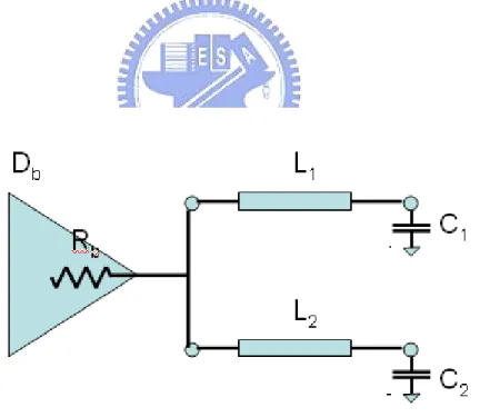
2.2 An example of delay computation: a bu¤er drives two wire segments L1, L2
with capacitance loadC1 and C2: . . . 8
3.1 Grid graph construction. We de…ne a bounding box that covers all the source, sink nodes and none of obstacles is cut by the bounding box. Then we partition the bounding box into a grid graph. . . 12 4.1 An example of performing FVABT to a net with 3 sink nodes, the yellow
circles are bu¤er locations. After generating the bu¤ered routing tree for t1, the solutions with rs = ft1g need to be kept for the node on the desired path
could be Steiner points while performing modi…ed RMP on next sink node. . . 19 4.2 Apply modi…ed RMP on sink node t2. Because of the former kept solution,
a bu¤ered routing tree with a shared path between source and node A could be generated. After performing modi…ed RMP tot2, solutions of nodes on the
desired path withrs = ft2g should be kept. Besides, solutions of nodes on the
desired path with rs = ft1; t2g should also be kept such that they can be used
(nodes as Steiner points) when the path is possibly shared by handling next sink. . . 20 4.3 After performing modi…ed RMP on sink node t3, if there exists another sink
which needs to be processed, the solutions that we demonstrate in this …gure should be kept. . . 21
iii 4.4 FVABT (Modi…ed RMP with greedy heuristic). Let modi…ed RMP only applies
on one sink. Once we process this sink, a desired solution is chosen, and the useless solutions are cleared in this grid graph. We keep on applying modi…ed RMP algorithm until all the sinks are processed. . . 22 5.1 The resultant bu¤ered routing tree of net5, which presents the case that a
source node is within the voltage island. The little squares are feasible bu¤er lcoations where none of bu¤er places there. The rectangle circled with dotted line is the voltage island. . . 24 5.2 The resultant bu¤ered routing tree of net6, which presents the case that a
List of Tables
5.1 Comparison between modi…ed RMP and FVABT algorithm. The results present advantages in both algorithms for casesnet4, net5, andnet6. However our ap-proach shows massive speedup over modi…ed RMP algorithm. For larger cases, modi…ed RMP cannot …nd solutions in six hours. . . 24
1
Chapter 1
Introduction
In CMOS digital circuits, power dissipation mainly consists of dynamic and static components. Dynamic and static power both have direct relationship with supply voltage Vdd. One of the techniques to reduce power consumption is voltage island methodology,
proposed from IBM [16]. A voltage island is a group of on-chip cores powered by the same voltage source, independently from the chip-level voltage supply. Voltage island architecture can achieve power saving and this technique becomes more and more popular [14]-[19].
Nevertheless, there are very few development in corresponding EDA tools regarding voltage-island-aware routing tree construction. Based on the state-of-the-art bu¤ered tree methodologies, we can put them into two categories. The …rst type is tree based algorithms [1]-[6]. They …rst generate routing tree topology, and use van Ginneken’s approach [1] to insert bu¤ers on this tree. The second type is graph based algorithms [7]-[13]. They deal with both routing and bu¤er insertion at the same time. Consider the circuit of a voltage island design, such as shown in Figure 1.1, we must use some level converters/shifters to maintain signal integrity when a low Vdd device drives a high Vdd device. If we use one of
the tree based algorithms to do the bu¤er insertion and level converter assignment, there will be two concerns. First, the generated routing tree may not have feasible level converter location. As a result, signal integrity will not be able to be kept. Second, if we regard level converter as a standard cell and place it during placement stage, signal integrity can be maintained though, the location of level converter will a¤ect total wirelength, delay and power. On the contrary, if we regard a level converter as a kind of bu¤er, a graph based algorithm will provide better solutions. But the complexity analysis in [9][10] has shown that graph based algorithms have a serious problem in exponential increase of runtime when
Level
shifter
High Vdd
Low Vdd
Figure 1.1: For a voltage island design, we always need level converter to maintain signal in-tegrity. Our approach views level converter as a kind of bu¤er, and bu¤er insertion operation will place level converter at a better location than conventional tree based algorithm.
the number of sinks increases. The experimental results shown in [7] also report the same observation.
1.1
Previous Works
Some algorithms about bu¤er insertion problem have been proposed in [1] -[13]. Some of these methods regard the routing tree as an input, and bu¤er insertion algorithm intends to …nd a minimum delay for this routing tree. Because the input of the algorithm is a tree, we classify these algorithms as tree based bu¤er insertion algorithms. On the other hand, others simultaneous bulid a routing tree and perform bu¤er insertion during buliding routing trees. Although these kinds of approaches always lead to less delay than tree based bu¤er insertion algorithms, most of these algorithms need to spend more time on computing
3
a better result. Because the algorithms always create a graph for bu¤er insertion, we classify these algorithm as graph based bu¤er insertion algorithms. Here we introduce some of algorithms to show the di¤erences. Then we describe the DVB algorithm in [7] for dual-Vdd
bu¤er insertion.
1.1.1 Treed base bu¤er insertion algorithms
Almost all the tree based algorithms are based on the algorithm proposed by van Ginneken[1]. van Ginneken’s algorithm deals with a routing tree which has multiple sinks and considers delay minimization only. It traverses a tree with a bottom up approach, and calculates delay with Elmore delay model during traversing a tree. For a tree withnfeasible bu¤er location and bu¤er library has only one bu¤er, there should be2nkinds of bu¤er tree. But in van Ginneken’s algorithm, a prune technique is adopted such that there will be only
nkinds of bu¤er tree and results in a time complexity of O(n2).
For 2 candidates (D1; C1); (D2; C2), where D states the accumlated delay and C states
the accumlated load capacitance. IfD1 > D2 andC1 > C2, then(D1; C1)can be pruned.
After [1] has proposed, some algorithms intends to model the delay more accurately, such as [2]. Just like we demonstrate in Figure 1.2, [2] uses a -model and changes the load capacitance part as (Cn; R; Cf). Besides, some of the papers, such as [3] [4] [5], use either
a balanced tree for storing the candidates or some aggressive pruning methods to make the algorithm even faster. Recently, [4] has improved the time complexity of a bu¤er insertion algorithm for a 2-pin net from O(n2) toO(nlogn); and toO(nlog2n) for multi-pin nets.
Because tree based algorithms regard routing tree as an input, the routing tree could not be changed during bu¤er insertion stage. And routing algorithms usually intends to …nd a Minumum Reclinear Steiner Tree (MRST) with minimum total wirelength. Therefore, if the routing tree has less feasible bu¤er locations, the bu¤er insertion algorithm can only improve the delay with these locations and will result in a poor delay while comparing with a graph based bu¤er insertion algorithm. Moreover, for a design with voltage island, if the MRST has none of feasible level converter location, the signal integrity can not be maintained and a large leakage current will be generated.
1.1.2 Graph based bu¤er insertion algorithms
Figure 1.2: [2] uses a -model instead of Elmore delay model and changes the load capacitance
capin Van Ginneken’s original candidate as (Cn; R; Cf).
bu¤er insertion and wire sizing problem as a theoretic shortest path problem in [13]. But it still needs to consume much time on solving both maze routing and bu¤er insertion problem for a multiple sink net. Such as [11] [12], the maze routing with bu¤er insertion problem is converted into a graph collection problem. Various kinds of bu¤er routing tree subsets are pre-computed as a table. And the bu¤er routing tree is constructed through a dynamic programming approach with combining these subsets. Although the dynamic programming approaches consume less time, their algorithms still need much time on table computation.
J. Cong et. al. proposed a RMP (Recursively Merging and pruning) algorithm in [9]. Di¤erent from [11] [12], RMP simultaneously bulids the routing topology with considering the bu¤er insertion at the same time. RMP …rst creates a grid graph and solutions with factors of capacitance cap, required arrival time RAT, reachable sink set RE and buf for stating whether a bu¤er which had been placed is …lled into each node in the created graph. With de…ning the formulation of solution propagation, various kind of solution could be generated during solution propagation. And each solution corresponds to a bu¤er routing tree. Therefore, various kinds of bu¤er routing tree is generated during computation, and the solutions at the source node states all the possible bu¤er trees.
1.1.3 DVB algorithm[7]
DVB algorithm which is the …rst in-depth study on applying dual Vdd bu¤ers to
5
Figure 1.3: Refer from [7]. DVB algorithm states that to have the delay of case (b) larger than case (a), Cl must be larger than 0.5pF or an equivalent 9mm interconnect wire. Therefore, DVB algorithm restricts the bu¤ers ordering as case (b).
could neglect the level converter. Their algorithm is realized with both tree based and graph based method. And the experimental result shows that their algorithm reduces 18~26% power consumption while comparing with using signal Vdd bu¤ers for bu¤er insertion. For DVB algorithm with graph based method, their algorithm is similiar to RMP algorithm. And a time consuming problem is also occurred in their experiment result. That is their algorithm needs more than 20 minutes to perform both routing and bu¤er insertion for a net with 6 sink.
For Figure 1.3, which DVB algorithm states that to have the delay of case (b) larger than case (a), they …nd that Cl must be larger than 0.5pF or an equivalentlly a
9mm interconnect wire. Therefore, they restrict bu¤er’s ordering by only high Vdd bu¤ers could drive a low Vdd bu¤ers, and thus none of level converter is needed in their algorithm. Alghough, this could reduce the complexity of a dual Vdd bu¤er insertion problem, but the assumption makes the algrotihm not realistical enough. First, for Figure 1.3 (b), if the sink device which Cl states is an high Vdd device, there will still need another level converter
between the low Vddbu¤er and Cl, or else a large leakage current occurs at sink device. Under
algorithm is applied on a design with dual Vdd voltage, and their algorithm inserts both low
and high Vdd bu¤ers anywhere in this design. It will make P/G line routing becomes a tough problem. Besides this, most dual Vdd design uses a voltage island ‡oorplan, and a level converter is widely used. Without considering the level converter, it makes the DVB algorithm becomes not realistical.
1.2
Our Contributions
To deal with this problem, we adopt prune technique and a greedy heuristic in the proposed algorithm FVABT (Fast Voltage island Aware Bu¤ered Tree construction). This algorithm uses a graph based algorithm to deal with both bu¤er insertion and level converter assignment problem, and also improves the time-consuming problem in graph based algorithm.To the best of our knowledge, this paper is the …rst work on the bu¤ered routing tree construction in the presense of voltage islands. The contributions presented in this paper are as follows:
Since current dual-Vdd bu¤er insertion approach cannot be performed on the designs with voltage islands, we have modi…ed the approach in [9] (RMP) so that it can be used with designs that contain voltage islands.
Our approach has obtained massive speedup over modi…ed RMP, and even produced lower power bu¤ered tree. Furthermore, as number of sink increases, our approach can …nd feasible solutions e¤ectively and e¢ ciently.
1.3
Organization
The rest of this paper is organized as follows. Section II introduces the power and delay estimation model used and problem formulation. Section III shows modi…ed RMP algorithm and Section IV introduces our greedy heuristic FVABT to apply on modi…ed RMP algorithm for runtime reduction. Section V shows our experimental results and Section VI concludes the paper.
7
Chapter 2
Preliminaries
We introduce the models that we use in this thesis, and formulate our problem as follows.
2.1
Power and Delay Estimation Models
We adopt the power and delay model introduced in [7]. The delay model is a distributed Elmore delay model. For the circuit shown in Figure 2.1, the delay of a wireDw
and delay of a bu¤erDbuf are de…ned as:
Dw(L) = (12 cw L + Cload) rw L
Dbuf= Db+Rb Cload
where cw is unit length capacitance, rw is unit length wire resistance, L is the downstream
wire length,Vdd is the voltage level of the device or the signal on the wire,Db is the instrinsic
delay of a bu¤er, Rb is the output resistance of a bu¤er, Cload is the downstream load
ca-pacitance.The interconnect power consumptionPw measured by energy per switch is de…ned
as:
Pw(L) =12 cw L V2dd
We give an example as follows to further illustrate our estimation model.
Example 1 For the circuit shown in Figure 2.2, a bu¤er drives two wire segments with
L1=100um,L2=200um, and the load capacitance on these two segments areC1=30fF,C2=40fF,
with the paramenters rw=0.186 /um, cw=0.0519fF/um, Db=72ps and Rb=4.7k . The
R
br
w*L
c
w*L
C
LOADFigure 2.1: Power and delay model while a bu¤er drives a wire with lengthLand a capacitance load withCLOAD, wherecw is unit length capacitance, rw is unit length wire resistance, and
Rb is the output resistance for bu¤ers.
Figure 2.2: An example of delay computation: a bu¤er drives two wire segmentsL1, L2 with
9
The delay due to a bu¤er:
Dbuf= Db+Rb(C1+L1cw+C2+L2 cw)
= 72 + 4:7 (30 + 100 0:0519 + 40 + 200 0:0519) = 474:179ps
The delay due to the wires:
Dw = max fDw(L1); Dw(L2)g
= max f(12 cw L1+C1) rwL1; (12 cwL2+C2) rw L2g
= max f606:267; 1681:068g = 1681:068ps
The total delay:
Dtot= Dbuf+Dw
= 474:179 + 1681:068 = 2155:247ps
2.2
Problem Formulation
Our problem is based on the following assumptions. There are two types of bu¤ers (bu¤ers with high and low Vdd) and one type of level converters with various kinds of size
in the bu¤er library, level converters must be drived by a high Vdd supply voltage so as to
raise voltage level from low to high. Hence both level converters and high Vdd bu¤ers can
only be placed within a high Vdd region, low Vdd bu¤ers can only be placed within low Vdd
region. Note that a voltage island might be turned o¤ while the chip is operating at power saving mode. The problem of bu¤er insertion and level converter assignment on a dual Vdd
voltage island design can be speci…ed as follows:
Problem 2 Given a design with voltage island(s), a net with a source node, multiple sink node with RAT (required arrival time) at each sink, feasible bu¤er location, bu¤er library and wire obstacles (such as hard IPs), we want to construct bu¤ered routing tree with bu¤er insertion and level converter assignment under the following constraints:
RAT at each sink should be met.
The design works during power saving mode, such that the bu¤ered routing tree has minimized power consumption.
11
Chapter 3
Modi…ed RMP algorithm
Since there are no approaches which can be used in routing tree construction for designs with voltage islands, we modify the original RMP in [9], which is used in [7], to …t a voltage island design, and try to speed up the algorithm as well. In order to …t a voltage island design, we use an indicator to show the possible voltage level of a signal(signalV )and keep on maintaining this indicator in this methodology.
Instead of fetching the solution with the maximal RAT among all the solutions, modi…ed RMP algorithm classi…es solutions with their reachable sinks, and store these so-lutions to a container called wave. A wave is popped and solutions of nodes in this wave are propagated to its neighboring nodes. The new generated solutions are also categorized with their reachable sinks, and these new solutions are stored in a new wave. During each iteration, if the new wave does not contain the source node, we store this new wave. If it contains the source node, this new wave is ignored. There are four steps in the modi…ed RMP algorithm, and the details of these modi…cations are shown in the following subsections.
3.1
Construct Grid Graph
First, we create bounding box with the minimum rectangle covering all the source and sink nodes. Then we keep on enlarging the bounding box such that there exists none of wire obstacles being cut. During box enlarging, if source node of the net is out of the voltage island, we also regard voltage island as an obstacle. We then partition the bounding box into a grid graph by using the vertical and horizontal line intersect at source and sink nodes, bu¤er locations, and four corners of the wire obstacle. An example of the grid graph
Figure 3.1: Grid graph construction. We de…ne a bounding box that covers all the source, sink nodes and none of obstacles is cut by the bounding box. Then we partition the bounding box into a grid graph.
is shown in Figure 3.1.
3.2
Fill Initial Solutions
During this step, we …ll initial solutions for each cross point in the grid graph. There are ten items (cap; rat; pow; rn; rs; B; signalV; Cbl; bend; totLength)in each solution, listed as follows:
cap: The accumulated capacitive load.
rat : Required arrival time.
pow : The accumulated power consumption.
rn(reachable node): The nodes that passed through to prevent from following the same path.
13 B: The location where a bu¤er is placed and the size of the bu¤er placed at this location.
signalV (signal voltage): Possible signal voltage level. If it is high, the solution can only be drived by a high Vdd device. If it is low, both high and low Vdd device can
drive this solution.
Cbl: When two solutions with di¤erent sink are merged at bu¤er location, Cbl states the extra load capacitance that the bu¤er needs to drive.
bend: The accumlated number of bendings in current solution. We use this to prune solutions.
totLength: The accumlated wire length.
According to the type of the node, one or some of the initial solutions are …lled for each node. The initial solution at sink node is the starting point for the propagation, while the solutions at the other nodes are formed through the propagation toward the source node. The rules for …lling the initial solution are described below. We assume that there are nH
high Vdd bu¤ers, nL low Vdd bu¤ers, m voltage level converters in the bu¤er library.
If node i is a sink node, …ll one solution:
(capi; rati; 0; fig; fig; ; signalVi; 0; 0; 0)
It states a bu¤ered routing sub-tree with zero wire length and it contains only the sink nodei. Thecapand ratstate the load capacitance and requirement arrival time of this sink iseparately.
If node i is a source node, …ll one solution:
(0; 1; 0; fig; ; bs; Low; 0; 0; 0)where bsinput capacitance=0, delay=0, output resistance=driving
resistance of source node.
It states a bu¤er with the driving resistamce of the device at source node is placed.
If node i is not a bu¤er location, …ll one solution:
(0; 1; 0; fig; ; ; Low; 0; 0; 0)
If node iis a bu¤er lcoation and within the voltage island (low Vdd region), …ll 1 + nL
solutions:
(0; 1; 0; fig; ; ; Low; 0; 0; 0);
(0; 1; 0; fig; ; b1L; Low; 0; 0; 0)~ (0; 1; 0; fig; ; bnL; Low; 0; 0; 0)
It states the case that none of bu¤er is placed or the cases for various kinds of low Vdd
bu¤er placed.
If node i is a bu¤er location and outside the voltage island, …ll 1 + nH+ m solutions:
(0; 1; 0; fig; ; ; Low; 0; 0; 0);
(0; 1; 0; fig; ; b1H; Low; 0; 0; 0)~ (0; 1; 0; fig; ; bnH; Low; 0; 0; 0);
(0; 1; 0; fig; ; b1; Low; 0; 0; 0)~ (0; 1; 0; fig; ; bm; Low; 0; 0; 0)
It states none of bu¤er is placed or the cases for various kinds of high Vdd bu¤er being
placed or the cases for various kinds of level converter being placed. Because some of the level converters needs both of the high and low Vdd voltage source and it easilier
for us to transfer a high Vdd to a low Vdd, we only allowed the converters placed at a
high Vdd region.
During …lling initial solutions, solution at each sink node is pushed into a container called wave separately. The solutions in the waves will be propagated in next step.
3.3
Solution Propagation
Here we choose a wavewin each iteration, and then propagate every solution within
w to neighboring nodes. While a solution sA at node A propagates to solution sB at the
neighboring node B, there are three conditions regarding voltage islands to follow:
If any sink voltage in s is high and source voltage is high, we cannot put any bu¤er within voltage island.
If signalV in sis high, the neighboring node cannot be placed low Vdd bu¤er.
15
Due to these conditions, we generate a new solutionsnew and store it in node B. We
also store the solution in a wave with itsrs. The new solution snew is:
If BB= (Node B does not place bu¤er):
capnew= capB+capA+CW
ratnew= min(ratB; ratA DW)
pownew= powA+powB+Pw
rnnew= rnA[rnB
rsnew= rsA[rsB
Bnew= BA[BB
signalVnew= signalVA Cblnew= 0
bendnew = bendA+ bendB+ ((turn direction)?1 : 0)
totLengthnew= totLengthA+ totLengthB+ (distance between A and B)
If BB 6= (Assume bu¤er j places at node B with output resistance Rj, delay Dj,
capacitanceCj)
capnew= Cj
ratnew= min(D1; D2); where D1 = ratB Rj (Cw+ capA); D2 = ratA (Dw+ DB+ Rj
Cblnew)
pownew = powA+ Pw(V dd based on driver) + PB
rnnew= rnA[rnB
rsnew= rsA[rsB
Bnew= BA[BB
SignalVnew= (BB is a level converter)?low : (VAjjVB)
bendnew = bendA+ bendB+ ((turn direction)?1 : 0)
totLengthnew= totLengthA+ totLengthB+ (distance between A and B)
3.4
Solution Pruning
In order to reduce runtime and the memory space usage, we have de…ned two prune conditions in modi…ed RMP algorithm. Assume that there are two solutions sA and sB
within the same node, we prefer to prune the solutions with more bends, and with power and capacitance dominance.
Prune with bends: If bendA> bendB; totLengthA totLengthB; ratA ratB, then sA is
dominated and can be pruned.
Prune with VG approach: If signalVA= signalVB; powA< powB; capA capB; ratA
17
Chapter 4
Greedy Heuristic: Fast Voltage island
Aware Bu¤ered Tree
Construction(FVABT)
Generally the modi…ed RMP algorithm deals with a net that has nsink nodes, and the grid graph has size N M and K solutions with the same rs need propagation in each node. Becausen sink node has 2n kinds of combinations, the modi…ed RMP algorithm has
O(2n N M K) solutions during propagation. It is obvious that computation time will increase expontentially as number of sink increase. If modi…ed RMP algorithm only process one sink at a time, the complexity can be reduced to O(N M K):
Rather than handling 2n kinds of sink combinations, FVABT performs modi…ed RMP algorithm with one sink only at each iteration. In other words, because the propagation allows to merge solutions with di¤erent sink at each node in the grid graph, the modi…ed RMP algorithm regards each node as a Steiner point. The solutions in the grid graph corresponding to various kinds of Steiner tree are generated. Instead of treating each node as a Steiner point, a desired solution is selected and then retrace the graph to erase the solutions that does not relate to the desired one. This approach can e¢ ciently reduce Steiner points.
FVABT algorithm performs modi…ed RMP algorithm for each sink, until all the sinks are handled. After one source-sink pair has …nished the execution of the modi…ed RMP algorithm, a desired lowest power solution is selected. Note that since the objective is low power, if we only keep the exact low power solution and prune others, in next iteration
modi…ed RMP algorithm may not merge the solution with the stored low power solution due to timing violation problem. Therefore, one of the major issues in FVABT is to keep the useful solutions in the grid graph. Assume that after performing modi…ed RMP to sink ti
and a desire solutionsolD has chosen. For each node in graph, the following solutions should
be kept while erasing solutions:
For every nodes in the graph, keep the initial solutions generated during …lling initial solution step.
Because the initial solutions are used such that a bu¤ered routing tree could be gen-erated at the source node, therefore, we need these initial solutions to generate the bu¤ered routing tree for next sink.
For nodes on the desired path that solD passed by, keeps solutions that rs = ftig and
solutions related with various kinds of bu¤er insertion on the desired path should be kept.
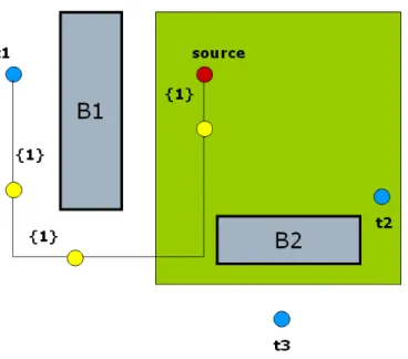
The reason of keeping these two kinds of solution is that we want to keep some Steiner points for next sink’s usage. Here, we use an example to explain. While performing FVABT for a net with 3 sink nodes, shown in Figure 4.1, t1 is …rst processed with
modi…ed RMP algorithm because it is nearest to source node. A desire path between source node and t1 is then select. The solutions of nodes on the desired path with
rs = ft1g are kept. The reason is that the nodes on the desired path could be Steiner
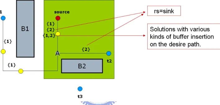
points while performing modi…ed RMP for next sink t2. While performing modi…ed
RMP fort2, shown in Figure 4.2,t2 could share with the former bu¤ered routing tree by
using node A as a Steiner point since solutions with rs = ft1g are kept at node A. After
performing modi…ed RMP on t2, solutions of nodes on the desired path with rs = ft2g
should be kept. Furthermore, solutions of nodes on the desired path with rs = ft1; t2g
should also be kept such that they can be used (nodes as Steiner points) when the path is possibly shared by handling next sink. Finally t3 is processed, if there exists another sink which needs to be processed, the useful solutions of the nodes on the desired path should be kept, shown in Figure 4.3.
The FVABT algorithm is shown in Figure 4.4. First, the waves in FVABT are di¤erent from the ones in the modi…ed RMP. In order to pop the desired wave with target
19
Figure 4.1: An example of performing FVABT to a net with 3 sink nodes, the yellow circles are bu¤er locations. After generating the bu¤ered routing tree for t1, the solutions with
rs = ft1g need to be kept for the node on the desired path could be Steiner points while
performing modi…ed RMP on next sink node.
sink nearest to source during each iteration, VABT only marks each wave with its target sink, while modi…ed RMP marks each wave as the solution’s reachable sinks of nodes within a wave. Therefore, solutions in a wave might have di¤erent reachable sinks in FVABT algorithm, but all these solutions are intended to bulid a tree for this target sink. After a wave with target sink nearest to source is fetched, solutions of nodes in this wave will be propagated to its neighbors with the solution propagation described in Section III.C (line 4-9). Once we have propagated one of its neighboring node, we prune the redundant new generated solutions and store the non-redundant solutions to the neighboring node. When one or more than one new generated solutions are stored, we store the neighbor to a temporary wave (line 10-14). Whenever we complete a wave propagation, we check whether source is visited. If visited, we choose a desired solution which has lowest power consumption and reach the target sink of this wave. If not visited, we again store the new generated wave (line 15-20). The program stops until all the sinks have been processed.
Figure 4.2: Apply modi…ed RMP on sink node t2. Because of the former kept solution, a
bu¤ered routing tree with a shared path between source and node A could be generated. After performing modi…ed RMP tot2, solutions of nodes on the desired path with rs = ft2g
should be kept. Besides, solutions of nodes on the desired path with rs = ft1; t2g should
also be kept such that they can be used (nodes as Steiner points) when the path is possibly shared by handling next sink.
21
Figure 4.3: After performing modi…ed RMP on sink node t3, if there exists another sink which needs to be processed, the solutions that we demonstrate in this …gure should be kept.
Figure 4.4: FVABT (Modi…ed RMP with greedy heuristic). Let modi…ed RMP only applies on one sink. Once we process this sink, a desired solution is chosen, and the useless solutions are cleared in this grid graph. We keep on applying modi…ed RMP algorithm until all the sinks are processed.
23
Chapter 5
Experimental Results
We have implemented modi…ed RMP and our heuristic in C++ and the platform is on AMD Dempron 1.75GHz with 1GB memory. We randomly generate several test cases. All these cases have six obstacles, one voltage island, and ten bu¤er feasible locations, but the number of sinks, pin location assignment, and bu¤er location assignment are di¤erent. For each of these cases, the size of the grid graph is about 25*25 on a 17*17mm design, and the number in each …le name shows the total number of source and sink pins.
The experimental results for modi…ed RMP and our heuristic are shown in Table 5.1. Since our heuristic performs the tradeo¤ in …nding solutions, the results present advantages in both algorithms for cases net4, net5, and net6. However our approach shows massive speedup over modi…ed RMP algorithm. Moreover, when the number of sink is larger than six, modi…ed RMP cannot …nd solutions in six hours.
The bu¤ered routing trees ofnet5and net6 are shown in Figure 5.1 and Figure 5.2. Figure 5.1 presents the case that the source node is within the voltage island. In order to avoid leakage current and keep signal integrity, level converter must be placed somewhere between the sink pin out of voltage island and source pin. Figure 5.2 presents the case that the source node is out of the voltage island. Since the voltage island might be turned o¤, none of bu¤er is placed inside the voltage island. If we examine those bu¤ered routing tree in Figure 5.1 and Figure 5.2, we can …nd that those trees are not Minimum Reclinear Steiner Tree (MRST), which most routing algorithms intend to obtain. The reason is that MRST cannot …t on a design with voltage islands, not only for the timing violation problem but also for the signal integrity and the leakage current problems.
Table 5.1: Comparison between modi…ed RMP and FVABT algorithm. The results present advantages in both algorithms for cases net4, net5, and net6. However our approach shows massive speedup over modi…ed RMP algorithm. For larger cases, modi…ed RMP cannot …nd solutions in six hours.
…le modi…ed RMP VABT
name delay (ps) power (fJ) CPU time (sec) delay (ps) power (fJ) CPU time (sec) net4 1205 9166 51 1276 8990 0.12 (425X) net5 1299 5348 336 971 6148 0.04 (8400X) net6 1513 7435 638 1462 7606 0.17 (3752X) net10 - - >6hr 1306 13957 281 net13 - - >6hr 1956 15825 591 net15 - - >6hr 1631 16882 18.3 LC LC LC t1 t2 t3 t4 Blockage 1 Blockage 2 Blockage 4 Blockage 5 Blockage 6 Blockage 3 src buf buf LC LC LC t1 t2 t3 t4 Blockage 1 Blockage 2 Blockage 4 Blockage 5 Blockage 6 Blockage 3 src LC LC LC t1 t2 t3 t4 Blockage 1 Blockage 2 Blockage 4 Blockage 5 Blockage 6 Blockage 3 src buf buf
Figure 5.1: The resultant bu¤ered routing tree ofnet5, which presents the case that a source node is within the voltage island. The little squares are feasible bu¤er lcoations where none of bu¤er places there. The rectangle circled with dotted line is the voltage island.
25 Blockage 1 Blockage 2 Blockage 4 Blockage 5 Blockage 6 Blockage 3 t1 t3 t4 t5 src t2 buf buf Blockage 1 Blockage 2 Blockage 4 Blockage 5 Blockage 6 Blockage 3 t1 t3 t4 t5 src t2 buf buf
Figure 5.2: The resultant bu¤ered routing tree ofnet6, which presents the case that a source node is out of the voltage island.
Chapter 6
Conclusion and Future Work
In this thesis, we have implemented modi…ed RMP algorithm from [9] to deal with the designs in the presence of voltage islands. By using the prune techniques and a greedy heuristic, FVABT is much faster and can deal with multiple sinks net as number of sink increases. We plan to adopt the multilevel framework proposed in some routing algorithms to FVABT to make it even faster.
27
Bibliography
[1] Van Ginneken, “Bu¤er placement in distributed RC-tree networks for minimal Elmore delay” in Proc. of IEEE Int. Symp. Circuits Systems, May 1990, pp. 865–868.
[2] C. J. Alpert, A. Devgan, S.T. Quay, “Bu¤er insertion with accurate gate and inter-connect delay computation” in Proc. of the Design Automation Conf., pp. 479–484, 1999.
[3] Y. Peng, X. Liu, “Freeze: Engineering a fast repeater insertion solver for power mini-mization using the Ellipsoid method”in Proc. of the Design Automation Conf., pp.813-818, 2005.
[4] Z. Li, C. N. Sze, C. J. Alpert, J. Hu, W. Shi, “Making fast bu¤er insertion even faster via approximation techniques” Asia and South Paci…c Design Automation Conference (ASP-DAC), pp. 13-18, Jan. 2005
[5] Z. Li, W. Shi, “A fast algorithm for optimal bu¤er insertion”IEEE Trans. on Computer-Aidede Design, vol. 24, no. 6, June 2005, pp. 879-891.
[6] J. Lillis, C. K. Cheng, T. Lin, “Optimal wire sizing and bu¤er insertion for low power and a generalized delay model” in IEEE International Conference on Computer Aided Design, pages 138–143, 1995.
[7] K. H. Tam, L. He, “Power optimal dual vdd bu¤ered tree considering bu¤er stations and blockages” in Proc. of the Design Automation Conf., pp. 497–502, 2005.
[8] A. Youssef, M. Anis, M. Elmasry, “POMR: A power aware interconnect optimization methodology” IEEE Transaction on Very Large Scale Integration Systems, vol. 13, pp. 297-307, 2005
[9] J. Cong, X. Yuan, “Routing tree construction under …xed bu¤er location” in Proc. of the Design Automation Conference, pp. 379-384, 2000.
[10] W. Chen M. Pedram, P. Buch, “Bu¤ered routing tree construction under bu¤er place-ment blockages” Asia and South Paci…c Design Automation Conference (ASP-DAC), pp. 381, 2002
[11] X. Tang, R. Tian, H. Xiang, D. F. Wong, “A new algorithm for routing tree construction with bu¤er insertion and wire sizing under obstacle constraints” in IEEE International Conference on Computer Aided Design, pp. 49–56, 2001.
[12] A. Dechu, C. Shen, C. Chu, “An e¢ cient routing tree construction algorithm with bu¤er insertion, wire sizing, and obstacle considerations” IEEE Trans. on Computer-Aidede Design, vol. 24, no. 4, April 2005, pp. 600-608.
[13] M.Lai, D.F.Wong, "Maze routing with bu¤er insertion and wire sizing" in Proc. of the Design Automation Conf., pp. 374-378, 2000.
[14] J. Hu, Y. Shin, N.Dhanwada, and R. Marculescu, "Architecting voltage islands in core-based system-on-a-chip designs", IEEE International Symposium on Low Power Elec-tronics and Design, pp. 180-185, 2004
[15] W. Hwang "New trends in low power SoC design technologies", IEEE International SOC Conference, pp. 422, 2003
[16] D.Lackey, P. Zuchowski, T. Bednar, D.Stout, S. Gould, and J. Cohn. "Managing power and performance for system-on-chip designs using voltage islands" in IEEE International Conference on Computer Aided Design, pages 195-202, 2002.
[17] H. Wu, I-Min. Liu, Martin D. F. Wong, and Y. Wang "Post-placement voltage island generation under performance requirement" in IEEE International Conference on Com-puter Aided Design, pages 309-316, 2005.
[18] H. Wu, Martin D. F. Wong, I-Min Liu "Timing-constrained and voltage island aware voltage assignment" in Proc. of the Design Automation Conf., 2006
[19] W.-P. Lee, H.-Y. Liu, and Y.-W. Chang "Voltage island aware ‡oorplanning for power and timing optimization" in IEEE International Conference on Computer Aided Design, 2006.
作者簡歷
曾柏欽,民國六十六年九月出生於台中市。民國八十九年七月畢業於逢甲大 學電機工程學系,並於民國九十三年九月進入國立交通大學電子研究所就讀,從 事 VLSI 實體設計方面相關研究。民國九十五年七月取得碩士學位,碩士論文題
![Figure 1.3: Refer from [7]. DVB algorithm states that to have the delay of case (b) larger than case (a), Cl must be larger than 0.5pF or an equivalent 9mm interconnect wire](https://thumb-ap.123doks.com/thumbv2/9libinfo/8653117.194162/15.918.158.820.109.417/figure-refer-algorithm-states-larger-larger-equivalent-interconnect.webp)