新穎高介電常數材料與奈米微晶粒非揮發性記憶體之研究
191
0
0
全文
(2) 新穎高介電常數材料與奈米微晶粒 非揮發性記憶體之研究. Study on Novel Nonvolatile Memory with High-k Dielectric Materials and Nanocrystals. 研究生:林育賢. Student:Yu-Hsien Lin. 指導教授:雷添福 博士 簡昭欣 博士. Advisor:Dr. Tan-Fu Lei Dr. Chao-Hsin Chien. 國立交通大學 電子工程學系 電子研究所 A Dissertation Submitted to Department of Electronics Engineering and Institute of Electronics College of Electrical and Computer Engineering National Chiao Tung University In Partial Fulfillment of the Requirements For the Degree of Doctor of Philosophy In Electronics Engineering May 2006 Hsinchu, Taiwan, Republic of China. 中華民國 九十五 年 五 月.
(3) 新穎高介電常數材料與奈米微晶粒 非揮發性記憶體之研究 學生: 林 育 賢. 指導教授: 雷 添 福 博士 簡 昭 欣 博士 國立交通大學. 電子工程學系 電子研究所博士班. 摘. 要. 此論文製作許多不同的非揮發性快閃記憶體,將使用數種材料、不同的製程 方法及結構來製備捕陷電荷層,來取代現今傳統氮化矽 (Si3N4) 材料。再用不同 的寫入/抹除的操作方式,在低電壓下來操作快閃記憶體。以達成電荷捕捉效率 佳、有快速的寫入/抹除速度、大的記憶窗口、儲存資料持久性、以及寫入、清 除操作造成的性能退化少的非揮發性快閃記憶體。 首先,我們利用氧化鉿 (HfO2) 奈米微晶粒作為捕陷電荷層來製作新潁的 SONOS型非揮發性快閃記憶體。此氧化鉿奈米微晶粒快閃記憶體在一萬次的寫 入/抹除下,還是擁有好的儲存資料持久性、以及寫入、清除操作造成的性能退 化少。其電荷儲存方式可以很區域性,使其一個單元儲存2個位元,並具有高密 度之優點,可用於相關記憶體及半導體產業中。 再者,利用氧化鉿 (HfO2)薄膜作為捕陷電荷層隨著後處理溫度的不同來製 作 SONOS 型非揮發性快閃記憶體。我們發現到隨著退火的溫度愈高,記憶窗口 愈大而儲存資料持久性愈差且寫入、清除操作造成的性能退化變多了。此為高溫 I.
(4) 下結晶額外產生的淺能量的捕陷電荷所造成。之後我們也討論了溫度變化,以及 其記憶體在一般操作時和其旁元件的電性影響。 接著,我們使用三種高介電常數材料成功的製作出了 SONOS 型非揮發性快 閃記憶體於低溫多晶矽薄膜電晶體上,材料包含氧化鉿,氧化鉿矽化物以及氧化 鋯矽化物。我們在其低溫製程中,達成電荷捕捉效率佳、有快速的寫入/抹除速 度、大的記憶窗口、儲存資料持久性、以及寫入、清除操作造成的性能退化少 的非揮發性快閃記憶體。而且,我們也成功的設計一個單元儲存 2 個位元的記憶 體操作。 在論文的最後,我們製作出五十奈米的氧化鉿 (HfO2) 奈米微晶粒記憶體在 SOI 的晶片上。此可以完全和現今 CMOS 的製程互相配合,來製作電荷非常有 區域性的記憶體。如此一來,我們可以把現今的非揮發性快閃記憶體來縮小到七 十個奈米以下,在次世代的小線寬記憶體的應用上將會完善。. II.
(5) Study on novel nonvolatile memory with high-k dielectric materials and nanocrystal Student: Yu-Hsien Lin. Advisor: Dr. Tan-Fu Lei Dr. Chao-Hsin Chien. Department of Electronics Engineering & Institute of Electronics National Chiao Tung University ABSTRACT. In this thesis, we design various nonvolatile memory with a high-k charge-trapping layer and nanocrystals. This high-k layer replaces the silicon nitride layer in the SONOS structure. Different program/erase methods are also proposed for low power applications. This nonvolatile memory structure will have superior characteristics in terms of considerably large memory window, high speed program/erase, long retention time, and excellent endurance. First, we present a novel nonvolatile SONOS-type flash memory that was fabricated using hafnium oxide (HfO2) nanocrystals as the trapping storage layer. These HfO2 nanocrystal memories exhibit excellent data retention, endurance, and III.
(6) good reliability, even for the cells subjected to 10k P/E cycles. These features suggest that such cells are very useful for high-density two-bit nonvolatile flash memory applications.. Then, we demonstrate the effect of the post-deposition annealing for the HfO2 trapping layer on the performance of the SONOS-type flash memories. It was found that the memory window becomes larger while the retention and endurance characteristics get worse as the annealing temperature increases. This was ascribed to the larger amount and the shallower energy levels of the crystallization-induced traps as compared to the traps presented in the as-fabricated HfO2 film. Finally, in the aspect of disturbances, we show only insignificant read, drain and gate disturbances presented in the three samples in the normal operation.. Next, we have successfully fabricated SONOS-type poly-Si-TFT memories employing three kinds of high-k dielectrics, including HfO2, Hf-silicate and Zr-silicate, as the trapping layer with low-thermal budget processing. It was demonstrated that the fabricated memories exhibit good performance in terms of relatively large memory window, high program/erase speed (1ms/10ms), long. IV.
(7) retention time ( >106s for 20% charge loss) and negligible read/write disturbances. In particular, 2-bit operation has been successfully demonstrated. Finally, we demonstrate 50nm nonvolatile HfO2 nanocrystal memory on SOI wafer. With this technique, which is fully compatible to current CMOS technologies, to form the very local HfO2 nanocrystals for the application of the nonvolatile flash memories. For aggressively scaling the conventional nonvolatile floating gate memories below sub-70nm node, we can successfully achieve the nano-devices for the application in the next-generation nonvolatile memories. V.
(8) 誌謝 首先我要向我的指導教授雷添福博士致上最高的敬意。感謝他在學業研究與 生活上給我的指導與鼓勵。在這五年的學習生涯中,讓我學習到研究的態度及方 法,也讓我能充實自我的學問。此外,我也要感謝簡昭欣博士無論是在課堂上、 研究上或平日會議時給我的非常多地指導與幫助,令我獲益良多。 感謝眾學長們帶我進入半導體領域,包括李名鎮、張子云、俞正明、李介文、 王哲麒、以及李宗霖學長對我的照顧及協助。特別要感謝我所帶過的兩位學弟棟 煥、宗元與錦石,此論文是我們一齊努力出來的成果。此外,已畢業的李美錡及 謝德慶同學,謝謝你們陪我度過漫長的實驗時間。也感謝實驗室裡一起研究的夥 伴,謝明山、小強、建豪、楊紹明、伯儀、志仰、家文,以及久盟、松齡、國誠、 韋翔、任逸、余俊、伯浩、宗元、梓翔、源俊、俊嘉、統億,有你們的陪伴與討 論,實驗過程不再枯燥乏味而是充滿著歡樂。因為有你們的幫忙與笑聲,讓我能 以快樂的心情面對實驗上與生活上的挑戰。 由衷地感激在實驗中曾給我幫助的朋友們,特別是計測實驗室的彭作煌先 生,與奈米中心的徐秀鑾、林素珠、黃月美、楊月嬌、何惟梅、劉曉玲小姐以及 奈米元件實驗室其他工程師們,若沒有你們的大力幫忙,我無法順利地完成此論 文,在此獻上我最深的敬意。 最後,謝謝我的家人與我可愛的女友,感謝你們在我心情低落時給我打氣, 在我需要溫暖時給我照顧,謝謝你們陪我一路走過這漫長的求學生涯。僅此論文 獻給所有關心我的朋友。. VI.
(9) Contents Abstract (Chinese) ……………………………………………………………………I Abstract (English) …………………………………………………………………..III Acknowledge ………………………………………………………………………..VI Contents …………………………………………………………………………....VII Figure Captions & Table Lists .………………………..……………………...........X. Chapter 1 Introduction ………..…………………………………………………….1 1.1 Background….....…………………………………………..…..……………...1 1.2 Motivation ……………….……………………………………………..……...6 1.3 Thesis Organization …………………….……………………………………..8. Chapter 2 Characteristics of HfO2 Nanocrystal Nonvolatile Flash Memory.... 15 2.1 Introduction …………………………….………………………………...…..15 2.2 Experimental ….....………..…………………...……………………………..16 2.3 Results and discussion………………………………………………………..17 2.3.1 Material Analysis of HfO2 nanocrystals ....…………………...…..…..17 2.3.2 Characteristics of Fresh Devices and 2-bit operation……………….….19 2.3.3 Migration of storage charges………………....….………...……..…….20 2.3.4 Disturbance………………………..…………………….……………...22 2.3.5 Charge pumping characteristics………………………….…………….24 2.3.6 Characteristics after P/E cycling………………..……..…………….…25 2.3.7 Characteristics of different tunnel oxide thickness…………………….26 2.3.8 Vt distribution and realization of multi-bit operation………………….28 2.4 Summary………………………………………………….……………….…28. VII.
(10) Chapter 3. Annealing Temperature Effect on the Performance of Nonvolatile HfO2 SONOS-type Flash Memory…………………………………..61. 3.1 Introduction…………………………………………………………………..61 3.2 Experimental…………………………………………………..……………..62 3.3 Results and Discussion……………………………………………………….62 3.3.1 Devices Operation………...……………………………………………62 3.3.2 Disturbances…......…………………………………..….….………......64 3.3.3 Charge pumping characteristics………………………………………..66 3.4 Summary..…………………………………………….....……….…………...66. Chapter 4. Low Temperature Polycrystalline Silicon Thin-Film Flash Memory. with High-k Materials………………………………………………………….…..79 4.1 Introduction…………………………………………………………………..79 4.2Experimental……………….…………………………………..……………..80 4.3 Results and Discussion……………………………………………………….80 4.3.1 Material Analysis………………......……….……….............................80 4.3.2 Characteristics of three kinds of high-k TFT memories…..……..……..81 4.3.3 Comparison of different tunnel oxide thickness………...……….……..82 4.3.4 Disturbance characteristics…………………………….……………….84 4.3.5 Channel dangling bonds………...……………………………...………87 4.4 Summary……………………………………………….…..………………...90. Chapter 5. Nano Scaled Tri-Gate HfO2 Nanocrystal Flash Memory on SOI...110. 5.1 Introducion…………………………….…………………………………....110 5.2 Experimental ......……………………………………………….………..…111 5.3 Results and Discussion …………………………………………..………....111 VIII.
(11) 5.3.1 Material Analysis of HfO2 Nanocrystal memory…..………………..…111 5.3.2 Characteristics of Fresh Devices and 2-bit operation………………..…112 5.3.3 Different Length and width characteristics…………………………….113 5.3.4 Disturbances…......…………………………………..….….………......114 5.3.5 Few Electron Effect…………………………………………………….114 5.4 Summary ..…………………………………………………………….……116 Chapter 6 2-Bit Lanthanum Oxide Trapping Layer Nonvolatile Flash Memory …………………………………………………………………………………..…..130 6.1 Introduction…………………………………………………………………130 6.2 Experimental…………………………………………………..…………....131 6.3 Results and Discussion…………………………………………………...…131 6.3.1 Devices Operation………...………………………………………..…131 6.3.2 Disturbances…......…………………………………..….….………....133 6.4 Summary..…………………………………………….....……….………….134. Chapter 7 Conclusions and Further Recommendations………………..…..…...147 7.1 Conclusions…………………………………………………………………147 7.2 Further Recommendations…………………...………………..…………....148. Reference…………………………………………………………………………...150. Vita Publication list. IX.
(12) Figure Captions Chapter 1 Fig. 1.1 (a)Schematic of a basic ETOX flash memory device. (b) Electron flow (red arrows) during programming by CHE injection. Electron flow (green arrows) or hole flow (orange arrows) during erasing by FN tunneling or BTBTHH injection to the source. Fig. 1.2 Current-voltage characteristic of a memory device in the erased and programmed state, showing the VT shift and the memory window. Fig. 1.3 (a) Charges in the dielectric stored in isolated storage nodes. (b) A schematic of a continuous FG structure with all the charges drained by an isolated defect in the dielectric. Fig. 1.4 (a) Basic SONOS memory device structure. Red arrows show paths of electron transport during memory operation. The electrons hop between trap. (b) Energy diagram illustrating the physical process of a typical SONOS program operation sites (blue dots) within the Si3N4 layer. Fig. 1.5 (a) Vertical migration of the stored charge in the Si3N4 trapping layer in SONOS memory device structure. (b) Lateral migration of the stored charge in the HfO2 trapping layer in SONOS memory device structure. Fig. 1.6 (a) An illustration of a nanocrystal Memory. (b) The nanocrystal can store the charge locally due to the well isolation of nanocrystals from each other and effectively prevents formation of good conductive paths between the adjacent nodes. Chapter 2 Fig. 2.1 Schematic representation of the HfO2 nanocrystal Flash memory cell structure X.
(13) and localized charge storage. Fig. 2.2 Planar-view HRTEM image of the HfO2 nanocrystals. The cell size is 5-8 nm and the dot density is 0.9-1.9 ¯ 1012 cm–2. The inset shows the diffraction patterns of the as-deposited and 900°C-RTA-treated samples. Fig. 2.3 (a) Planar-view HRTEM image of the HfO2 nanocrystals for the 2nm thickness sample. The cell size is 3-7 nm and the dot density is 1.2-2.0 ¯ 1012 cm–2. The inset shows the diffraction pattern of the RTA-treated samples. Fig. 2.3 (b) Planar-view HRTEM image of the HfO2 nanocrystals for the 2nm thickness sample. The cell size is 4-7 nm and the dot density is 2.1-3.2 ¯ 1012 cm–2. The inset shows the diffraction pattern of the RTA-treated sample. Fig. 2.4. XPS spectra of the as-deposited and 900°C-RTA-treated samples. (a) Hf 4f; (b) Si 2p. These spectra indicate that the Hf-silicate was fully converted to HfO2 and SiO2 through phase separation after PDA at 900 °C under O2.. Fig. 2.5 Ids-Vgs curves of programmed memories with different programming conditions. The programming time is 10μs. A memory window of larger than 3V can be achieved with Vg= Vd=10V programming operation. Fig. 2.6 (a) Program characteristics of HfO2 nanocrystal memory devices with different programming conditions. A memory window of about 5V can be achieved with Vg=Vd=10V, and time=100μs programming operation. (b). Erase characteristics of HfO2 nanocrystal memory devices with different erasing voltages. Fig. 2.7 Retention characteristics of HfO2 nanocrystal memory devices at T=25°C and 125°C. Very low charge loss is seen even after 105 seconds. Fig. 2.8 Endurance characteristics of HfO2 nanocrystal memory devices. Negligible XI.
(14) degradation is found even after 106 P/E cycles. Fig. 2.9 Ids–Vgs Curves of the two-bit memory in a cell; forward read and reverse read for programmed bit1 and programmed bit2. Fig. 2.10 Vertical charge migration characteristics of the HfO2 nanocrystal Flash memory cells after 10k P/E cycling. Fig. 2.11 Lateral charge migration characteristics of the HfO2 nanocrystal Flash memory cells after 10k P/E cycling. Fig. 2.12 Activation energy characteristics of the HfO2 nanocrystal Flash memory cells taken from five samples. Fig. 2.13 Read disturbance characteristics of the HfO2 nanocrystal memory devices. No significant Vt shift occurred for Vd < 4, even after 1000 s at 25 °C. Fig. 2.14 Drain disturbance characteristics of the HfO2 nanocrystal memory cells. After 1000 s at 25 °C, only a 0.3V drain disturb margin was observed. Fig. 2.15 Gate disturbance characteristics of the HfO2 nanocrystal memory devices. A threshold voltage shift of only 0.22 V occurred after stressing at Vg = 9 V and Vs = Vd = Vsub = 0 V for 1000 s. Fig. 2.16 Plots of Icp vs Vgbl for the HfO2 nanocrystal memory cell after F–N programming to different Vt levels. Fig. 2.17 Endurance characteristics of the HfO2 nanocrystal memory after 10k P/E cycling. Fig. 2.18 Retention characteristics of the HfO2 nanocrystal memory after 10k P/E cycling at 25 and 125 °C. No significant charge loss occurred at 25 °C; and only a very low charge loss occurred at 125 °C. Fig. 2.19 Program characteristics of HfO2 nanocrystal memory devices with different tunnel oxide thickness for different programming conditions Fig. 2.20 Erase characteristics of HfO2 nanocrystal memory devices with different XII.
(15) tunnel oxide thickness for different programming conditions Fig. 2.21 Retention characteristics of HfO2 nanocrystal memory devices at 125°C with different tunnel oxide thickness. Fig. 2.22 The activation energy of the traps in the HfO2 nanocrystals for the fresh device with different tunnel thickness Fig. 2.23 Endurance characteristics of HfO2 nanocrystal memory devices with different tunnel oxide thickness. Fig. 2.24 Four-level threshold voltage (Vth) distribution of multilevel programming.. Chapter 3 Fig. 3.1 Schematic cross section and process flow of the HfO2 SONOS-type flash memory device. Fig. 3.2 Programming characteristics of the HfO2 SONOS-type flash memories. It was clearly observed that the programming speed and the memory window increase when the annealing temperature increases. Fig. 3.3 Erasing characteristics of the HfO2 SONOS-type flash memories. With the annealing temperature increases, the erasing speed increase and shows little overerasure. Fig. 3.4 X-ray Diffraction (XRD) analysis of the HfO2 trapping layer with different temperature. Fig. 3.5 Retention characteristics of the HfO2 SONOS-type flash memories at room temperature T=25°C. The 900°C-annealed device shows the worst retention performance. Fig. 3.6 Endurance characteristics of the HfO2 SONOS-type flash memories. The 900° C-annealed device shows larger memory window but worse endurance performance in the same condition. XIII.
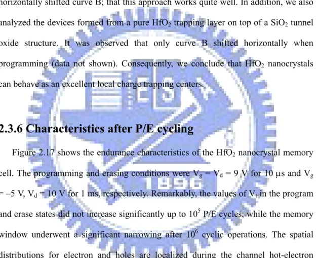
(16) Fig. 3.7 Vertical migration characteristics of HfO2 SONOS-type flash memories. Consistent with the former result, the vertical charge migration is exacerbated by increasing annealing temperature. Fig. 3.8 Read disturbance characteristics of HfO2 SONOS-type flash memories. No significant Vt shift for all samples even after 1000 seconds at 25°C. Fig. 3.9 Drain disturbance characteristics of HfO2 SONOS-type flash memories. After 1000 seconds at 25°C, only 0.4V drain disturb margin is observed for the 900ºC annealed devices. Fig. 3.10 Gate disturbance characteristics of HfO2 SONOS-type flash memories. Only 0.5V threshold voltage shift has been observed for the 900ºC annealed devices after Vg-Vt=7V and Vs=Vd=Vsub=0V, 1000 seconds stressing. Fig. 3.11 Plots of Icp vs Vgbl for the HfO2 memory cell after F–N programming to different Vt levels.. Chapter 4 Fig. 4.1 Schematic cross section and process flow of the high-κ dielectric poly-Si-TFT nonvolatile memories. Fig. 4.2 Cross-sectional HRTEM images of the gate stacks for the poly-Si-TFT memories with HfO2, Hf silicate and Zr silicate trapping layers. The inset show the diffraction patterns of them. Fig. 4.3 Demonstration of 2 bits/cell operation. E: erased; P: programmed; Bit1: drain side; Bit2: source side. Fig. 4.4 Programming and erasing speed characteristics of poly-Si TFT memories with HfO2, Hf silicate and Zr silicate trapping layers for different programming conditions. The programming time can be as short as 1ms if the window margin is set to 3V with Vg=Vd=12V. The erasing time is about 10 XIV.
(17) ms. Fig. 4.5 Retention characteristics of the fabricated poly-Si-TFT memories at T=25°C. The retention time can be up to 106 s for 20% charge loss at room temperature. Fig. 4.6 Endurance characteristics of the poly-Si-TFT memories. Despite the occurrence of significant memory window narrowing, a memory window of about 2V is sustained even after 105 P/E cycles. Fig. 4.7 Programming and erasing speed characteristics of poly-Si TFT memories with HfO2, Hf silicate and Zr silicate trapping layers for different programming conditions. The programming time can be as short as 1ms if the window margin is set to 3V with Vg=Vd=12V. The erasing time is about 10 ms. Fig. 4.8 Retention characteristics of the fabricated poly-Si-TFT memories with two different tunnel oxide thickness samples at T=25°C. Fig. 4.9 Retention characteristics of the fabricated poly-Si-TFT memories with two different tunnel oxide thickness samples at T=85°C. Fig. 4.10 Endurance characteristics of the poly-Si-TFT memories with two different tunnel oxide thickness samples. Fig. 4.11 The schematic illustration of disturb condition. Cell A is the programming cell. Cell B and Cell C are the drain disturbance and gate disturbance, respectively. Fig. 4.12 Drain disturbance characteristics of the Hf silicate TFT memory devicess with two different tunnel oxide thickness samples. After 1000 s at 25 °C, small 0.7V drain disturb margin was observed. Fig. 4.13 Gate disturbance characteristics of the Hf silicate TFT memory devices with two different tunnel oxide thickness samples. XV.
(18) Fig. 4.14 Read disturbance characteristics of the Hf silicate TFT memory devices with two different tunnel oxide thickness samples. No significant Vt shift occurred for Vd < 1, even after 1000 s at 25 °C.. Chapter 5 Fig. 5.1 HfO2 nanocrystal Flash memory cell structure. Fig. 5.2 (a) Planar-view HRTEM image of the 50nm HfO2 nanocrystals devices. (b) Planar-view HRTEM image of the HfO2 nanocrystals trapping layer. Fig. 5.3 Ids-Vgs curves of programmed memories with different programming conditions. The programming time is 10μs. A memory window of larger than 3V can be achieved with Vg= Vd=10V programming operation. Fig. 5.4 (a) Program characteristics of HfO2 nanocrystal memory devices with different programming conditions. (b). Erase characteristics of HfO2 nanocrystal memory devices with different erasing voltages. Fig. 5.5 Retention characteristics of HfO2 nanocrystal memory devices at T=25°C. Fig. 5.6 Endurance characteristics of HfO2 nanocrystal memory devices. Negligible degradation is found even after 105 P/E cycles. Fig. 5.7 Ids–Vgs Curves of the two-bit memory in a cell; forward read and reverse read for programmed bit1 and programmed bit2. Fig. 5.8 (a) Room-temperature hysteresis characteristics of the fabricated devices with various channel lengths. (b) The carrier mobiles with various channel lengths. Fig. 5.9 (a) Room-temperature hysteresis characteristics of the fabricated devices with various channel widths. (b) The carrier mobiles with various channel widths. Fig. 5.10 Read disturbance characteristics of the HfO2 nanocrystal memory devices. No significant Vt shift occurred for Vd < 4, even after 1000 s at 25 °C. XVI.
(19) Fig. 5.11 Drain current versus gate voltage characteristic. Fig. 5.12 Drain current versus gate voltage characteristic at low temperature (40°K) for different swept times. (a) delay=0 sec. (b) delay=0.1sec.. Chapter 6 Fig. 6.1 Schematic representation of the La2O3 SONOS-type Flash memory cell structure and localized charge storage. Fig. 6.2 Planar-view HRTEM image of the La2O3 SONOS-type memory. Fig. 6.3 Ids–Vgs Curves of the two-bit memory in a cell; forward read and reverse read for programmed bit1 and programmed bit2. Fig. 6.4 Program speed of the La2O3 SONOS-type memory Fig. 6.5 Erase speed of the La2O3 SONOS-type memory. Fig. 6.6 Retention of. the La2O3 SONOS-type memory for three temperature (T=25oC, 85oC,and 125oC). 22% charge loss occurred at 25 °C; and 40% charge loss occurred at 125 °C up to 108 sec.. Fig. 6.7 Endurance characteristics of the La2O3 SONOS-type memory after 10k P/E cycling. Fig. 6.8 Drain disturbance characteristics of the La2O3 SONOS-type memory. After 1000 s at 25 °C, only a 1V drain disturb margin was observed. Fig. 6.9 Gate disturbance characteristics of the La2O3 SONOS-type memory. A threshold voltage shift of only 1 V occurred after stressing at Vg = 10 V and Vs = Vd = Vsub = 0 V for 1000 s. Fig. 6.10 Read disturbance characteristics of the La2O3 SONOS-type memory devices. No significant Vt shift occurred for Vd < 4, even after 1000 s at 25 °C.. XVII.
(20) Table Lists Chapter 2 Table 2.1 Average elemental compositions in the HfSiOx silicate layers, as examined through EDS analysis of the as-deposited and 900°C-RTA-treated samples. Table 2.2 Comparison table of the different thickness samples of HfSiOx silicate layers after 900°C-RTA-treated. Table 2.3 Operation principles and bias conditions utilized during the operation of the HfO2 nanocrystal Flash memory cell. Table 2.4 Memory characteristics of the device fabricated in this study and the comparison with reported data for various SONOS-type memory cells.. Chapter 3 Table 3.1 Summary of the bias conditions for two-bit operation in the memory cell.. Chapter 4 Table 4.1 Operation principles and bias conditions utilized during the operation of the poly-Si TFT flash memory cell.. Chapter 6 Table 6.1 Operation principles and bias conditions utilized during the operation of the La2O3 SONOS-type memory cell.. XVIII.
(21) Chapter 1 Introduction 1.1 Background Recently,. complementary. metal-oxide-semiconductor. (CMOS). memory. technologies which driven by the more and more increasing demand for mobile capabilities, computer, and some electronic consumer products, have developed rapidly for the need in the people's livelihood. Memories can be divided into two main categories by whether the storage data can be affected by the power supply. One is volatile memory, and the other is non-volatile memory. Volatile memory will lose stored information once the power supply is switched off. On the other hand, nonvolatile memory does not lose its data when the system or device is turned off, and offer low power and high storage density solutions to generic needs of data storage. In 1967, D. Kahng and S. M. Sze invented the first floating-gate (FG) nonvolatile semiconductor memory at Bell Labs [1.1]. Recently, in order to improve the charge leakage and high power dissipation issues of volatile memory, the nonvolatile semiconductor memory devices play an important role in memory applications because of its low-voltage and low-power features for portable commercial devices. It stands out with its complementary metal oxide semiconductor (CMOS) compatibility and scalability to extremely high density. So far, the most widespread nonvolatile memory array is the so-called Flash memory, which has a byte-selectable programming operation combined with a sector erasing at the same time. In addition, as compared to the electrically programmable read-only memory (EPROM), and electrically erasable and programmable read-only memory (EEPROM), Flash memories have good flexibility of program/erase (P/E) operation, smaller area, and 1.
(22) low cost. The most well-known commercial Flash memory is Intel ETOX (EPROM Tunnel. Oxide). structure. (Figure. 1.1(a)). [1.2].. The. basic. device. is. a. Metal-Oxide-Semiconductor-Field-Effect-Transistor (MOSFET) with a modified gate stack structure that has a control gate (CG) and a floating gate (FG) embedded in a dielectric material such as silicon dioxide (SiO2). The memory storage element is the isolated floating gate disconnected from terminal voltages between the control gate and the channel. Figure 1.1(b) shows the band diagram of programming and erasing operations. The ETOX is “written” when we programmed the electrons into the floating gate by Channel-Hot-Electron (CHE) programming then the threshold voltage (VT) increases for the MOSFET. Otherwise, we erase the stored electrons and restoring VT to its original value by Fowler-Nordheim (FN) tunneling or band to band hot hole (BTBTHH) injection from FG to source [1.3]. The VT shift between the programmed and erased states is denoted by a quantity known as the “memory window.” Figure 1.2 shows a typical current versus gate voltage characteristic of an erased ETOX device and its VT shift when the device is programmed. The memory-state for the device can be determined by measuring the current in the MOSFET when a control gate bias is applied within the memory window. Nevertheless, the ETOX cell has several main drawbacks. Firstly, the Flash memory needs thick tunnel oxide (8~11 nm) to provide superior retention and endurance characteristics, but it also causes higher operation voltage, slow P/E speed, and poor scalability issues. Secondly, because the polysilicon floating-gate is conductive, the total charges stored in the floating gate will be easily leaked directly through the tunnel oxide when the tunnel oxide is damaged during P/E cycles (Figure 1.3(a)). Third, scaling the ETOX cell below the 0.1 μm feature size will be difficult; the main problems are related to high field stressing and the leaky scaled-down oxide barrier during the P/E cycle. To circumvent these limitations mentioned above, new 2.
(23) memory-cell structures with discrete traps as the charge storage elements (figure1.3(b)), e.g. MNOS (Metal / Nitride / Oxide / Silicon) [1.4], SONOS (Silicon / Oxide / Nitride / Oxide / Silicon) [1.5-1.6], and nanocrystal memory [1.7-1.8], have been demonstrated as the promising candidates in the Flash memory application. With the semiconductor technology continuously shrinks down to nano scale, the quality of ultra-thin tunnel oxide (<3nm) has been greatly improved. Therefore, nitride-related volume-distributed charge traps memories, such as metal nitride oxide silicon (MNOS) [1.4] and polysilicon oxide-nitride-oxide silicon (SONOS) [1.5-1.6], become more attractive in nonvolatile memory applications. However, for the MNOS devices, there have been shown an issue of charge leakage through the control gate. The top blocking oxide has to be introduced into the inter-layer between the control gate and the nitride layer, then the ONO (SiO2-Si3N4-SiO2) gate dielectric stack has been invent to improve the disadvantages. Therefore, the SONOS memory devices show greater retention and program/erase efficiency than MNOS counterparts. Figure 1.4 (a) illustrates the schematic of SONOS structure and the electron conduction paths. When the control gate is biased positively, electrons will tunnel from the channel through the SiO2 into the nitride layer. On the other hand, when the control gate is biased negatively, the trapped electrons are ejected into the channel by tunneling process. However, for the stored electrons in nitride layer, some electron move toward the gate or the channel even though they are blocked by the top oxide or the tunnel oxide because the shallow trap level in the nitride layer [1.9]. The charge transport mechanisms involve FN-tunneling, direct tunneling and Frenkel-Poole emissions (Figure 1.4 (b)). (A Frenkel-Poole emission is the electric field-assisted and thermal excitation of trapped electrons in defects to the conduction band.) For the operation, SONOS devices can be written with less then 10 V in one micron-second. So far, SONOS memories have the huge market in the Flash memory application. 3.
(24) SONOS-type (poly-Si-oxide-nitride-oxide-silicon) Flash memories have recently attracted much attention for the application in the next-generation nonvolatile memories [1.10]. High-κ dielectric materials would be able to maintain an equivalent potential difference between the floating gate and the device body for a greater thickness compared to SiO2. The leakage through the dielectric would be minimized and the scaling limits would be extended. Moreover, to achieve a memory window that can differentiate between stable program and erased states, using high-κ dielectric trapping layer can has sufficiently high node density for the memory. Using the high-k trapping layer exhibits many advantages, e. g., easy to fabricate, high program/erase speed, low programming voltage and power consumption, better potential for scalability below the 70-nm node, according to the International Technology Roadmap for Semiconductors (ITRS) [1.11]. Hafnium oxide (HfO2) is considered to be a promising candidate for the charge trapping layer for the SONOS-type Flash memory instead of Si3N4 film [1.12]. The high-κ dielectric film, HfO2, is expected to have better charge trapping characteristics than the conventional Si3N4 films for sufficient density of trap states and deep trap energy level to achieve longer retention time [1.13-1.14]. This feature makes HfO2 be more helpful in scaling the tunnel oxide for enhancing the performance and more suitable for the development of the SONOS-type memory with multi-bit operation [1.15-1.16]. Unfortunately, many concerns still remain for this type of memories. For conventional SONOS memory, erase saturation and vertical stored charge migration [1.17-1.18] are two major drawbacks (Figure 1.5(a)(b)). So, nanocrystal memories have been invented because their very local charge storage. Unlike volume-distributed charge traps memories, nanocrystals can be uniformly deposited as a two-dimensional (2-D) distribution on a thin tunnel oxide as illustrated in Figure 1.6(a). The nanocrystal can store the charge locally due to the well isolation 4.
(25) of nanocrystals from each other and effectively prevents formation of good conductive paths between the adjacent nodes (figure 1.6(b)). Generally, nanocrystals are small clusters of silicon atoms with size of 5 to 10 nm in diameter. By limiting nanocrystal deposition to just one layer and adjusting the thickness of top blocking oxide, charge leakages to the control gate from the storage nodes can be effectively prevented (figure 1.6(b)). In recent years, Si and Ge nanocrystals have been studied extensively. IBM researchers, Tiwari et al., first proposed a Si nanocrystal nonvolatile memory with a granular floating gate in 1995 [1.7], and a higher P/E speed than Flash memory has been reported. In 1998, King et al. has published the Ge dot nanocrystal memory [1.8]. So far, Si and Ge nanocrystals can be fabricated by various techniques, including chemical vapor deposition [1.7][1.19], low energy ion implantation [1.20], annealing of silicon rich oxide [1.21], thermal oxidation of SiGe [1.22], and aerosol nanocrystal formation [1.23]. Moreover, Lee et al. has reported a new method to improve the memory characteristics of the Si nanocrystal memory devices by replacing the traditional SiO2 with HfO2 high-κ dielectrics [1.24]. In 2002, Liu et al. has proposed the self-assembled nanocrystal formation process and the design principles of the metal nanocrystal memories with Au, Ag, and Pt materials [1.25-1.26]. The nanocrystals are formed self-assembly by depositing an ultra-thin metal layer on the gate oxide and then annealing by rapid thermal annealing (RTA) system. In addition, the higher density of states, stronger coupling with the channel, better size scalability, and the design freedom of engineering the work function to optimize device characteristics are the advantages of metal nanocsrystals over their semiconductor counterparts. Flash memories (SONOS memories, SONOS-like memories, and nanocrystal memory) have widest applications in nonvolatile memories due to their enhanced flexibility and higher effective speed and density. They provide single cell electrical 5.
(26) program and fast simultaneous block electrical erase. For combined with a fast in-system erase capability, these low-power and robust Flash systems are ideal for a myriad of portable applications such as cellular phones, pagers, digital cameras, digital voice recorders, personal data assistants to compact smart cards. They even may eventually replace the ubiquitous magnetic memory media and RAMs (Random Access Memories) in many compact electronic applications. As consumer electronics evolve towards ever-higher performance and multi-functionality, the System-On-Chip (SOC) concept for ultra-large scale integration (ULSI) of microelectronic devices is gaining momentum. This circuit-level integration concept broadly encompasses approaches where functionally distinct modules (e.g. digital logic, memory, analog components and signal processing) are intimately integrated on a single chip to increase system speed and capability. Since many of the device modules have very different material, thermal, and contamination process requirements, the search for compatible process recipes for these devices has major challenges.. 1.2 Motivation In this thesis, we have designed a high performance nonvolatile memory with HfO2 nanocrystal charge-trapping layer and high-κ charge-trapping layer such as HfO2 and La2O3. These high-κ layers replace the silicon nitride layer in the SONOS structure. Different program/erase methods are also proposed for low power applications. These nonvolatile memory structures will have superior characteristics in terms of considerably large memory window, high speed program/erase, long retention time, and excellent endurance. High-κ dielectric materials, such as HfO2, ZrO2, La2O5, and Pr2O3, will be used to fabricate the charge-trapping layer. These materials provide high trapping state. 6.
(27) densities and deep trapping levels, therefore they can enhance the retention of nonvolatile memories. The charge-trapping efficiency can be improved, and larger operation window can be achieved. The application of high-k materials can further reduce the operation voltage and potentially can help memory device scaling. A novel nanocrystal charge-trapping layer can be fabricated by annealing high-κ silicate materials, such as HfSixOy. After applying a rapid thermal anneal to the silicates, phase-separation happens. HfO2 nanocrystals are formed and surrounded by SiO2. With such a nanocrystal structure as the charge-trapping layer, the retention of nonvolatile memories can be further improved. The stored charges will be trapped in/around the nanocrystals and isolated by silicon dioxides. Less opportunity of charge loss is expected. For the memory device operation, we use channel hot-electron injection for the programming and band-to-band hot-hole injection for the erase. Staying in oxide trapping states or high-k nanocrystals, the stored charges are separated at different trapping sites. A local defect of tunnel oxide won’t cause a severe charge loss. Thus we can achieve 2 bits storage in one memory device by reversing source and drain. Using band-to-band hot-hole injection can alleviate the drawback of over-erase, which is a problem when FN-tunneling is utilized. We will study the influences of different program/erase operations on the reliability issues of nonvolatile memories. Moreover, we also used three kinds of high-κ dielectrics, including HfO2, Hf-silicate and Zr-silicate for the trapping layer of the poly-Si TFT memory. Polycrystalline silicon thin-film transistors (Poly-Si-TFT) have been widely used to integrate driver circuits for the application of AMLCD’s [1.27]. The feasibility of integrating an entire system on top of the panel (SOP) is being actively pursued [1.28]. By employing low thermal cycle (600°C, 24hrs) for post high-κ deposition annealing and S/D activation, the proposed nonvolatile memory fabrication is fully compatible 7.
(28) with the current mass-production TFT processing. This makes the realization of producing the embedded nonvolatile memories on the panel becomes feasible. The goal of this thesis is to find an optimized nonvolatile Flash memory in the application of congenital CMOS process and poly-Si-TFT process. By evaluating different materials and fabrication processes, we intend to find a replacement for silicon nitride as the charge-trapping layer. Therefore we can benefit from the low power operation and still maintain good reliabilities of nonvolatile memory devices. The high-k nanocrystals also has potential applications for CMOS and quantum devices.. 1.3 Thesis Organization We will propose a novel, simple, reproducible, and reliable technique for the design of high-density HfO2 nanocrystal Flash memories through the spinodal decomposition of hafnium silicate in chapter 2. Then, in the chapter 3, we have investigated the effect of post-deposition annealing temperature on the performance of the resultant HfO2 SONOS-type Flash memories. In the chapter 4, we have studied three kinds of high-k dielectrics, including HfO2, Hf-silicate and Zr-silicate for the trapping layer of the low temperature poly-Si-TFT memory devices with two different thickness tunnel oxides. In chapter 5, 50nm nano scaled tri-gate HfO2 nanocrystals Flash memories have been fabricated on SOI. In the chapter 6, we have investigated the La2O3 trapping layers for the SONOS-type Flash memories. Conclusions follow in chapter 7.. 8.
(29) (a). (b). Fig. 1.1 (a)Schematic of a basic ETOX Flash memory device. (b) Electron flow (red arrows) during programming by CHE injection. Electron flow (green arrows) or hole flow (orange arrows) during erasing by FN tunneling or BTBTHH injection to the source. [1.2] 9.
(30) Fig. 1.2 Current-voltage characteristic of a memory device in the erased and programmed state, showing the VT shift and the memory window.. 10.
(31) (a). (b). Fig. 1.3 (a) Charges in the dielectric stored in isolated storage nodes. (b) A schematic of a continuous FG structure with all the charges drained by an isolated defect in the dielectric. 11.
(32) (a). (b) Fig. 1.4 (a) Basic SONOS memory device structure. Red arrows show paths of electron transport during memory operation. The electrons hop between trap. (b) Energy diagram illustrating the physical process of a typical SONOS program operation sites (blue dots) within the Si3N4 layer. 12.
(33) (a). (b). Fig. 1.5 (a) Vertical migration of the stored charge in the Si3N4 trapping layer in SONOS memory device structure. (b) Lateral migration of the stored charge in the HfO2 trapping layer in SONOS memory device structure.. 13.
(34) (a). (b). Fig. 1.6 (a) An illustration of a nanocrystal Memory. (b) The nanocrystal can store the charge locally due to the well isolation of nanocrystals from each other and effectively prevents formation of good conductive paths between the adjacent nodes. 14.
(35) Chapter 2 Characteristics of HfO2 Nanocrystal Nonvolatile Flash Memory 2.1 Introduction SONOS-type (poly-Si-oxide-nitride-oxide-silicon) structure memories, which include nitride and nanocrystal memories, have recently attracted much attention for their application in the next-generation nonvolatile memories [2.1–2.10]. They exhibit many advantages, e. g., easy to fabricate, high program/erase speed, low programming voltage and power consumption, better potential for scalability below the 70-nm node, according to the International Technology Roadmap for Semiconductors (ITRS) [2.11]. Unfortunately, many concerns still remain for this type of memories. For conventional SONOS memory, erase saturation and vertical stored charge migration [2.7-2.8] are two major drawbacks. While, for nanocrystal memories, the most challenging tasks are how to maintain acceptable charge capability of the discrete storage nodes and fabricate nanocrystals with constant size, high density, and uniform distributions [2.9]. In recent years, various ONO processing technology [2.10] and alternative trapping layer material [2.12] have been investigated to improve the cell data retention. For example, the use of an Al2O3 trapping layer and HfAlO3 to replace Si3N4 have been considered since their material bandgaps and high trap densities provide superior program/erase speed and data retention [2.12-2.13]. Moreover, various kinds of nanocrystals, such as silicon (Si), germanium (Ge), and metal nanocrystals, may be used to provide charge storage for nonvolatile memories [2.1-2.6]. In this chapter, we propose a novel technique which is fully compatible with the. 15.
(36) current CMOS technologies, in forming very localized HfO2 nanocrystals for application in high-density two-bit nonvolatile Flash memory. This approach utilizes spinodal decomposition of hafnium silicate after RTA treatment at a sufficiently high temperature [2.14-2.15]. Using this technique, we can readily isolate the HfO2 nanocrystals from each other within a SiO2-rich matrix. With a large band gap offset between HfO2 and SiO2, memory cell using HfO2 nanocrystal may exhibit superior characteristics, such as a larger memory window, high program/erase speeds, long retention time, excellent endurance [2.16-2.17], and strong immunity against disturbance. In addition, by comparing to those published ones using Si, Ge, and metal nanocrystals [2.1-2.6], our HfO2 nanocrystal memory possesses many advantages, such as larger memory window and better data retention. Moreover, high temperature process for the S/D activation is no longer detrimental because this step can help further stabilize the HfO2 nanocrystal; while it will oxidize the other nanocrystals and lead to a decrease in memory window. The process is very simple, reproducible, and reliable with less metal contamination concern.. 2.2 Experimental An example of the fabrication process of the HfO2 nanocrystal memory devices is demonstrated by a LOCOS isolation process on a p-type, 5–10 Ω cm, (100) 150-mm silicon substrate (Fig. 2.1). First, a 2nm tunnel oxide was thermally grown at 1000 °C in a vertical furnace system. Next, a 12nm amorphous HfSiOx silicate layer was deposited by co-sputtering with pure silicon (99.9999% pure) and pure hafnium (99.9% pure) targets in an oxygen gas ambient. The co-sputtering process was performed with 7.6 ¯ 10–3 Torr at room temperature and with precursors of O2 (3 sccm) and Ar (24 sccm); in which both dc sputter powers were set at 150 W. The. 16.
(37) samples were then subjected to RTA treatment in an O2 ambient at 900 °C for 1 min to convert the HfSiOx silicate film into the separated HfO2 and SiO2 phases. Their compositions were identified using both energy-dispersive spectroscopy (EDS) and X-ray photoelectron spectroscopy (XPS). A 8nm blocking oxide was then deposited through high-density-plasma chemical vapor deposition (HDPCVD), followed by a N2 densification process at 900 °C for 1 min. Subsequently, poly-Si deposition, gate patterning, source/drain (S/D) implanting, and the remaining standard CMOS procedures were completed to fabricate the HfO2 nanocrystal memory devices.. 2.3 Results and Discussion 2.3.1 Material Analysis of HfO2 Nanocrystals Figure 2.2 shows planar-view high-resolution transmission microscopy (HRTEM) image of the HfO2 nanocrystals. The average nanocrystal size was 5–8 nm; the density was as high as 0.9–1.9 ¯ 1012 cm–2. Clearly, the nanocrystals were well separated in two dimensions within the SiO2; in which the average distance is >5 nm. This isolation of the nanocrystals prevents the formation of effective conductive paths between adjacent nodes. The mechanism responsible for the formation of HfO2 nanocrystal is through the phase separation of hafnium silicate into a crystallized structure [2.14]. For the Hf-silicate layer, the compositions within metastable extensions of the spinodal are unstable and HfO2 nanocrystal will be formed and wrapped up by SiO2 after cooling down from RTA processing. In addition, it is clear from the diffraction patterns that the as-deposited film was amorphous and that the sample subjected to RTA was polycrystalline. The HfO2 nanocrystals have monoclinic crystalline structures. Table 2.1 lists the original average concentrations of the individual elements in the as-deposited amorphous HfSiOx silicate layer, as 17.
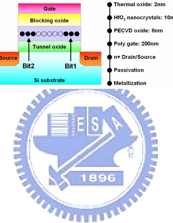
(38) determined through EDS analysis at a spatial resolution less than 2.0 nm. We observe that the as-deposited HfSiOx layer comprised ca. 40 mol% HfO2 and 60 mol% SiO2; the average elemental concentrations of Hf, Si, and O were 12.61, 18.99, and 68.40%, respectively. At this elemental composition, we can readily reproduce high-density HfO2 nanocrystal dots embodied within a SiO2-rich matrix after RTA in an O2 ambient. Moreover, we also deposited 2nm and 6nm amorphous HfSiOx silicate layer by the same co-sputtering conditions. The samples were also subjected to RTA treatment in an O2 ambient at 900 °C for 1 min to convert the HfSiOx silicate film into the separated HfO2 and SiO2 phases. Figure 2.3 (a) and 2.3 (b) show the planar-view high-resolution transmission microscopy (HRTEM) image of the HfO2 nanocrystals for the different thickness samples. With the thickness increases, the better HfO2 nanocrystals form, the HfO2 nanocrystal size increases, but the nanocrystal destiny decreases. Table 2.2 shows the comparison table of the different thickness samples of HfSiOx silicate layers after 900°C-RTA-treated. We have also performed X-ray photoelectron spectroscopy (XPS) measurements using an Al Kα X-ray source (1486.6 eV photons) to determine the bonding environments of the Hf and Si atoms. Fig. 2.4(a) shows the Hf 4f photoemission peaks of the as-deposited Hf-silicate film before and after its PDA at 900 °C under O2. In the as-deposited film we observe well-defined 4f5/2 and 4f7/2 feature peaks that correspond to Hf–O–Si bonding. We confirmed that HfO2 nanocrystals formed after RTA through the observed shifts of these peaks to lower binding energies (4f5/2: ca. 18.9 eV; 4f7/2: ca. 17.4 eV) [2.18-2.19]. Fig. 2.4(b) shows Si 2p XPS spectra of the as-deposited Hf-silicate film before and after RTA. Again, the Si–O bonds in SiO2 network (104 eV) are prominent; their peak intensity increased after PDA. These results provide definite evidence for phase separation occurring in the PDA-treated 18.
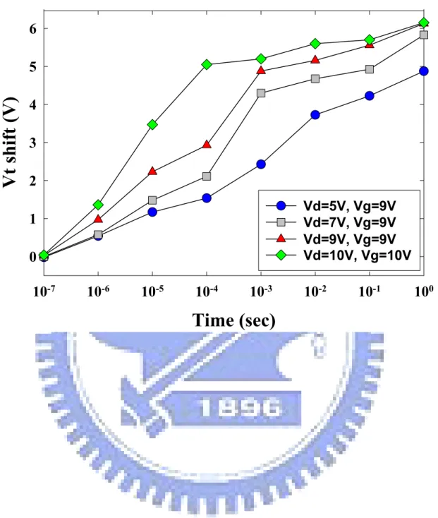
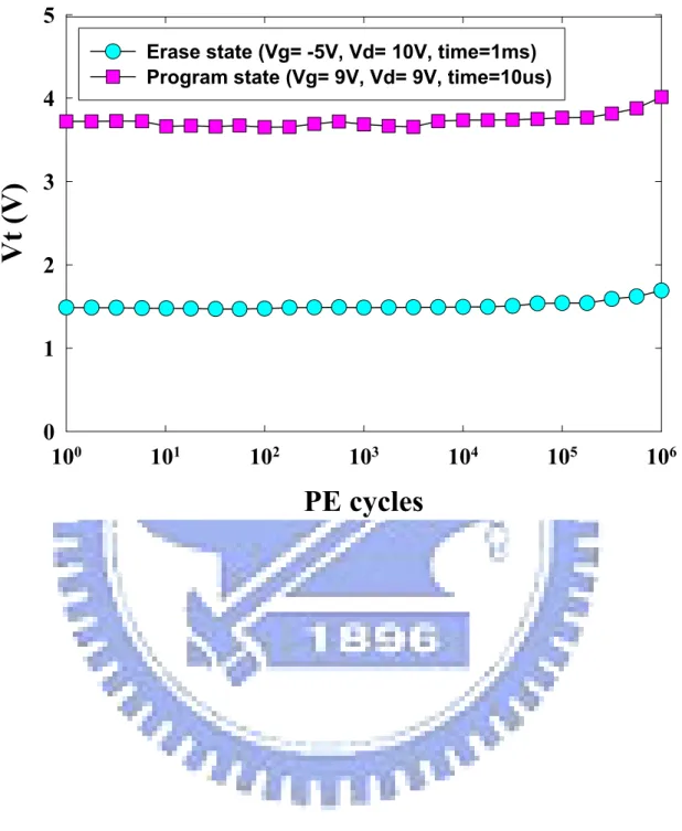
(39) Hf-silicate film.. 2.3.2 Characteristics of Fresh Devices and 2-bit operation Figure 2.5 shows the Ids-Vgs curves of the HfO2 nanocrystal memory devices with programming time of 10μs for different programming conditions. Channel hot-electron injection and band-to-band hot-hole injection were employed for programming and erasing, respectively. All cells described in this chapter have dimensions of L/W = 1/2 μm. A relatively large memory window of about 3V can be achieved at the Vg=Vd=10V program operation. Program characteristics as a function of pulse width for different operation conditions are shown in Fig. 2.6(a). Both source and substrate terminals were biased at 0V. The “Vt shift” is defined as the threshold voltage change of a device between the written and the erased states. With Vd=Vg=9V, relatively high speed (10μs) programming performance can be achieved with a memory window of about 2.2V. Meanwhile, Fig. 2.6(b) displays the erase characteristics as a function of various operation voltages. Again, excellent erase speed of around 0.1 ms can be obtained. More important, there is only a very small amount of over-erase observed. The reason is owing to the fact that the vertical electric field decreases with decreasing amount of trapped electrons in the nanocrystals during erasing and the hole injection into the nanocrystals will reduce significantly due to the higher hole tunneling barrier presented in HfO2/SiO2 stack after all programmed charges are removed [2.20]. The retention characteristics of the HfO2 nanocrystal memory devices at both room temperature (T=25°C) and higher temperature (T=125°C) are illustrated in Fig. 2.7. The retention time can be up to 108 seconds for 10% charge loss at room temperature. Only slight charge loss has been seen even at the temperature up to. 19.
(40) 125°C. We ascribe these results to the combining effects of the tight embrace of HfO2 nanocrystals by SiO2-rich matrix and the sufficiently deep trap energy level [2.20]. Therefore, albeit with a tunnel oxide down to 2nm in thickness, no significant lateral and vertical charge migrations occurred. As a result, superior retention characteristic of the charge storage can be procured. The endurance characteristics after 106 P/E cycles are also shown in Fig. 2.8. The programming and erasing conditions are Vg=Vd=9V for 10μs and Vg=-5V, Vd=10V for 1ms, respectively. No detectable memory window narrowing has been displayed. Moreover, the individual threshold voltage shifts in program and erase states only become visible after 105 cycles. This trend indicates that the amount of operation-induced trapped electrons is very tiny. Certainly, this is intimately related to the use of ultra-thin tunnel oxide and very minute amount of residual charges in the HfO2 nanocrystals after cycling.. Fig. 2.9. demonstrates the feasibility of performing two-bit operation with our HfO2 nanocrystal memories through a reverse read scheme in a single cell. From the Ids–Vgs curves, it is clear that we could employ forward and reverse reads to detect the information stored in the programmed bit1 and bit2, respectively. The read operation was achieved using a reverse read scheme. Table 2.3 summarizes the bias conditions for two-bit operation.. 2.3.3 Migration of storage charges One of the major advantages that HfO2 nanocrystal Flash memory has over floating gate Flash EEPROM is its better data retention, which is attributed to its excellent capability of locally trapping charges with no significant lateral or vertical migration. We can measure the degrees of migration from the cells after the cycling. One method for characterizing the lateral extent of the trapped electrons is to monitor. 20.
(41) the variation of the threshold voltage (Vt) for a programmed memory cell in the presence of a changing drain current (Vd) [2.19]. Fig. 2.10 shows a plot of the measured Vt versus Vd as a function of the measuring temperature in a programmed cell after 10k P/E cycling. Here, Vt is defined as the applied gate voltage at which the drain current is 1 μA. Since channel hot-electron injection is used for the cell programming, the trapped electrons in the HfO2 nanocrystal trapping layer are more likely to be located near the n+ drain junction. These trapped electrons will raise the potential barrier near the drain side and increase the value of Vt. The degree of the Vt shift is believed to be proportional to the trapped electron density if the drain terminal is maintained at a relatively low potential (e.g., Vd = 0.1 V). When a sufficiently high drain bias (e.g., Vd = 1.5 V) is applied, however, the drain depletion region will be extended toward the channel and, consequently, block the influence from the trapped electrons for the measured Id–Vg characteristics [2.21]. Therefore, this proposed technique can detect the lateral profile of the trapped electrons. To enhance the storage charge movement in the HfO2 nanocrystal trapping layer, the programmed samples were subjected to high-temperature baking at 80 and 125 °C for 2000 s, respectively. Remarkably, the Vt–Vd curves for the cycled device and the baked devices exhibit very little difference, suggesting that lateral migration of the storage charges in the HfO2 nanocrystal trapping layer is rather insignificant. It was attributed to the effective isolation of each nanocrystal within the SiO2 matrix. Next, we investigated the influence of the vertical field on charge retention, i.e., vertical migration. Fig. 2.11 shows the Vt variation over time for various stress conditions for the 10k P/E cycled cells. Visible charge loss was observed when the applied gate voltage and temperature were raised up to -5V and 125°C. We thought even though the trap energy level in the nanocrystal is quite deep, the generated defects and interface traps of the 2nm tunnel oxide after 10k P/E cycled stress will help stored 21.
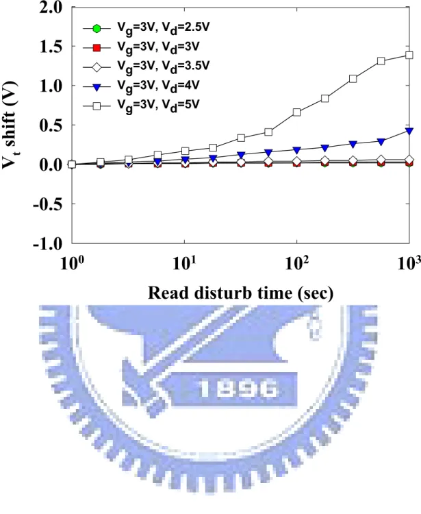
(42) charges escape via trap-assisted tunneling. Therefore, vertical charge migration is more observable than lateral charge migration in our memory cell. We also calculated the activation energy for the traps of the HfO2 nanocrystals in the new cells (Fig. 2.12). Activation energy tracing is used widely to characterize the Arrhenius relation extracted from the temperature dependence of charge loss from nonvolatile memory as a function of time. For a given charge loss threshold criterion (in our case, 20% is used), the failure rates obtained at high temperature (125–200 °C) can then be extrapolated to the nominal operating conditions. The model is based on a classical temperature-activated Arrhenius law, expressed in the form tR = t0 × eEa/kT, where t0 is the retention time corresponding to an infinite temperature, Ea is the activation energy, T is the temperature, and k is the Boltzmann constant [2.22]. The activation energy, determined from the slopes of five samples, lies in the range 2.1–3.3 eV, Obviously, it is higher than those values previously reported for conventional SONOS memories [2.23-2.25].. 2.3.4 Disturbance Figure 2.13 demonstrates the read disturbance induced erase-state threshold voltage instability in a localized HfO2 nanocrystal trapping storage Flash memory cell under several operation conditions. For two-bit operation, the applied bitline voltage in a reverse-read scheme must be sufficiently large (>1.5 V) to be able to “read through” the trapped charge in the neighboring bit. The read-disturb effect is the result of two factors: the word-line and the bit-line. The word-line voltage during read may enhance room temperature (RT) drift in the neighboring bit [2.26]. On the other hand, a relatively large read bit-line voltage may cause unwanted channel hot-electron injection and, subsequently, result in a significant threshold voltage shift of the 22.
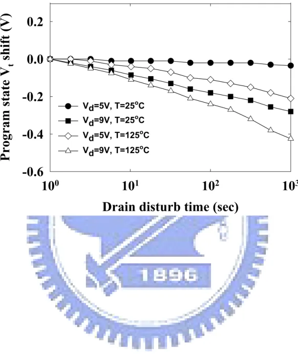
(43) neighboring bit. In our measurements, the gate and drain biases were applied and the source was grounded. The results demonstrate clearly that almost no read disturbance occurred in our HfO2 nanocrystal Flash memory under low-voltage reading (Vg = 3 V; Vd = 2.5 V). For a larger memory window, we found that only a small read disturbance (ca. 0.3 V) can be observed after operation at Vd = 4 V after 1000 s at 25 °C. Figure 2.14 shows the programming drain disturbance of our HfO2 nanocrystal Flash memory. Two different drain voltages (Vd = 5 and 9 V) were applied in the programming drain disturbance measurements at two different temperatures (T = 25 and 125 °C). We observed that a sufficient programming drain disturb margin exists (ΔVt < 0.4 V), even after programming at a value of Vd of 9V under high temperature (T = 125 °C) and after stressing for 1000 s. Fig. 2.15 shows the gate disturbance characteristics in the erasing state. Gate disturbance may occur during programming for the cells sharing a common word-line while one of the cells is being programmed. We observed a threshold voltage shift of only 0.16 V, i.e., negligible disturbance, under the following conditions: Vg = 9 V; Vs = Vd = Vsub = 0 V; stressed for 1000 s. It in interested to know why this memory can exhibit such excellent gate disturb characteristics with such a thin tunnel oxide; a non-negligible current will be present in the tunnel oxide when a voltage of 9 V is applied to the gate electrode. Using a serial capacitor voltage divider model, we estimated that the voltage drop at the tunnel oxide would be 0.98 V if the trapping layer is assumed to be a HfO2 film, rather than nanocrystal. Even though a 0.98V drop will cause a significant leakage current through an individual 2nm oxide layer, the data retention in the memory cell is related not only to the direct tunneling leakage current induced by such a voltage but also to the total tunneling situation in the whole gate stack; i.e., the effect that the potential barrier presented by the high-k material has on the tunneling current must be taken 23.
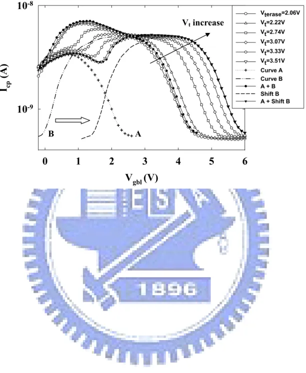
(44) into account. In other words, it is incorrect to state that a large direct tunneling current will definitely exist in the interfacial layer and, in turn, that it will induce significant disturbance during programming.. 2.3.5 Charge pumping characteristics The charge pumping (CP) measurement was used to investigate the characteristics of our HfO2 nanocrystal Flash memory. We used a trapezoidal gate pulse having a fixed pulse amplitude with a varying Vgbl. The substrate current (the so-called “charge pumping current,” Icp) as a function of Vgbl was measured. The gate pulse have a frequency of 1 MHz and a 50% duty cycle; the rising and falling times were both 2 ns. Fig. 2.16 shows plots of the program state charge pumping current Icp versus Vgbl for our HfO2 nanocrystal memory cell. Fowler–Nordheim tunneling was used to program the cell with Vt levels from 2.06 to 3.51 V. The open symbols represent the measured data. The program state Icp curve shifted increasingly toward the right upon increasing the value of Vt as a result of an increase in the amount of injected charge in the HfO2 nanocrystal trapping layer. Interestingly, a hump appeared in the left-hand edge of the curve in compliance with this shift. We decompose the resultant Icp curve mathematically into two individual curves, A and B, in a fresh memory cell. We speculate that these two Icp curves arise from interlacing of the SiO2 matrix and HfO2 nanocrystals within the trapping layer. In other words, the memory is composed of two kinds of devices that have different gate dielectric configurations. The extracted threshold voltage in curve A is larger than that in curve B, even for a fresh memory; because the value of EOT of the gate stack in the region containing SiO2 matrix is larger than that in the part containing the HfO2 nanocrystals. We believe that curve A is related to the SiO2 matrix and curve B corresponds to the HfO2. 24.
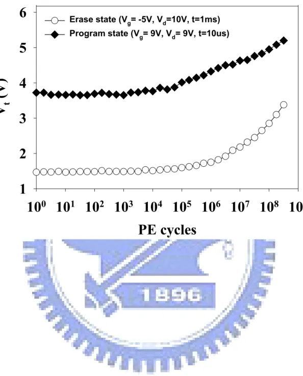
(45) nanocrystals. With programming, it is clear that the Icp curve arising from the region containing the SiO2 matrix undergoes almost no shift and the resultant distortion appearing in the measured Icp curve is caused mainly by the charging of the HfO2 nanocrystal. This result implies that the programming charge was stored almost entirely within or around the HfO2 nanocrystal, rather than in the SiO2 matrix. To confirm this hypothesis, we traced the measured curve by adding curve A to a horizontally shifted curve B; that this approach works quite well. In addition, we also analyzed the devices formed from a pure HfO2 trapping layer on top of a SiO2 tunnel oxide structure. It was observed that only curve B shifted horizontally when programming (data not shown). Consequently, we conclude that HfO2 nanocrystals can behave as an excellent local charge trapping centers.. 2.3.6 Characteristics after P/E cycling Figure 2.17 shows the endurance characteristics of the HfO2 nanocrystal memory cell. The programming and erasing conditions were Vg = Vd = 9 V for 10 μs and Vg = –5 V, Vd = 10 V for 1 ms, respectively. Remarkably, the values of Vt in the program and erase states did not increase significantly up to 105 P/E cycles, while the memory window underwent a significant narrowing after 106 cyclic operations. The spatial distributions for electron and holes are localized during the channel hot-electron injection and band-to-band hot-hole injection for the programming and erasing, respectively, of our HfO2 nanocrystal memory. If the electron distribution does not completely match that for the hole, then each P/E cycle will leave a few electrons in the trapping layer [2.27]. This so-called “hard-to-erase” phenomenon cannot be eliminated readily when using band-to-band hot-hole erasing. Obviously, this is not an issue for our memory because the enhanced local electric field across the thin tunnel. 25.
(46) oxide in the region just beneath the nanocrystals can help in the injection of holes. Fig. 2.18 illustrates the retention characteristics of the HfO2 nanocrystal memory devices for a 10k P/E stressed HfO2 nanocrystal memory cell both at room temperature (T = 25 °C) and above (T = 125 °C). Relative to the fresh device, the device operated at room temperature retained its good retention time (up to 105 s) for 10% charge loss [16]. We ascribe this result to the combined effects of the tight embrace of the HfO2 nanocrystals by the SiO2-rich matrix and the sufficiently deep trap energy level of our memories (extracted activation energy: 2.1–3.3 eV). Therefore, despite the tunnel oxide having a thickness as low as 2 nm, no significant lateral or vertical charge migration occurred; as a result, the device displays superior retention characteristics for charge storage. At the temperature at 125 °C, we observed a more significant charge loss during the program state. This strong temperature-dependence was predictable from the large activation energy, but the detailed mechanism remains under further investigation. Table 2.4 presents a comparison of our results with those of recent investigations into new devices [2.2, 2.5, 2.8]. Our system shows a number of salient features. First, our HfO2 nanocrystal memories exhibit larger memory windows than do the other systems because of the large trap density of the high-k dielectric materials. Second, with respect to the P/E speed, we obtained a high speed of operation because we used channel hot-electron programming and band-to-band hot-hole erasing. Finally, we observed good retention with no vertical or lateral migration as a result of the HfO2 nanocrystals being isolated effectively within the SiO2 matrix.. 2.3.7 Characteristics of different tunnel oxide thickness Figure 2.19 and 2.20 show the programming and erasing characteristics,. 26.
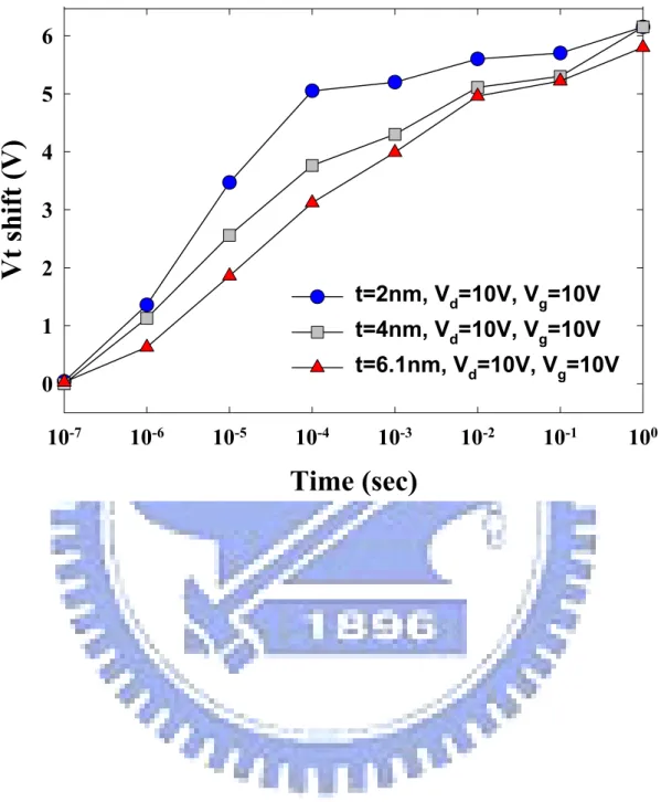
(47) respectively, of the fabricated HfO2 nanocrystal memory with three different tunnel oxide thicknesses, 2nm, 4nm and 6.1nm, respectively. We programmed with the bias condition at Vg = 10V and Vd = 10V and erased with the bias condition at Vg = 10V and Vd = -5V. We observed that the memory with thinner tunnel oxide exhibited slightly improved programming speed when they were operated with the short pulse widths and better erase performance. Fig. 2.21 illustrates the retention characteristic of the fresh HfO2 nanocrystal memory with three different tunnel oxide thicknesses at different testing temperatures. For all cases, the retention times can be extrapolated up to more than 108 seconds for 15% charge loss at room temperature. Such good retention performance can be ascribed to the sufficiently deep trap energy levels in hafnium silicate. We also calculate the activation energy of the traps in the HfO2 nanocrystals for the fresh device with different tunnel thickness in the figure 2.22. For a given charge–loss threshold criterion (in our case, 20%), the obtained failure rate can then be extrapolated to the nominal operating condition. The activation energy, determined from the slopes of five samples, lies in the range 2.1–3.3 eV, 2.46-3.11eV, and 2.95-3.26eV for the 2nm, 4nm, and 6.1nm samples, respectively. Therefore, we thought that the sample with thick tunnel oxide can be employed for achieving better charge keeping capability. For the thicker sample, the activation energy lies in the narrow range because more uniform tunnel oxide of 6.1nm. The thinner tunnel oxide of 2nm may have more leakage path for the charge during the temperature stress. Obviously, these values also lie in the higher ranges of those scattered values previously reported for the conventional SONOS memories. The endurance performances of the HfO2 nanocrystal memory with different tunnel oxide thicknesses are shown in Fig. 2.23. Despite the occurrence of significant memory window narrowing, a memory window of about 2V sustained even after 105 P/E cycles. The origin of the narrowing over cycling might be due to two factors. First is the mismatch 27.
數據
+7
相關文件
In this chapter we develop the Lanczos method, a technique that is applicable to large sparse, symmetric eigenproblems.. The method involves tridiagonalizing the given
In this paper, we have shown that how to construct complementarity functions for the circular cone complementarity problem, and have proposed four classes of merit func- tions for
In this paper, we develop a novel volumetric stretch energy minimization algorithm for volume-preserving parameterizations of simply connected 3-manifolds with a single boundary
In this study, we compute the band structures for three types of photonic structures. The first one is a modified simple cubic lattice consisting of dielectric spheres on the
We have also discussed the quadratic Jacobi–Davidson method combined with a nonequivalence deflation technique for slightly damped gyroscopic systems based on a computation of
雙極性接面電晶體(bipolar junction transistor, BJT) 場效電晶體(field effect transistor, FET).
In this paper, a novel subspace projection technique, called Basis-emphasized Non-negative Matrix Factorization with Wavelet Transform (wBNMF), is proposed to represent
In this chapter, a dynamic voltage communication scheduling technique (DVC) is proposed to provide efficient schedules and better power consumption for GEN_BLOCK
