RFIT2005-IEEE InternationalWorkshoponRadio-Frequency IntegrationTechnology,Nov30-Dec02, 2005, Singapore
A
Ku-band
CMOS
Low-Noise
Amplifier
PIO
Kuo-Liang Deng, Ming-Da Tsai,
Chin-ShenLin,
Kun-YouLin,
HueiWang,
S. H.
Wang*, W. Y.
Lien* and JohnG. J. Chern*
Departmentof ElectricalEngineeringandGraduateInstituteofCommunicationEngineering, NationalTaiwanUniversity, Taipei, Taiwan, R.O.C.
*Taiwan SemiconductorManufacturing Co., Hsinchu, Taiwan, 300, R.O.C. Email:
hueiwangAiew.ee.ntu.edu.tw
Abstract-A Ku-band monolithic low-noise amplifier is presented inthis paper. This LNA fabricated in commercial 0.18-pm CMOS technology is a two-stage common-source
design instead of cascode configuration for lower noise performance. This CMOS LNA demonstrates againof better than 10 dB andaNFof better than 3.2 dB from 14to15GHz. The measuredoutput
PIdB
is about5.2 dBm andinputIP3 is 1.6 dBm. The chip sizeincludingalltestingpads is 0.88x 0.77 mm2.Index Terms-Ku band, CMOS, RFIC, microwave,
low-noiseamplifiers.
1. INTRODUCTION
Low-noise amplifiers (LNAs) are very important componentsof the RF front-end for transceiverapplication. As the wireless communication become more popular, operating frequency is moving toward higher frequency rangeforhigh dataratecommunication system. Most ofthe previously reported MMIC LNAs operated above 10 GHz such as Ku-band (12-18 GHz) are implemented by using GaAs MESFET (or HEMT) process due to the high-gain, low-noise characteristics and low substrate loss
[1]-[4].
Howeverthe high cost problem ofthe GaAs process is an
important issue. Owingtothe improvement of the CMOS technology in recent years, CMOS technology is another choice for the RF circuits above 10 GHz. Recently, a 24-GHz anda 13-GHz CMOS LNAswerereported[5],
[6].
ForKu-band applications, a12-GHzsiliconbipolarreceiver was
demonstrated for
digital
satelliteapplications [14].
A Ku-band LNA using standard commercial 0.18-jim
CMOS technology is demonstrated in this paper. This
CMOS LNAdemonstratesameasured
gain
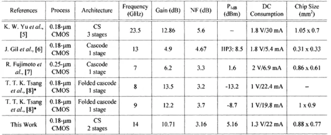
ofbetter than 10 dB and 3.2-dB NF at 14 GHz. Table I summarizes thepreviously reported CMOS LNAs operated above 7 GHz. Ourchipdemonstrates goodNF and reasonablesmall-signal gainatKuband.
II. MMIC PROCESS
This Ku-band LNA is
implemented by
commercialstandard0.1 8-,umMS/RFCMOS
technology
whichprovides
onepolylayerfor thegateof the MOS andsixmetal layers
for inter-connection
[91,
[10]. The substrate conductivity is approximately 10 S/m. With optimized CMOS technology and deep n-well, this technology providesfT
andfmAx
of better than 60 GHz and 55 GHz, respectively. High-Q inductors can be formed using the top AlCu metallization layer of2-pm
thicknesswithoutadditional masks. A MIM capacitorofIJF/jim2
hasbeendevelopedusingoxideinter-metaldielectric.
III. CIRCUIT DESIGN
Thetypical CMOS LNA topology is cascode with the source inductancedegeneration with the shortcoming ofthe relativehigh supplyvoltage. Sincethe drainof the common-source stage is terminated with the source of the common-gatedevice, the gainofthe common-source stage is nothigh
enough and the totalnoiseperformancewillbe degraded by the noiseofthe common-gate stage.
To achieve low supply voltage and avoid noise performance degradation, a common-source topology is
adoptedasinFig. 1. The input matchingconditionandnoise performance of an inductive degeneration topology with ideal inductorswas fully analyzed in
[131,
and the parasitic resistance was also considered. The input impedance isZm=s(Lg +Lj)+
Sc9s
I+Rg
+RLgl+RLl+C°"L,
g
Cgst1
(1)
where
C.,
is the gate-source capacitance andgml
is thetransconductance of transistor
Ml.
R.
is the effective gateresistance.
RLgl
andRL1
are the parasitic resistance ofthe inductorsLgiandL,1.
Thematchingcondition occurswhen02Cgs(Lg+
L)o
=1 (2)(3)
R =Rg
+RLg1+RRLI
+C LSgs
Atwo-stagetopologyis usedtosimultaneouslyoptimize
the gain andnoiseperformancesasinFig. 1. Thefirststage isdesigned for noise performance and the second stage is
designed forpowergain. The transistorsize ofthefirststage is
16Opmm/O.18gm,
and the second stage is the same.0-7803-9372-4105/$20.00@2005IEEE
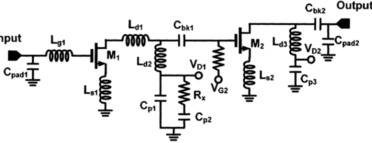
Ld1
Cbkl
cp2
Fig. 1. Schematic of the Ku-band CMOS LNA.The inter-stage is complex conjugate matched achieved by theinter-stageinductor
Ln
and the drain inductorLd2.
The inductance ofLn
andLd2
is 150 and 167 pH, respectively. Thebias currentof theinputstageis fedthroughthebypassnetwork, consists
Cp1,
C.2
andR,.
TheCpl
is design for in-bandbypass andCp2
for low-frequencybandbypass. TheR,
is placed to depress the low-frequency gain and prevent resonanceof bypass capacitor andeffective inductance of the bias line(bondingwireordcprobe). The outputimpedance matchingnetwork is shunt-inductorLB.
Since theoperationfrequency is Ku band,the parasitic capacitance of1/0 pads
must also be considered. The RFpads are implemented by
topmetal with bottomground-shieldingmetal. Thecomplete
schematicof the Ku-band LNA is inFig. I.Allinductorsare realized as planar inductors. For the drain bias networks,
resistor and capacitor networks are designed for providing
theRFshortcircuit and lowfrequencystabilityconcern. The circuit simulation was perfonned in the software,
Agilent ADS (AdvancedDesign System) [I1]. Themodels of the resistors and MIM capacitors are provided by the
foundry, and the S-parameters of the inductors were simulated by the full-wave EMsimulator, Sonnet [12]. Fig.
2 presents the chip photoof the Ku-band CMOS LNA, and thechipsize is 0.88x 0.77
mm2.
IV. MEASUREMENTRESULTS
The LNA is measured via on-wafer probing. The measured NF andsmall-signalgainareshown inFig.3. The NFisbetter than 3.2 dB from 14to 16 GHzwhile the
small-signal gain is higherthan 10 dBbetween 12.5 GHz and 15 GHz. Thebestmeasured NF andgainare3.1 dBat 15GHz and 11 dB at 13.5 GHz, respectively. The measured input
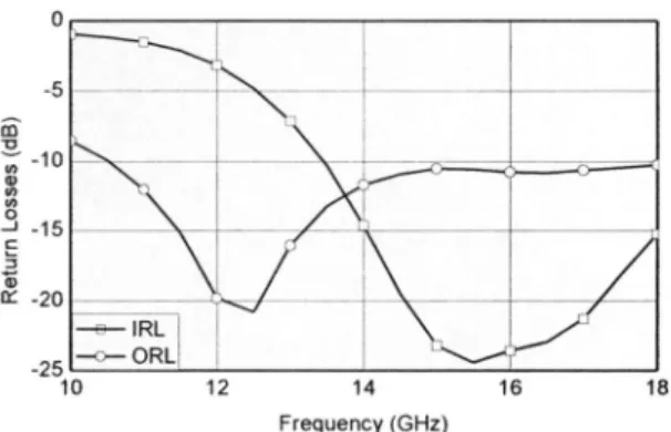
and output return losses are shown in Fig. 4. The input
return loss is better than 10 dBfrom 13.5 GHz to 18GHz, and the outputreturn loss is better than 10 dB from I1 GHz to 18 GHz. The powerperformance ofthisamplifieris also measuredat 14 GHz,and the measuredresults areshown in Fig. 5. The output andinputP1dB is about 5.2 dBm and -5
dBm, respectively. The measured input IP3 is 1.6 dBm, as shown in Fig. 6. The dc consumption is 1.3 V/I I mA for eachstage.
V. CONCLUSION
A CMOS LNA for Ku-band applications has been designed, fabricated and measured. This CMOS LNA demonstratesagain of betterthan 10 dB and a NF of better than3.2 dB from 14to 15GHz. The measured output
P1dB
is about 5.2 dBm and input IP3 is 1.6 dBm. The chip size includingall testing pads is 0.88 x 0.77mm2.ACKNOWLEDGMENT
This work is supported in part by NTU-TSMC Joint-Development Project, andNational Science Council (NSC 93-2752-E-002-002-PAE, NSC 93-221 9-E-002-024 and NSC93-2213-E-002-033). The chip is fabricatedby Taiwan SemiconductorManufacturing Company.
REFERENCES
[1] T.Yoshimasu,K.Sakuno, N. Matsumoto, E. Suematsu, T.Tsukao,
and T. Tomita,"A low-current Ku-band GaAsmonolithic image
rejectiondown-converter," IEEE J. Solid State Circuits, vol. 27, no.
IO,pp.1448-1451,Oct. 1992.
[2] K.Sakuno, T.Yoshimasu,N.Matsumoto, T.Tsukao, T.Nakagawa, E.Suematsu,andT.Tomita, "AminiaturelowcurrentGaAsMMIC downconverter for Ku-band broadcast satellite applications," in 1992 IEEE Microwave & Millimeter-wave Monolithic Circuits
SymposiumDigest, pp. 101-104,June1992.
[3] K. Yamanaka, K. Yamauchi, K. Mori, Y. Ikeda, H. Ikematsu, N.
Tanahashi,and T.Takagi, "Ku-band low noise MMIC amplifier with bias circuit forcompensation of temperature dependence and process variation," in 2002 IEEE International Microwave Symposium Digest, vol. 2, pp. 1427-1430, June 2002.
[41 [4]P. K.Ikalainen,L.C.Witkowski,and K.R.Varian, "Low-noise, low DC power linearamplifiers," in 1993IEEE Microwave & Millimeter-wave Monolithic Circuits Symposium Digest,
pp.159-162,June1993.
[5] K.W.Yu, Y.L.Lu,D.Huang,D.C.Chang, V.Liang, and M. F. Chang, "24 GHz low-noise amplifier in 0.18pm CMOS
technology," IEE Electronic Letters, vol. 39, Issue22,pp.
1559-184
Input
CpadlI
Cbk2
Output
1560,30 Oct. 2003.
[6] J.Gil,K.Han,and H.Shin,"13 GHz 4.67 dB NFCMOSlow-noise
amplifier," IEEElectronicLetters, vol. 39,Issue14,pp.1056-1058,
10July2003.
[7] R. Fujimoto, K. Kojima, and S. Otaka, "A 7-GHz I.8-dB NF CMOS low-noiseamplifier," IEEE J. Solid StateCircuits,vol.37,
no.7,pp.852-856, July2002.
[8] T.K. K.Tsang,and M. N.El-Gamal,"Gain controllableverylow
voltage(<I V)8-9GHzintegrated CMOS LNAs," in 2002IEFE RadioFrequencyIntegratedCircuitsSymposium Digest,pp.
205-207,June 2003.
[9] H. M.Hsu, J. Y.Chang, J.G. Su, C. C. Tsai, S. C.Wong, C. W.
Chen,K. R.Peng, S.P.Ma, C. H.Chen, T.H.Yeh,C.H.Lin,Y. C.
Sun,and C. Y.Chang,"A0.18-pmfoundryRFCMOStechnology
with 70-GHz ft for single chipsystemsolutions," inIEEE MTT-S Int.MicrowaveSymp. Dig.,vol.3,pp.1869-1872,2001.
[10] C. H.Diaz,etal.,"A0.18-pmCMOSLogic Technologywith Dual Gate Oxide and Low-k Interconnect for High-Performance and Low-Power Applications," IEEE VLSI Tech. Symp., pp. 11-12,
1999.
[111 AdvancedDesign SystemUser's Guide, AgilentTechnologiesInc.
[12] Sonnet user'smanual, Sonnet Software, Inc.
[13] D. K.Shaffer,and T.Lee,"A 1.5-V, 1.5-GHz CMOS low noise
amplifier,"IEEE J.Solid-StateCircuits, vol. 32,pp.745-759,Jun
1997
[14] G.Girlando,T.Copani, S.A.Smerzi,A.Castorina, and Palmisano,
"A 12GHz siliconbipolarreceiver fordigital satellite applications,"
ISSCCDig.Tech.Papers,pp.276-277, Feb. 2004.
a: *0 0 -E I F~~~~ -15 -20 -0-lo 12 14 16 18 Frequency (GHz)
Fig.4. Measuredinput and output returnlosses of the Ku-band CMOS LNA. La 0 a6 t0 -25 -20 -15 -10 -5 0 Input Power(dBm)
Fig.5.Measuredoutputpower versusinputpowerofthe LNAat14 GHz.
Fig. 2. Chip photo oftheKu-band CMOS LNA, and the chip size is 0.88x
0.77mm2.
m
8
r--____ _,__
6 _.Fe
-NF
0-o-GaiIIm
10 11 12 14 15 11 20 10 ~- 0 E co El-10 i0-20 -30 0-40 -50 -eo -2 -15 -10 -5 Input Power (dBm) 0 5
D
Fig. 6. Measured IP3.
Frequency (GHz)
Fig.3.MeasuredNFandsmall-signal gain ofthe Ku-band CMOSLNA.
185
Fundamental-1
1/
1
fM
Z
===~~,
10 10 D--- D- D C- QN-5__ 0__ 1 -5 0-1--10 __co.
-15 -20 -25 -30 out -35 in -45 -40 -35 -16 laTABLE 1. THE PREVIOUSLY REPORTED CMOS LNAsOPERATEDABOVE 7GHz.
References Process Architecture Frequency Gain(dB) NF(dB) PdB DC ChpSz
__(dB onsu mnption (m ')
K. W. Yueta!., 0.18-pm Cs
23S5
12.86 5.6S1.8V/30rnA
10i:x07
[51 CMOs 3stages 235 1.6 56- 18V0mA .5x07
J.Gil eta.
[6]|
0. 18-pmCMOsCascode
Istage 13 4.9 4.67 11P3: 8.5 1.8V/5.4
mA 0.31 x0.33R. Fujimotoet 0.25-pm Cascode 7 6.2 3.3 1.6 2V/6.9mA 0.86x0.61
al..17] CMOS I stage
T.T. K. Tsang 0.18-pm Foldedcascode 8 13.5 3.2 -13.2 1V122.4mA
etal.,181* CMOS 1 stage
T. T. K.Tsang 0.18-pm Foldedcascode 9 12.2 3.7 -8.7 1
V/19.8
mA 1x 0.9etal.,
[8]*
CMOS 1stageThis Work
0.1I
8-pm
CS
14 10.71 3.16 5.16 1.3V/22mA0.88
x0.77CMOs 2stages
*:variablegain amplifier. gaincontrol range> 10dB