國 立 交 通 大 學
光 電 工 程 研 究 所
碩士論文
利用簡單熱氣相沉積法成長之氧化銦奈米
結構之相關特性研究
Research on Indium Oxide nanostructures
and their characterizations grown by simple
thermal vapor deposition
研
研
究
究
生
生
:
:
朱
朱
家
家
璞
璞
..指
指
導
導
教
教
授
授
:
:
郭
郭
浩
浩
中
中
教
教
授
授
盧
盧
廷
廷
昌
昌
教
教
授
授
中
中
華
華
民
民
國
國
九
九
十
十
六
六
年
年
七
七
月
月
利用簡單熱氣相沉積法成長之氧化銦奈米結構之相關特性研究
Research on Indium Oxide nanostructures and their
characterizations grown by simple thermal vapor deposition
研究生:朱家璞 Student: Chia-pu Chu
指導教授:郭浩中 教授 Advisor: Prof. Hao-chung Kuo
盧廷昌 教授 Prof. Tien-chang Lu
國 立 交 通 大 學
光電工程研究所
碩 士 論 文
A Thesis
Submitted to Institute of Electro-Optical Engineering College of Electrical Engineering and Computer Science
National Chiao Tung University in Partial Fulfillment of the Requirements
for the Degree of Master
In
Electro-Optical Engineering
July 2007
利用簡單熱氣相沉積法成長之氧化銦奈米結構之相關特性研究
研究生:朱家璞 指導教授:郭浩中 教授 盧廷昌 教授交通大學光電工程研究所
摘要
在 本 篇 論 文 中 , 主 要 是 探 討 利 用 熱 氣 相 沉 積 方 法 並 且 推 測 是 藉 由 vapor-solid 與 vapor-liquid-solid 成長機制下所形成之氧化銦奈米結構相關 特性的研究,在我的實驗中成功形成了三種奈米結構,分別為氧化氮銦奈米顆 粒、氧化銦奈米串鏈、以及似水果枇杷狀的氧化銦奈米結構,在特性分析中,包 含了結構與光學特性上的相關研究。結構及相關成分性的研究包含了掃描式電子 顯微鏡圖像、高解析度穿透式電子顯微鏡圖像、能量散佈光譜、x 光繞射圖…, 在發光特性方面,所利用的是光激發螢光光譜的分析。 在第一部分的氧化氮銦奈米顆粒中,奈米顆粒推測是以 VS 的成長機制形成 的八面體結構,以成長溫度在攝氏 600 度至 900 度形成各個尺寸從 50 奈米至 1 微米間的奈米顆粒,並可在能量散佈光譜中,驗證此奈米結構的存在成分,並在 光激發螢光光譜中,可以看出此奈米顆粒的發光範圍可以涵蓋整個紅光波段。第 二部分所形成的氧化銦奈米串鏈,亦是藉由類似方式所形成,僅別於利用直徑約 20 奈米的金奈米粒子先形成長於基板表面,形成奈米串鏈與基板的嫁接,而尺 寸介於 20 奈米至 100 奈米間的奈米顆粒因而相連成串鏈,並且在研究熱退火過 程中,發現熱退火對於此奈米結構在光學及結構特性上皆有改善。由於欲形成奈 米柱狀的氧化銦奈米結構,因此以金奈米粒子最為觸媒,而形成最後一部分的枇 杷狀氧化銦奈米結構,在高解析度穿透是顯微鏡圖像中,可以看出以 VLS 成長的 證據,在此部分,我分別改變通入氧氣流量及成長溫度,來研究這兩變因對於結 構及發光特性上的影響,結果發現在不同成長溫度下,對於發光波段之調變,有 明顯助益,波長可從 410 奈米延伸至 620 奈米。Research on Indium Oxide nanostructures and their characterizations grown by simple thermal vapor deposition
Student: Chia-pu Chu Advisors: Prof. Hao-chung Kuo Prof. Tien-chang Lu
Institute of Electro-Optical Engineering, National Chiao Tung University
Abstract
In this thesis, I mainly report on the growth and the characterizations of relevant Indium Oxide nanostructures via the suggested Vapor-Solid (VS) and Vapor-Liquid-Solid (VLS) mechanism by simple thermal vapor deposition. In my experiments, I have successfully synthesized three kinds of nanostructures: they are Indium-OxyNitride nanoparticles, Indium Oxide nanochains, and loquat-like Indium Oxide nanostructures sequentially. Moreover, I have characterized the nanostructures structurally and optically. The research on the nanostrucutres’ structures and the composition were carried out by Scanning Electron Microscope (SEM), High Resolution Transmission Electron Microscope (HRTEM), Energy Dispersive Spectroscopy (EDS), and X-ray Diffraction (XRD)…. On the optical emission part, I utilized Photoluminescence (PL) to investigate the emission wavelength.
In the first section of my experiments, Indium-OxyNitride nanoparticles, they are octahedrons suggested to be formed via the VS mechanism dispersed on the Silicon substrate, ranging from 50 nm to 1 um in size grown from 600 degrees to 900 degrees in Celsius. The composition is also verified by the EDS apparently. The PL shows the emission wavelength spans the whole red region. In the second section, Indium Oxide nanochains were formed in the similar way; the difference lies only in utilizing 20 nm gold nanoparticles as the catalysts and the linkers for first nanoparticle growth on the top of the Silicon substrate. And then more and more nanoparticles connected to one another sequentially by the adhesion between each other. Besides, after annealing the as-grown samples, the structural and optical quality were both improved accordingly. Owing to the objective of forming Indium nanorods or nanowires, gold nanoparticles were still introduced as the catalysts for favoring the VLS mechanism to take place. As a result, the loquat-like nanostructures were formed. And the TEM images validated the growth via the VLS mechanism. In this section, I adjusted the Oxygen flow and the growth temperature separately as factors to examine the impact on their characteristics of structure and emission wavelength. Finally, it was found the growth temperature impacted obviously on wavelength tuning. The wavelength shifted from 410 nm to 620 nm as the growth temperature increased from 5000C to 900 C. 0
Acknowledgement
Looking back for the past six years at NCTU inclusive of my undergraduate and graduate session, I am still indebted and grateful to whom I had shared the great moment with. More than that, I cherish and miss the moment to learn at class and study with my buddies. Though it was not always enjoyable in the graduate life, I reaped so much as I basked in the highly aggressive and competitive atmosphere of semiconductor laser lab. Time passes, and it comes to the terminal of my academic journey at NCTU. While I am so fortunate and blessed to be instructed by my advisors: S. C. Wang, H. C. Kuo, and T. C. Lu; I have admired the scholarly charisma, affable personality, and wholehearted endeavor out of them.
Besides, I appreciate my baseball teammate, the third baseman also my senior, Lazywind. He is such a nice guy with a good temper and care for my research work. We are just like buddies that no barricades could baffle us from working harmoniously. R. C. Gao, my optical measurement partner, is a ravishing and typical Hakka girl with a kind heart along with the extreme obedience to any task designated by our senior. I appreciate the kindness and gentleness out of her, even I feel so obliged to her help with u-PL measurement. M.J. Tsai, a partner for man,s talk, is a very nice friend to share anything with. Despite the research field, we shared an unforgettable summer on the soccer field for watching World Cup 2006 on TV live relay. Sounds crazy, we missed almost no games. My buddies, B44 guys inclusive of TMY; I have enjoyed a wonderful year with you all. Thanks Gandpa Hua for his help on AUTOCAD drawings, Yuan,s patience with my injured knee while playing basketball, TMY,s motorbike and his P2P links to watch C. M. Wang,s pitch on-line and Brother Chang,s snacks which were always ready for me in his drawer. I am much obliged to any of my seniors, classmates, and juniors who have helped me a lot to finish the research work. Nevertheless, I have to apologize to ones I have not mentioned in the preceding.
Eventually, all I want to say is thank you GOD for paving a so fabulous and exuberant path to me. Sometimes it was challenging and thorny, however, you arranged angels beside me to help me up. I miss the teachers here, my advisors of the lab, and anyone else we have shared great memories with. From them, I learned to do good things, to do them well, and to treasure them.
Content
Abstract (in Chinese)……….………...i
Abstract (in English )………..……….ii
Acknowledgement………...………iii
Content………...……….……….iv
List of Figures...vii
Chapter 1 Introduction and Motivation...1
1-1 Introduction to nanotechnology and low dimensional nanostructures……...1
1-2 Methods to form low dimensional Indium Oxide nanostructures…………..5
1-3 Properties of Indium Oxide and Indium Oxide compound semiconductors13 1-4 Review of thus far achievement in applications of Indium Oxide nanostructures………14
1-5 Motivation for my study on the growth and characterizations of Indium Oxide nanostructures……….20
Chapter 2 Theoretical background and experiment apparatus……….22
2-1 Growth mechanism of one-dimensional Indium Oxide……….22
2-2 Scanning Electron Microscope and Transmission Electron Microscope…...24
2-3 Energy Dispersive X-ray Spectroscopy (EDS) and Selected Area Electron Diffraction(SAED)………31
2-4 X-ray diffraction………34
2-5 Photoluminescence………38
2-6 Furnace………..…42
Chapter 3 Experimental Process, Results and Discussion………..43
3-1 Observation of strong red photoluminescence with broadband in indium oxynitride nanoparticles……….………43
3-1-1 Samples preparation and growth………..44
3-1-2 Structural and optical charaterizations……….…….…………....45
3-1-3 Summary………...………...……….50
3-2 Synthesis of In2O3 nanocrystal chains and annealing effect on their optical properties………..……….51
3-2-1 Samples preparation and growth…………..………....52
3-2-2 Structural and optical charaterizations……….52
3-2-3 Summary………..58
3-3 Thermally evaporated In2O3 nanoloquats with tunable broad band emissions………..59
3-3-1 Samples preparation and growth………...60
3-3-2 Structural and optical charaterizations………..61
Chapter 4 Conclusion……….66 Chapter 5 Future work and prospect………...68
List of Figures
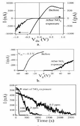
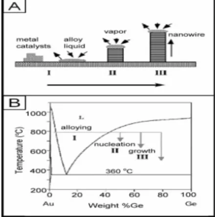
Fig.1-2-1. Schematic illustration of six different strategies that have been demonstrated for achieving 1D growth.………...7 Fig. 1-2-2 (a) Cross-section of Alumina template, unfilled. (b) Alumina template, filled with newly created nanowires. (c) Top view of Alumina template, filled with newly created nanowires………8 Fig. 1-2-3 Generalization of the Chemical Vapor Deposition process………10 Fig. 1-2-4 Generalization of the Vapor-Liquid-Solid process……….12 Fig. 1-4-1 (a) Current/Drain Voltage comparison graph at various gate voltages and room temperature. (b) Current/Drain Voltage comparison at a constant gate voltage (0 V) and varying temperatures………14 Fig. 1-4-2 (a) Current vs. Drain Voltage comparison with no gate voltage applied. The arrows indicate different scales - the before trend uses the left scale, and the after trend uses the right scale. (b) Current vs. Gate Voltage comparison with -.3 V applied to the drain. (c) Time response of the Indium Oxide nanowire under various concentrations of NO ………..16 2 Fig. 2-1-1 (A) Schematic illustration showing the growth of a nanowire via the VLS mechanism. (B) The binary phase diagram between Au and Ge, with the indication of the compositional zones responsible for alloying, nucleation, and growth………...23
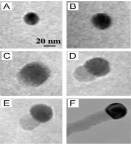
Fig. 2-1-2 The birth of a Ge nanowire on a Au nanocluster, as observed using in-situ
TEM………...………..24
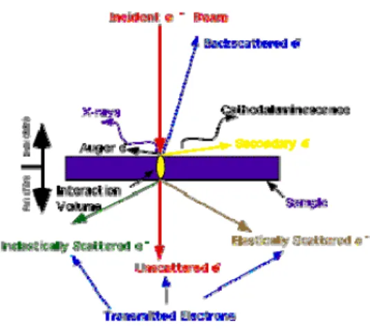
Fig. 2-2-1 Electron beam characterization techniques……….……...……….25
Fig. 2-2-2 Illustration of electron microscope system………..25
Fig. 2-2-3 Schematic of imaging of TEM………29
Fig. 2-4-1 Schematic of a basic X-ray diffractor setup………...………….36
Fig. 2-4-2 Deriving Bragg's Law using the reflection geometry and applying trigonometry……….………...…...36
Fig. 2-4-3 The unit cell of Body-Centered Cubic ………...37
Fig. 2-5-1 Schematic setup for PL system……….………..39
Fig. 2-5-2 The band diagram of possible routes to radiative recombination…...40
Fig. 2-6-1 Schematic of the furnace setup……...……….42
Fig. 3-1-1 (a) A typical SEM image of indium oxy-nitride nanoparticles with well-shape octahedron grown on a Si substrate. (b) EDS results of indium oxy-nitride nanoparticles………..………...69
Fig. 3-1-2 XRD results of indium oxy-nitride nanoparticles on Si (100) substrate. The numbers above the peaks correspond to the (hkl) values of the cubic structure……..70
Fig. 3-1-3 SEM images of indium oxy-nitride nanoparticles grown at different temperature. (a)-(d): 600, 700, 800, and 900 ℃………..71 Fig. 3-1-4 PL spectra of indium oxy-nitride nanoparticles grown at different temperatures for 30 min………...72 Fig. 3-1-5 PL spectrum of indium oxy-nitride nanoparticles grown at 900 for 150 ℃ min. The insert SEM image reveals the morphology of the nanoparticles…………..73 Fig. 3-2-1 (a)(b) Seclected area SEM images of In O2 3 nanochains grown on a Si substrate. (c) EDS results of In O nanochains………74 2 3 Fig. 3-2-2 (a) TEM bright-field image of part of a nanochain. (b) HRTEM image of the nanochain. (c) The corresponding selected area electron diffraction pattern…….75 Fig. 3-2-3 XRD pattern of the In O2 3 nanochains on Si substrate. The numbers above the peaks correspond to (hkl) values of the cubic structure……….76 Fig. 3-2-4 XRD ω-scan data from the In O nanochains……...………77 2 3
O
Fig 3-2-5 Room temperature PL spectra of In2 3 nanochains with He-Cd laser excitation of 325 nm……….78 Fig. 3-2-6 Transition and emission mechanisms for In2O nanochains……...……….79 3 Fig. 3-3-1 (a)(b) Photographs of real loquats. (c)~(f) SEM images of In O2 3 nanoloquats grown by using different oxygen flow rates of 50, 100, 150 and 200 sccm, respectively………...80
Fig. 3-3-2 (a)~(c) SEM images of In O2 3 nanoloquats grown by using different growth temperatures of 500 0C, 700 0C, and 900 0C, respectively………..81 Fig. 3-3-3 (a)(b) TEM images of the In2O3 nanoloquats tip. (c) High-resolution TEM images of part of the In O2 3 nanoloquats. (d) The corresponding selected area electron diffraction pattern of the In2O nanoloquats………82 3 Fig. 3-3-4 XRD pattern of the In2O3 nanoloquats grown in different oxygen flow rates (a) and different growth temperatures (b)………83 Fig. 3-3-5 Room temperature PL spectra of the In O2 3 nanoloquats grown by using different oxygen flow rates (a) and different growth temperatures (b)………84
Chapter 1 Introduction and Motivation
1-6 Introduction to nanotechnology and low dimensional nanostructures
Nobel laureate Richard Feynman predicted that by the year 2000 products would be built one molecule or one atom at a time. The basic idea of nanotechnology was stated in 1959 by the famous physical scientist in the lecture “There's Plenty of Room at the Bottom.” This was a truly bold vision because it would represent a new paradigm for manufacturing and constitute a fundamental economic shift analogous to a second industrial revolution. This shift is referred today as the "nanotechnology revolution," and many people consider Dr. Feynman’s quote the birth of nanotechnology..
The computer industry is just one example of the advantages related to miniaturization. Getting small is a means of increasing the power and value of diverse products and services in most industries. For instance, many advances in biotechnology and the development of new drugs are the direct result of miniaturization and utilization of novel materials. The computing power, diagnostic and research power increase as tools decrease in size. Getting small allows biotechnology companies and researchers to do more complex experiments in shorter periods of time, for less money, using less material. This greatly accelerates discovery and ultimately shortens the time from concept to market for new advanced drugs and
other products. Further, nanotechnology enables companies and researchers to design revolutionary new products using new materials and substances not accessible with other technologies.
Nanotechnology, loosely defined as the study of functional structures with dimensions in the 1-100 nanometer range, is emerging as a distinct and promising field of research. Certainly, many organic chemists have designed and fabricated such structures for decades via chemical synthesis. During the last decade, however, developments in the areas of surface microscopy, silicon fabrication, biochemistry, physical chemistry, and computational engineering have converged to provide remarkable capabilities for understanding, fabricating and manipulating structures at the atomic level.
Research in nanoscience is literally exploding, both because of the intellectual allure of constructing matter and molecules one atom at a time, and because the new technical capabilities permit creation of materials and devices with significant societal impact. The rapid evolution of this new science and the opportunities for its application promise that nanotechnology will become one of the dominant technologies of the 21st century.
making a single molecule. Often nanotechnologists wish to make arrays of identical or complex molecules, sometimes on a scale that will transcend the boundaries of the microscopic and approach the macroscopic. There are two different approaches to this end, 'top-down' and 'bottom-up.' The top-down approach is exemplified by scientists who build objects and molecular arrays using the techniques of scanning probe microscopy. The bottom-up approach is exemplified by investigators who design two- and three-dimensional chemical systems that cohere according to the rules of chemical interactions. The advantage of the top-down approach is its exquisite precision, but its disadvantage is its lack of extensive parallelism--it requires manipulating atoms and molecules practically one by one. In contrast, the bottom-up approach is massively parallel.
Two-dimensional (2D) nanosturctures (or quanum wells) [1] have been extensively studied by the semiconductor community because they can be conveniently prepared using techniques such as molecular beam epitaxy (MBE) [2]. Thanks to the efforts from many research groups, significant progress has also been made with respect to zero-dimensional (0D) nanostructures (or quantum dots) [3] in the past two decades. With quantum dots as a model system, a lot of intriguing chemistry and physics has been learned by studying the evolution of their fundamental properties with size [4]. Using quantum dots as active components,
various types of nanoscale devices have also been fabricated as prototypes in many research laboratories. Remarkable examples include quantum dot lasers [5], single-electron transistors [6], memory units [7], snsors[8], optical detectors [9], and light emitting diodes [10]. In recent, one-dimensional (1D) nanostructures such as nanowires, nanorods, nanobelts, and nanotubes have also become the focus of intensive research due to their unique applications in mesoscopic physics and fabrication of nanoscale devices. 1D nanostructures provide a good system to investigate the dependence of electrical and thermal transport or optical transition properties on dimensionality and size reduction also quantum confinement effect. They are also expected to play an important role as both interconnects and functional units in fabricating electronic, optoelectronic, electrochemical, and electromechanical devices with nanoscale dimensions.
In contrast to quantum dots and wells, the advancement of 1D nanostructures have been slow until very recently, since hampered by the difficulties correlated with synthesis and fabrication of these nanostructures with well-controlled dimensions, morphology, phase purity, and chemical composition. Although 1D nanostructure can now be fabricated by using a variety of nanolithographic techniques [11], such electron-beam and focused-ion-beam writing, and x-ray or extreme-UV lithography, further development of these techniques into practical routes to a large quantities of
1D nanostructures from a diversified range of materials, swiftly, and at acceptable low costs, still requires great ingenious efforts. On the contrary, unconventional methods based on the chemical synthesis (will be discussed in the following passage) might provide an alternative and intriguing course for generating 1D nanostructures in terms of material diversity, cost, throughput, and the potential for high-volume production [12].
1-7 Methods to form low dimensional Indium Oxide nanostructures
The essence of 1D nanostructure formation is about crystallization, a process hat has been delved into for hundreds of years. The evolution of a solid from a vapor, liquid, or solid phase comprises two fundamental steps: nucleation and growth. As the concentration of the building blocks of a solid becomes sufficiently high, they aggregate into small clusters or namely, the nuclei, through homogeneous nucleation. With a continuous supply of the building, these nuclei can serve as seeds for further growth to form larger structures. Though crystallization has been studied for such a long period, very little is known quantitatively about the process. Also, it’s generally accepted that the formation of a perfect crystal requires a reversible pathway between the building blocks on the solid surface and those in a fluid phases (i.e. vapor, solution, or melt). Theses conditions allow the building blocks to easily adopt correct position
in developing the long-range-ordered, crystalline lattice. Moreover, the building blocks also need to be supplied at a well-controlled rate to obtain crystals with a homogeneous composition and uniform morphology.
While developing a synthetic approach for generating nanostructures, the most significant issue to be addressed is the simultaneous control over dimensions, shapes, and the uniformity. In the past several years, multitudes of chemical methods have been reexamined or demonstrated as the “bottom-up” approach for generating 1D nanostructures with different level of control over these parameters. The following figure illustrates some of these synthetic strategies that contain 1) use of intrinsically anisotropic crystallographic structure of a solid to accomplish 1D growth (Fig. 1-2A); 2) introduction of a liquid-solid interface to reduce the symmetry of a seed (Fig. 1-2B); 3) use of various templates with 1D morphologies to direct the formation of 1D nanostructures (Fig. 1-2C); 4) use of supersaturation control to modify the growth habit of a seed; 5) use of appropriate reagents to kinetically control the growth rates of various facets of a seed (Fig. 1-2D); 6) self assembly of 0D nanostructures (Fig. 1-2E) and 7) size reduction of 1D microstructures (Fig. 1-2F).
Fig. 1-2-1. Schematic illustration of six different strategies that have been demonstrated for achieving 1D growth.
The following tips are demonstrating several feasible fabrication methods for Indium Oxide 1D nanostructures. The commonly used methods of fabrication are the Chemical Vapor Deposition (CVD) and the Vapor-Liquid-Solid (VLS) methods, with other less commonly used methods as well (consisting of electrodepositing Indium onto an Alumina template, then adding oxygen, or the method of rapidly heating Indium grains in a mixture of Argon and Oxygen). How these methods work, and their usefulness are explained below.
A. Electrodeposition
This method consists of what is basically described above: An Alumina (Al O
2 3)
template is fabricated by anodizing Aluminum (i.e. the Aluminum is electrically charged to about 40 V, making it the anode to a typically Platinum Cathode, in a
acidic electrolytic solution, to create the porous Alumina template of about 30 micrometers thick). After this, Indium Particles are put in the equation, dropped into the recently created Alumina template. The particles are small enough to fit into the template’s pores, and are pulled in and bonded together. After this, the now formed Indium nanowires are oxidized (that is, Oxygen is added into the system), creating Indium Oxide nanowires [13, 14].
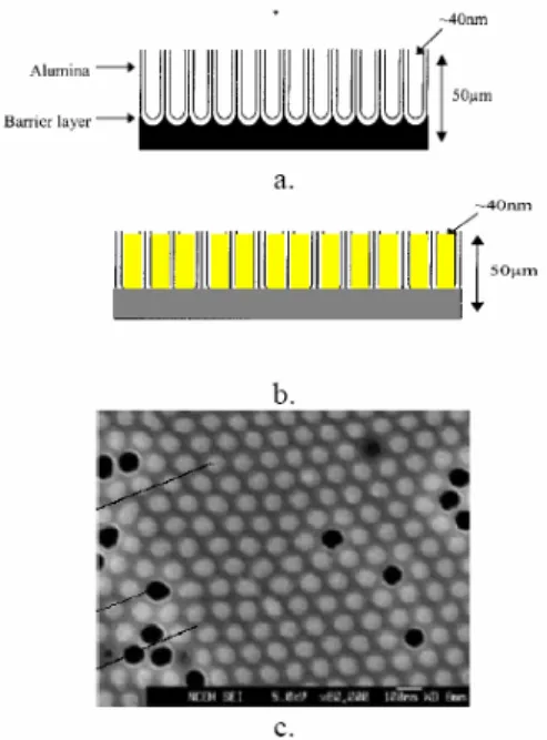
Fig. 1-2-2 (a) Cross-section of Alumina template, unfilled. (b) Alumina template, filled with newly created nanowires. (c) Top view of Alumina template, filled with newly created nanowires. Black holes refer to unfilled pores in the template white dots refer to filled pores, and the gray area in between dots is the Alumina template.
The strong points this technique makes lies in its possible high aspect ratio, along with pore size and packing density of the wires being controllable (as a function of acid strength and the amount of voltage used in the anodizing step). However, this technique can only create polycrystalline Indium Oxide nanowires, so other
techniques must be used in the fabrication of single-crystalline nanowires.
B. Rapid Heating
Through this process to create single-crystalline Indium Oxide nanowires, Indium grains (particles) are placed in an atmosphere consisting of a mixture of Argon and Oxygen (one such atmosphere consists of 90 % Argon and 10% Oxygen [15]). This atmosphere is maintained at a very high temperature (about 1030ºC [15]), and from there, using a vapor to solid approach (no catalyst is involved in this process, unlike the CVD approach [15]), the Indium grains combine with the Oxygen in the atmosphere and subsequently combine with other compounds as well to form the nanowires.
The advantage this method has is in no need for a catalyst, so further materials do not need to be brought into the equation. However, this method is rarely used anymore simply because of the fact that there is no way to control the diameter of the nanowires created. Diameters can vary greatly (from 40-120 nanometers [15]), so the need of a more controlled method is apparent, as this method is too varied for any scientific analysis.
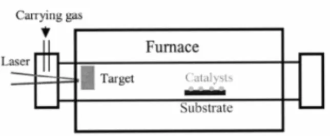
C. Chemical Vapor Deposition
This method is very similar to the previously explained method, but holds a few key differences. In this method, the Indium matter (which is introduced from a laser ablation process, which projects a laser onto a Indium Arsenic target, releasing Indium particles along the way due to the incident light [16]) is vaporized in a vacuum tube (similarly to the method above, as the temperature was kept at a very high temperature), then flowed into a specific containment area afterwards. After this, an Argon/Oxygen gas mixture is also flowed into this containment area. The Oxygen reacts with the Indium, creating Indium Oxide particles. Different to the method above, these molecules are then placed onto a Silicon substrate, laced with a Gold catalyst. From each Gold molecule, the nanowires grow radially outward, until the process cannot allow for more molecules on one nanowire. After all of this, the area is cooled down to allow for the solidification of the nanowires [17]..
Fig. 1-2-3 Generalization of the Chemical Vapor Deposition process.
In this process, laser ablation is used to release Indium particles from the target. These particles, along with an Argon/Oxygen mixture, are flowed into a high
temperature furnace. At the opposite end of the furnace resides a Silicon substrate, with Gold atoms as catalysts. The Indium Oxide molecules, formed earlier in the furnace, is attracted to the catalysts, and forms Indium Oxide wires from it [16].
The key differences between this process and the process described above are what make CVD perform better than its rapid heating counterpart, in the sense that diameter variance is much less (typically 30-50 nanometers [16]). However, even though the variance is down, there is still very little direct control over what diameter will be produced, which makes the following process much more widely used in the fabrication of Indium Oxide nanowires.
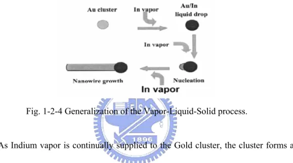
D. Vapor-Liquid-Solid
Vapor-Liquid-Solid (VLS) growing is a very sophisticated method, borrowing much from the Chemical Vapor Deposition process, in the fact that it uses the combination of things in vapor form to create the nanowires. Once again, Indium vapor is created using the laser ablation process on the Indium Arsenic target, which is introduced into the high temperature furnace (although there is no Oxygen present yet). However, this is where things get a bit different. Now, a Gold cluster is placed in the system, and is continually bombarded with the Indium vapor. From this continual feeding of the vapor, the Gold cluster forms into a Gold/Indium liquid drop (as the
temperature is high enough to vaporize Indium but not high enough to vaporize the combination of the two, just liquefying them), then the drop reaches supersaturation from all of the Indium, making the Indium particles grow out into a nanowire. After the Indium nanowire is created, Oxygen is then introduced, creating the single-crystalline Indium Oxide nanowire [13].
Fig. 1-2-4 Generalization of the Vapor-Liquid-Solid process.
As Indium vapor is continually supplied to the Gold cluster, the cluster forms a combination with the Indium, followed by the overabundance of Indium forming in a nanowire growth. Oxygen is then supplied to create the single-crystalline Indium Oxide nanowire.
From this process, nanowire diameter is directly controllable, as it is proportional to the size of the Gold cluster put in the system, and is basically equal to the diameter of the Gold/Indium combination. Therefore, creating consistent nanowires is now attainable, and as such, this is the most widely used method, especially when doing analysis on the properties an Indium Oxide nanowire contains [13].
1-8 Properties of Indium Oxide and Indium Oxide compound semiconductors
As far as the elements themselves go, Indium (element number 49 on the periodic table) is a fairly abundant metal, white and silvery in color, and produces a high-pitched sound when bent. A major application of Indium is to make low melting point alloys. Also notable is that Indium is a byproduct of the formation of Lead and Zinc, and many isolation processes (such as the electrolysis of Indium salts in water) are required to make Indium samples pure enough for electronic purposes [18]. Finally, plating applications exist for Indium due to its high resistance to corrosion, as well as it being used for doping semiconductors in transistor fabrication [19]. Oxygen (element number 8 on the periodic table) is a very abundant gas (which is colorless, but pale blue in a liquid state) that most life on the planet needs to live. About one fifth of the earth’s atmosphere is comprised of Oxygen, and Oxygen is well known to be a highly reactive element, and forms many compounds with other elements Finally, the combination of the two, Indium Oxide (In2O3), the compound of interest in the fabrication of Indium Oxide Nanowires, is a crystalline yellow solid, with a very high melting point (approximately 1913°C) and also known to be fairly dense as well (approximately 7180 kg/m³) [18]. Because of these properties, it is well suited to be used for electrical and optical applications (as it is an n-type semiconductor, but also can pass over 90% of visible light through it [20]). In addition, it’s a wide bandgap
material with the bandgap of around 3.5~3.6 Ev (340 nm). When it comes to such a wide bandgap material, it may intrigue people for its application on UV LEDs’ and white illumination.
1-9 Review of thus far achievement in applications of Indium Oxide nanostructures
A. Transistor Applications
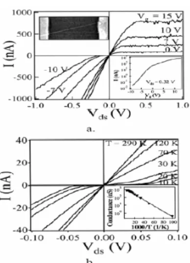
Because of the Indium Oxide nanowire’s semiconductor nature, it is well suited for use in field effect transistor applications. At the University of Southern California, testing was conducted using 10-nanometer diameter Indium oxide nanowire as a bridge between two metal electrodes (indicating the source and drain) over a Silicon substrate (creating a FET with a 3 micrometer channel) [13]. Results of such testing can be seen below:
Fig. 1-4-1 (a) Current/Drain Voltage comparison graph at various gate voltages and room temperature. (b) Current/Drain Voltage comparison at a constant gate voltage (0
V) and varying temperatures.
From the figures above, one can see that the Indium Oxide nanowire functions well as a gate for a field effect transistor application, as the output graphs are very similar to that of a regular metal oxide semiconductor field effect transistor (Mainly because the Indium Oxide nanowire is a metal oxide semiconductor) [13].
B. Chemical Sensor Applications
The ability for Indium Oxide nanowires to detect certain things at room temperature, such as chemical compounds, has turned up in recent days as well, especially for detecting the gas with high electron-affinity. Because when exposing the Indium Oxide nanowires to such the atmosphere, the electrons flowing near the surface of nanowires could be easily captures by the gas and effect would also be observed from the I-V measurement due to the slump of conductivity. From the same research team at the University of Southern California, the nanowire transistors created for the above application turned up again in this application. The transistors were placed in a vacuum area (to avoid impurities coming in), and the nanowire’s conductance was monitored as a chemical compound (in this case, NO
2 or NH3) was diluted in Argon (an inert gas so it would not react with anything) or dry air and flowed in to the vacuumed chamber. Such a test produced these results for NO :
Fig. 1-4-2 (a) Current vs. Drain Voltage comparison with no gate voltage applied. The arrows indicate different scales - the before trend uses the left scale, and the after trend uses the right scale. (b) Current vs. Gate Voltage comparison with -.3 V applied to the drain. (c) Time response of the Indium Oxide nanowire under various concentrations of NO . 2
But what do these graphs say about the nanowire? In the first graph, before exposure to the compound, the trend exhibits that of a regular FET, with the well-defined linear and saturation regions. However, after the nanowire is exposed to the chemical compound, the conductance decreases dramatically, somewhere in the range of six orders of magnitude. If using such a difference in conductance as a basis, one could easily determine whether the compound was present or not. In the second graph, the chemical sensing properties of the Indium Oxide nanowire are reaffirmed, as well as other findings. As can be seen above, after exposure to the compound,
nanowire conductance is dramatically decreased. However, other findings pop up as well. For one, it is confirmed that the nanowire is an n-type semiconductor, as when the gate voltage negatively increased, the current drops, indicating a reduced conductance as well. Also, very important to note is the point where each of the curves flatten out, which more or less indicates the threshold point of the FET. As the compound is exposed, the threshold point increases from approximately –45 V to near +20 V, a very noticeable increase. In the final graph, one can note that the nanowire FET can detect even small concentrations of the compound; however the penalty the smaller compound gives is in the form of a much greater amount of time for the conductance to drop. From these experiments, the lowest concentration this FET was able to detect was 5 ppb. But why does the Indium Oxide nanowire act like this? This comes from NO
2 being an oxidizing gas (from it containing Oxygen in its compound). From this, the Indium Oxide readily adsorbs the molecules also captures the electrons near the nanowire’s surface, which will then leave less room for free electrons logically, since there is less room for free electrons to maneuver, the conductivity decreases [13].
From these proceedings, one can use the outputs after exposure to determine how much of a compound is present in the atmosphere (from looking at reaction time), what kind of compound, or compounds, exist (from shift in threshold point or drop in
conductance), and subsequently be able to thoroughly analyze your surroundings, knowing exactly what is around you. Compared to other sensors of the same nature, it is found that the sensitivity of the nanowire is much greater, as the difference of several orders of magnitude is better than the conventional sensor’s one or two orders of magnitude at the most [13].
C. Applied to Transparent Conductive Oxide
The followings are the items using Transparent Conductive Oxieds. · Touch panels
· Electrochromic, electroluminescent and LCD displays · Plasma displays
· Field emission displays · Heat reflective coatings · Energy efficient windows · Gas sensors
· Photovoltaics
Transparent conducting oxides (TCO) thin films are widely used in applications such as the transparent electrodes of flat panel displays, solar cells and touch panels. A combination of the p and n types TCO to form a p-n junction can result in qualities ideal for optoelectronics. Some transparent oxides such as ZnO are also known to be
candidates for diluted magnetic semiconductors, and have potential for applications in spintronic devices.
A number of materials such as tin-doped indium oxide (ITO), ZnO, and SnO2 are used in many optoelectronic devices. ITO is currently the most widely used TCO. However, as indium is a relatively scarce element, the cost for ITO production is high. The other drawback of ITO films is the lack of chemical stability. The indium of an ITO layer can diffuse into the organic materials, leading to the degradation of light emitting diode (LED). Tin doped indium oxide (In O2 3) is a transparent conducting material that is usually used in thin coating form. As a coating it is commonly deposited by methods such as electron beam evaporation or a range of sputtering techniques. The optical and electronic properties if ITO films are dependent on factors such as deposition parameters and starting materials. For instance, the film must contain a high density of charge carriers to conduct, however, the higher the density of charge carriers, the lower the transparency.
At present almost all TCO thin films are n-type semiconductors as it is extremely difficult to fabricate a p-type TCO semiconductor. However, it is crucial to fabricate the p-type in order to make active circuit components such as diodes in transparent circuits.
1-10 Motivation for my study on the growth and characterizations of Indium Oxide nanostructures
Because there are scarcely mention of the optical properties of Indium nanostructures with profound investigation and the direct utilization of such of the wide bandgap compound semiconductors, I am determined to be engrossed in the nanostructures growth along with their structural and optical characterization.
Indium oxide (In O2 3) is a very important compound semiconductor with a large band gap around 3.5 eV and has recently attracted much attention as a material for transparent electrodes in electronic devices such as liquid crystal displays [21], solar cells [22], sensing material [23] and nanowire technology [24]. In recent, the interest in the fabrication of In2O3 nanostructure has been mounting because of their possibility to applications for both nanoelectronic and optoelectronic devices and the passion to deal with unclear physical properties. Wang et al. obtained In O2 3 nanobelts by evaporation of In2 3O powders [25]. Li et al. grew In2 3 nanowires by a thermal O evaporation oxidation method with a catalyst by laser ablation [16]. Piqueras et al. grew In2O3 nanoarrows in thermally treated indium nitride for different annealing time [27]. Lao et al. observed nanochains and nanowire networks grown by a vapor transport and condensation method [28]. In spite of the accomplishment of an awful lot of In O nanostructures, the reports related to IndiumOxy-Nitride nanoparticles, 2 3
nanochains and even the unprecedented loquat-like nanostructures and their optical properties of In O2 3 are still limited and even unseen. Thus, my passion to delve into the investigation is ignited from this point.
Chapter 2 Theoretical background and experiment apparatus
2-1 Growth mechanism of one-dimensional Indium Oxide
Among all vapor-based methods, the VLS process seems to be the most successful for generating 1D nanostructures with single-crystallinity and in relatively large quantities. This process was originally developed by Wanger and coworkers to produce micrometer-sized whiskers in 1960s [28], and recently reexamined by Lieber [29], Yang [30], and many other research groups to generate nanowires and nanorods from a enormous variety of compound semiconductors. A typical VLS process starts with the dissolution of gaseous reactants into nanosized liquid droplets of a catalyst metal, followed by nucleation and growth of single-crystalline rods and then wires. The 1D growth is mainly induced and dominated by the liquid droplets, the sizes of which remain essentially unchanged during the entire process of wire growth. In this sense, each liquid droplet serves as a soft template to strictly constrain the lateral growth of an individual wire. As a major requirement, there should exist a good solvent capable of forming liquid alloy with the target material, ideally they should be able to form eutectic compounds.
However, one of the challenges confronted with the VLS process is the selection of an appropriate catalyst working with the solid material to be processed into 1D nanostructures. Presently, this is done by analyzing the equilibrium phase diagrams. It
has also been shown the analysis of catalyst and growth conditions can be substantially simplified by considering the pseu-binary phase diagram between the metal catalyst and the solid material of interest.
The following is a vivid example presented by Yang et al. [30], and all major steps involved in a VLS process are schematically illustrated in the Figure 2-1-1A with the growth of Ge nanorods as an example. According to the Ge-Au binary phase diagram (Figure 2-1-1B), Ge and Au form liquid alloys while the temperature is raised above the eutectic point (361 oC). Once the liquid droplet is supersaturated with Ge, nanowires or nanorods growth will begin to occur at the solid-liquid interface, as shown in Figure 2-1-2. Vapor pressure of Ge in the system has to be kept fairly low that secondary nucleation events will be thoroughly suppressed. Both physical methods (laser ablation, thermal evaporation, and sputtering) and chemical methods (chemical vapor transport and deposition) have been employed to generate the vapor species required for the growth of nanowires or nanorods, and no salient difference
structures produced by these methods.
was found in the quality of such nano
Fig. 2-1-1 (A) Schematic illustration showing the growth of a nanowire via the VLS mechanism. (B) The binary phase diagram between Au and Ge, with the indication of the compositional zones responsible for alloying, nucleation, and growth.
Figure 2-1-2 The birth of a Ge nanowire on a Au nanocluster, as observed using in-situ TEM. As
2-2 Scanning Electron Microscope and Transmission Electron Microscope
cident electro
following the increase in the liquid droplet (Ge-Au alloy) size during the Ge vapor condensation process, the droplet was supersaturated with Ge component. Simultaneously, a Ge nanowire grew out of this droplet and became longer as time elapsed.
Electron beam techniques are summarized in the Figure 2-2-1. In ns are absorbed, emitted, reflected, or transmitted and can, in turn, cause light or X-ray emission. For our frequent investigation, the secondary electrons emitted from the specimen and the incident electrons transmitting the specimen are specially intriguing among those generated or inherent electrons. Incident electrons can be focused, deflected, and accelerated by appropriate potentials; they can be sufficiently detected and counted, their energy and angular distribution can be measured, and they do not contaminate the sample or the vacuum system. As the so-called nondestructive measurement, these electron beam measurements do good to morphology characterization. However, because they are charged, they can cause samples charging that may distort the measurement.
Fig. 2-2-1 E iques
g. 2-2-2 Illustration of electron microscope system
The basic structure of both SEM and TEM is illustrated atop. The main spirit of the
A magnetic lens consists of a coil of copper wires inside the iron pole pieces. A current through the coils creates a magnetic field (symbolized by red lines) in the bore
lectron beam characterization techn
Fi
system is the electromagnetic optical system modulating the focus to form magnified image on the display.
of th
nce
I erform two different tasks:
1. Beam formation (condenser lenses in TEM
e pole pieces. The rotationally symmetric magnetic field is inhomogeneous in such a way that it is weak in the center of the gap and becomes stronger close to the bore. Electrons close to the center are less strongly deflected than those passing the lens far from the axis. The overall effect is that a beam of parallel electrons is focused into a spot (so-called cross-over).In a magnetic field, an electron experiences the Lorentz force F: The focusing effect of a magnetic lens therefore increases with the magnetic field B, which can be controlled via the current flowing through the coils. As it is described by the vector product, the resulting force F is perpendicular v and B. This leads to a helical trajectory of the electrons and to the magnetic rotation (image is rotated in respect of the object). Magnetic lenses influence electrons in a similar way as convex glass lenses do with light. Thus, very similar diagrams can be drawn to describe the respective ray paths. Consequently, the imaginary line through the centers of the lenses in an electron microscopes is called optical axis as well. Furthermore, the lens equation of light optics is also valid in electron optics, and the magnification of a lens is defined accordingly:
1/u + 1/v = 1/f Magnification M = v/u
f: focal length; u: object distance; v: image dista
n electron microscopes, magnetic lenses p
and SEM)
2 diffraction, intermediate, and
projective lenses in TEM
. Image formation and magnification (objective, ).
Right now, what I am going to discuss is the principle of useful electro characterization techniques used in my experiment:
n beam
1. Scanning Electron Microscopy:
An electron microscope utilizes an electron beam to produce a magnified image of the sample. There are three types of electron microscopes: scanning, transmission, and emission. In the scanning and transmission electron microscope, an electron beam incident on the sample produces an image while in the field-emission microscope the specimen itself is the source of electrons. SEM is similar to light microscopy with the exception that electrons are used instead of photons and the image is formed in the different manner. An SEM consists of an electron gun, a lens system, scanning coils, an electron collector, and a display (a CRT or an LCD), so does the TEM. The electron energy is typically 10-30 KeV for most samples, but for insulating samples the energy can be as low as several hundred eV. The use of electrons has two main advantages over optical microscopes: much larger magnifications are possible since electron wavelengths are much smaller than photon wavelengths and the depth of field is much larger. The image in an SEM is produced by scanning the sample with a focused electron beam and detecting the secondary or backscattering electrons. Electrons and photons are emitted at each beam location and subsequently detected. Secondary electrons form the conventional SEM image, backscattered electrons can
also form an image, X-rays are used to in the electron microprobe as to lead to the Energy Dispersive Spectroscopy, emitted light is known as cathodoluminescence, and absorbed electrons are measured as electron-beam induced current. All of these signals can be detected and amplified synchronously via the scanning coil and then forming magnified images on the display.
2. Transmission Electron Microscopy
With the similar structure and more powerful function compared with SEM, of specimen characterizations. There are three prim
The objective lens
TEM offers the in-depth perspective
ary imaging mode, listing as bright-field, dark-field, and high resolution microscopy. Image contrast does not depend very much on absorption, as it does in optical transmission microscopy, but rather on scattering and diffraction of electrons in the samples. Images formed using only the transmitted electrons are bright-field images and images formed using a specific diffracted are dark-field images. Few electrons are absorbed in the sample. Absorbed electrons lead sample to sample heating to change the sample during the measurement.
forms a diffraction pattern in the back focal plane with electrons scattered by the sample and combines them to generate an image in the image plane (1. intermediate image). Thus, diffraction pattern and image are
simultaneously present in the TEM. It depends on the intermediate lens which of them appears in the plane of the second intermediate image and magnified by the projective lens on the viewing screen. Switching from real space (image) to reciprocal space (diffraction pattern) is easily achieved by changing the strength of the intermediate lens. In imaging mode, an objective aperture can be inserted in the back focal plane to select one or more beams that contribute to the final image (BF, DF, HRTEM). In selected area electron diffraction (SAED), an aperture in the plane of the first intermediate image defines the region of which the diffraction is obtained. As shown in below.
Fig. 2-2-3 Schematic of imaging of TEM
In the bright field (BF) mode of the TEM, an objective aperture is placed in the back focal plane of the objective lens which allows only the direct beam to pass. In this case, mass-thickness e formation: thick areas, areas in which heavy atoms are enriched, and crystalline areas appear with dark
contr
In dark field (DF) images, one or more diffracted beams are allowed to pass the objective aperture. The direct beam is blocked by the aperture. In contrast to the direct beam, the diffracted beam has interacted strongly with the specimen, and often very useful information is present in DF images, e.g., about planar defects, stacking faults or pa
To obtain lattice images, a larger objective aperture has to be selected that allows many beams including the direct beam to pass. The image is formed by the interference of the diffracted beams with the direct beam (phase contrast). If the point resolution of the microscope is sufficiently high and a suitable sample oriented along a zon
The incident parallel electron wave interacts elastically while passing through the specimen, and the resulting modulations of its phase and amplitude are present in the electron wave leaving the specimen. The wave here, the object exit wave o(r), thus contains the information about the object structure. The objective lens performs
ast. In spite of the useful information obtainable from BF images, it should be mentioned that the interpretation of contrast is often impeded since these phenomena occur simultaneously.
rticle size.
e axis, then high-resolution TEM (HRTEM) images are obtained. In many cases, the atomic structure of the specimen can directly be investigated by HRTEM.
1. th
2-3 Energy Dispersive X-ray Spectroscopy (EDS) and Selected Area Electron Diffraction (SAED)
e Fourier transform (Fourier analysis) that creates the diffraction pattern of the object in the back focal plane and 2. the inverse Fourier transform (Fourier synthesis) that makes the interference of the diffracted beams back to a real space image in the image plane (lattice image).
EDS and SAED are two auxiliary function affiliated to SEM/TEM and TEM respectively. Both of them are used to characterize samples based on the constituents and structures. Energy dispersive X-ray spectroscopy (EDS or EDX) is an analytical tool predominantly used for chemical characterization. Being a type of spectroscopy, it relies on the investigation of a sample through interactions between light and matter, analyzing X-rays in its particular case. Its characterization capabilities are due in large part to the fundamental principle that each element of the periodic table has a unique electronic structure and, thus, a unique response to electromagnetic waves. The excess energy of the electron that migrates to an inner shell (in order to fill the newly-created hole) can do more than emit an X-ray. Often, instead of X-ray emission, the excess energy is transferred to a third electron from a
further outer shell, prompting its ejection. This ejected species is called an Auger electron, and the method for its analysis is known as Auger Electron Spectroscopy (AES). X-ray Photoelectron Spectroscopy (XPS) is another close relative of EDS, utilizing ejected electrons in a manner similar to that of AES. Information on the quantity and kinetic energy of ejected electrons is used to determine the binding energy of these now-liberated electrons, which is element-specific and hence allows chemical characterization of a sample. EDS is often contrasted with its microscale spectroscopic counterpart, WDS (Wavelength-Dispersive X-ray Spectroscopy). WDS differs from EDS in that it uses the diffraction patterns created by light-matter interaction as its raw data.
Selected area Electron diffraction, abbreviated as SAED, is a crystallographic
experimental technique that can be performed inside a transmission electron microscope (TEM).
In a TEM, a thin crystalline specimen is subjected to a parallel beam of high-energy electrons. As TEM specimens are typically ~100nm thick, and the electrons typically have an energy of 100-400 kiloelectron volts, the electrons pass through the sample easily. In this case, electrons are treated as wave-like, rather than particle-like (see wave-particle duality). Because the wavelength of high-energy
electrons is a fraction of a nanometer, and the spacings between atoms in a solid is only slightly larger, the atoms act as a diffraction grating to the electrons, which are diffracted. That is, some fraction of them will be scattered to particular angles, determined by the crystal structure of the sample, while others continue to pass through the sample without deflection.
As a result, the image on the screen of the TEM will be a series of spots -- the
selected area diffraction pattern, SADP, each spot corresponding to a satisfied
diffraction condition of the sample's crystal structure. If the sample is moved under the beam, bringing different sections of it under illumination, the arrangement of the spots in the diffraction pattern will change. If the sample is tilted, the same crystal will stay under illumination, but different diffraction conditions will be activated, and different diffraction spots will appear or disappear.
SAD is referred to as "selected" because the user can easily choose which part of the specimen to obtain the diffraction pattern from. Located below the sample holder on the TEM column is a selected area aperture, which can be inserted into the beam path. This is a thin strip of metal that will block the beam. It contains several different sized holes, and can be moved by the user. The effect is to block all of the electron beam except for the small fraction passing through one of the holes; by moving the
aperture hole to the section of the sample the user wishes to examine, this particular area is selected by the aperture, and only this section will contribute to the SADP on the screen. This is important, for example, in polycrystalline specimens. If more than one crystal contributes to the SADP, it can be difficult or impossible to analyze. As such, it is useful to select a single crystal for analysis at a time. It may also be useful to select two crystals at a time, in order to examine the crystallographic orientation between them.
As a diffraction technique, SAED can be used to identify crystal structures and examine crystal defects. It is similar to x-ray diffraction, but unique in that areas as small as several hundred nanometers in size can be examined, whereas x-ray diffraction typically samples areas several centimeters in size.
2-4 X
three-dimensional istribution (cubic, rhombic, etc.) of atoms in space. These are arranged so that they form a series of parallel planes separated from one another by a distance d, which
-ray diffraction
X-ray diffraction (XRD) is a versatile, non-destructive technique that reveals detailed information about the chemical composition and crystallographic structure of natural and manufactured materials. A crystal lattice is a regular
varies according to the nature of the material. For any crystal, planes exist in a number of different orientations --- each with its own specific d-spacing. When a monochromatic X-ray beam with wavelength lambda is projected onto a crystalline material at an angle theta, diffraction occurs only when the distance traveled by the rays reflected from successive planes differs by a complete number n of wavelengths. By varying the angle theta, the Bragg's Law conditions are satisfied by different
d-spacings in polycrystalline materials. Plotting the angular positions and intensities
of the resultant diffracted peaks of radiation produces a pattern, which is characteristic of the sample. Where a mixture of different phases is present, the resultant diffractogram is formed by addition of the individual patterns. Based on the principle of X-ray diffraction, a wealth of structural, physical and chemical information about the material investigated can be obtained. A host of application techniques for various material classes is available, each revealing its own specific details of the sample studied. Generally, XRD offers three types of scan: theta/2theta, rocking curve, reciprocal space mapping. The following is a basic XRD measurement setup derivation of Bragg’s law and an example for Body-Centered Cubic (BCC) characterization (Indium Oxide belongs to BCC.).
Fig. 2-4-1 Schematic of a basic X-ray diffractor setup.
.
Fig. 2-4-2 Deriving Bragg's Law using the reflection geometry and applying trigonometry. The lower beam must travel the extra distance (AB + BC) to continue traveling parallel and adjacent to the top beam. (2dSinθ=nλ)
x
z
y
a
a
a
Fig. 2-4-3 The unit cell of Body-Centered Cubic. The equation for the body-centered cubic structure is
1
d
2=
H
h
2+k
2+l
2L
a
2 (eq. 2-4-1)Combining with Bragg’s law (2dSinθ=λ) with eq. 2-4-1 yields
Sin
2θ
H
h
2+ k
2+l
2=
λ
L
24
a
2 (eq. 2-4-2)Rearranging eq. 2-4-2 gives
Sin
2θ =
λ
24
a
2H
h
2+k
2+l
2L
(eq. 2-4-3)
2-5 Photoluminescence
Photoluminescence is a process in which a chemical compound absorbs photons (electromagnetic radiation), thus transitioning to a higher electronic energy state, and then radiates photons back out, returning to a lower energy state. Technically, it is "luminescence arising from photoexcitation". The period between absorption and emission is typically extremely short, on the order of 10 nanoseconds. Under special circumstances, however, this period can be extended into minutes or hours.
Photoluminescence spectroscopy is a contactless, nondestructive method of probing the electronic structure of materials. Light is directed onto a sample, where it is absorbed and imparts excess energy into the material in a process called photo-excitation. One way this excess energy can be dissipated by the sample is through the emission of light, or luminescence. In the case of photo-excitation, this luminescence is called photoluminescence. The intensity and spectral content of this photoluminescence is a direct measure of various important material properties.
Ultimately, available chemical energy states and allowed transitions between states (and therefore wavelengths of light preferentially absorbed and emitted) are determined by the rules of quantum mechanics. A basic understanding of the principles involved can be gained by studying the electron configurations and
molecular orbitals of simple atoms and molecules. More complicated molecules and advanced subtleties are treated in the field of computational chemistry.
The following (Figure 2-5-1) is the schematic setup for PL system with a He-Cd operating at 25mW at the line of 325 nm.
Fig. 2-5-1 Schematic setup for PL system.
Hereby, I am going to introduce some fundamental transitions usually occur in the compound semiconductors, especially oxide compounds.
Because samples is excited with an optical source, typically a laser enrggy > Eg which generates electron-hole pairs (ehps), recombining by one of several mchanisms. Photons are emitted for radiative recombination. And photons are not emitted for nonradiative recombination in the bulk or at the surface. Some of the photons may be absorbed in the sample, provided the photons are directed to the back surface may be reflected and emitted. The photon energy is dependent on the recombination process, illustrated in the figure below (Fig. 2-5-2).
Incident photon Eg Ex E D EA (a) (b) (c) (d) (e) (f) Incident photon Incident photon Eg Ex E D EA (a) (b) (c) (d) (e) (f)
Fig. 2-5-2 The band diagram of possible routes to radiative recombination. Band-to-band recombination (Fig. 2-5-2 (b)) dominates at room temperature but it is rarely observed at low temperatures in materials with small effectives according to the large electron orbital radii. Nevertheless, when a photon generates an ehp, Coulomb attraction can result in the formation of excitonic state (a kind of excited state beneath the conduction band in the midst of the forbidden gap)in which an electron and a hole remain bound to one another. This kind of two elementary particles interaction is referred to a free exciton. Simply put, the electron hole pair binding leads to an exciton as shown in (Fig. 2-5-2 (c)). Its energy is less than the bandgap energy by Ex (excitonic binding energy). An exciton can move freely through the crystal, but because it’s a bound ehp, both electron and hole move simultaneously with each other and neither photoconductivity nor current takes place. However, a free hole can combine an electron on a neutral donor (Fig. 2-5-2 (d)) to
form a positively charged excitonic ion or the so-called donor bound exciton. The electron bound to the donor travels in a wide orbit about the donor. Likewise, electrons combining with a hole on neutral acceptors also form acceptor bound excitons, see Fig. 2-5-2 (e). Simply stated, as long as the semiconductor is less pure, the bound exciton recombination dominates over free exciton recombination. Let’s consider some indirect bandgap materials, though they don’t emit photons easily, once they emit the emissive energy must comply with the inclusion of phonon energy. That is, emissive energy = Eg-Ex-Ep, where Ep is the phonon energy. Ultimately, I have to combine all the conditions, i.e. the semiconductor is filled with impurity states. In order to give the simple case, I take only one donor and one acceptor into account (fig. 2-5-2 (f)). In this case, an electron on a neutral donor can recombine with a hole on a neutral acceptor, and this is the well known donor-acceptor (D-A) recombination. The emissive energy should be modified by the Coulomb attraction between donors and acceptors. Hence, the emissive energy becomes:
Eg-(EA+ED)+q2/4Πεr
where r is the distance between a donor and an acceptor. To be noted, the emissive photon energy can be higher than the bandgap in the heavily doping condition.
2-6 Furnace
This is a furnace with two-zone temperature controllers. And there are two kinds of gases provision. One is Nitrogen and the other is Oxygen. Attached to the end of the tube is a mechanical pump, which can exert itself to exhaust the air inside the quartz tube to the extent of 0.01 Torr. In my experiments, my samples were grown via the VLS and VS mechanism.Thus, preparing substrates with gold nanoparticles as catalysts was the first step. The research is in the scope of semiconductor nanostructure characterization and optical characteristics analyses. Looking forward to form oxide compound semiconductor nanostructures is substantially achieved. The following chapter will discuss profoundly about the product of my furnace and the characterization results. Below the passage is the schematic figure of the furnace.
+O2
Chapter 3 Experimental Process, Results and Discussion
Because my research is based on structural and optical characteristics of the compound semiconductor of Indium Oxide nanostructures, the following three main studies will be discussed hereafter. Since I want to form nanowire like structure, I start with Vapor-Solid technique to Vapor-Liquid-Solid technique in order to accomplish the goal and analyze the relevance. In addition, I place each of them in the section of 3-1, 3-2 and 3-3 individually. And the titles of these three sections are named after the distinct morphologies and optical emissive properties. We could see as follows,
3-1 Observation of strong red photoluminescence with broadband in indium oxynitride nanoparticles
3-2 Synthesis of In2O3 nanocrystal chains and annealing effect on their optical properties
O nanoloquats with tunable broad band emissions 3-3 Thermally evaporated In2 3
In each section, the content will begin with the samples preparation, results of all the characterizations and wind up with the discussion and conclusion of the phenomena of these nanostructures exhibit structurally and optically.
3-1 Observation of strong red photoluminescence with broadband in indium oxynitride nanoparticles
nitrogen atmosphere using a method involving a thermal evaporation of pure indium in a two-zone reactor. Nanoscale compositional analysis by energy dispersion spectrum shows the existence of indium oxy-nitride compound. X-ray diffraction analysis further confirms high crystallization and nitrogen atoms existence within the nanoparticles. Scanning electron microscopy investigations shows shape transformation from amorphous sphere to well-shaped octahedron with an average nanoparticle size from 50 nm to 1 µm when growth temperature of substrate increased from 600 to 900 °C. Photoluminescence study was performed on indium oxy-nitride nanoparticle samples grown at different temperatures. The emission intensity increases with growth temperature suggesting the formation of high quality indium oxy-nitride nanoparticles with increasing temperature. It was observed that these nanoparticles grown at 900 ℃ could emit a strong photoluminescence spectrum centered around 700 nm with a board full width at half maximum of about 250 nm, spanning the whole red band.
3-1-1 Samples preparation and growth
The experimental setup for synthesis of indium oxynitride nanoparticles is depicted
schematically in the experimental apparatus section. The starting material, 3 g indium metal, was placed in a quartz boat located inside an 8 cm diameter quartz tube reactor,