國
立
交
通
大
學
電子工程學系 電子研究所
博 士 論 文
雙重電漿處理技術應用於具高介電常數閘極絕緣層的金屬-絕
緣層-半導體電容及低溫多晶矽薄膜電晶體之特性研究
Investigation of Dual Plasma Treatment Technology on MIS Capacitor
and Low Temperature Polycrystalline Silicon Thin Film Transistor with
High-κ Gate Dielectric
研 究 生:張庭嘉
指導教授:張國明 教授
鄧一中 教授
雙重電漿處理技術應用於具高介電常數閘極絕緣層的金屬-絕
緣層-半導體電容及低溫多晶矽薄膜電晶體之特性研究
Investigation of Dual Plasma Treatment Technology on MIS Capacitor
and Low Temperature Polycrystalline Silicon Thin Film Transistor with
High-κ Gate Dielectric
研 究 生:張庭嘉 Student:Ting-Chia Chang
指導教授:張國明 Advisor:Kow-Ming Chang
鄧一中 I-Chung Deng
國 立 交 通 大 學
電子工程學系 電子研究所
博 士 論 文
A DissertationSubmitted to Department of Electronics Engineering and Institute of Electronics
College of Electrical and Computer Engineering National Chiao Tung University
in partial Fulfillment of the Requirements for the Degree of
Doctor of Philosophy in
Electronics Engineering
August 2012
Hsinchu, Taiwan, Republic of China
i
雙重電漿處理技術應用於具高介電常數閘極絕緣層的金屬-絕緣層-半導體電容及低溫多晶矽薄膜電晶體之特性研究
研究生:張庭嘉 指導教授:張國明 博士 研究生:謝智仁 指導教授:鄧一中 博士 國立交通大學 電子工程學系電子研究所 中文摘要 閘極長度及閘極氧化層的快速微縮會產生過大的閘極穿隧漏電流及元件可 靠度的問題,使用高介電常數材料取代傳統閘極二氧化矽可以有效解決此問題, 高介電質材料可以在較大的物理厚度下仍然維持較低的等效氧化層厚度,進而降 低閘極的穿隧漏電流並且維持較好的元件特性。在過去有許多論文曾經用電漿氮 化或電漿氟化處理對高介電常數材料薄膜使其達到較佳的特性,電漿氮化及電漿 氟化對於提升元件特性各有其優點,在本篇論文中,我們提出雙重電漿處理的方 式,結合沉積高介電薄膜前的電漿氟化處理及沉積後高介電薄膜後的電漿氮化處 理二種優點,並將此技術應用在具高介電材料的金屬-絕緣層-半導體電容及低溫 多晶矽薄膜電晶體結構上,以期結合兩種電漿處理之優點以更進一步提升元件的 電特性及可靠度。 首先,我們將雙重電漿處理技術應用具二氧化鉿的金屬-絕緣層-半導體電容 結構上,並探討其電特性及可靠度,並且分析其電流傳導機制。根據結果顯示, 經過雙重電漿處理的樣品均有顯著的改善,包括電容密度的提升、漏電的降低、ii 遲滯現象的改善,雙重電漿處理可以有效消除介電質薄膜中的缺陷、消除表面狀 態的數目、提升元件可靠度。另外,經雙重電漿處理後之二氧化鉿電容器,其漏 電流機制主要是由三種漏電機制所主導,分別是蕭基發射(Schottky emission)主 導中低電場, 弗崙克爾-普爾發射(Frenkel-Poole emission)主導於中高電場以及 福勒-諾德海姆穿隧(Fowler-Nordheim tunneling)主導於高電場。 其次,我們也將雙重電漿技術應用在具氧化鉿鋁之金屬-絕緣層-半導體電容 結構上,根據實驗結果,雙重電漿處理一樣可以有效提升其電特性及可靠度,改 善介面品質,增加其崩潰電壓。 最後,我們將電漿處理技術應用在多晶矽薄膜電晶體上,希望藉由雙重電漿 電漿處理可以鈍化二氧化鉿高介電常數材料內的氧空缺與基板的表面缺陷,亦可 修補多晶矽薄膜通道的缺陷,結果顯示,經過雙重電漿處理的樣品,臨界電壓(Vth)、 次臨界擺幅(S.S.)、轉導(Gm)、載子遷移率(μeff)都可以很有效的改善,表面狀態 數目(Dit)及多晶矽中的缺陷密度(Ntrap)也有效的降低。另外經由低頻雜訊(1/f noise or flicker noise)的量測可發現經過雙重電漿處理過的元件其表現出來的雜訊較低, 表示其介面及通道缺陷可以有效被修補。藉由可靠度的分析,包括給予閘極正偏 壓應力(PBS)、閘極負偏壓應力(NBS)、閘極正偏壓高溫應力(PBTI)、熱載子應力 (HCS)可觀察到介面層之陷阱能態密度(ΔNit)及氧化層缺面密度(ΔNot)。結果顯示, 經過雙重電漿處理過的樣品表現出較佳的元件電特性、較強的應力抵抗能力並提 升元件的可靠度。
iii
Investigation of Dual Plasma Treatment Technology on MIS
Capacitor and Low Temperature Polycrystalline Silicon
Thin Film Transistor with High-κ Gate Dielectric
Student:Ting-Chia Chang Advisors:Dr. Kow-Ming Chang
Student:Chih Ren, Hsieh AdvDr. I-Chung Deng
Department of Electronics Engineering & Institute of Electronics National Chiao Tung University
Hsinchu, Taiwan R.O.C.
Abstract
The aggressive shrinking of the gate length and gate dielectric thickness accompanies excessive leakage current and reliability problems. To solve these problems, a major solution is to replace the traditional SiO2 or SiON by High-dielectric-constant (high-κ) material. The improvement in the electrical characteristics of HfO2 thin film with plasma nitridation process or plasma fluorination process has also been examined. In this dissertation, dual plasma treatment, CF4 pre-treatment and nitrogen post-treatment, was performed on HfO2 MIS capacitor and low temperature polycrystalline silicon (LTPS) thin film transistors (TFTs).
First, dual plasma, CF4 pre-treatment and nitrogen post-treatment, treatments were performed on HfO2 MIS capacitor. We examine electrical characteristics,
iv
reliability properties and current conduction mechanisms of HfO2 MIS capacitor. According to the this study, HfO2 gate dielectric properties including capacitance density, gate leakage current density, and hysteresis could be improved by dual plasma treatment. The dominant current conduction mechanism in HfO2 layer was Schottky emission type in the region of low to medium electric fields; Frenkel-Poole (F-P) emission operated in the region of medium to high fields; Fowler-Nordheim (F-N) tunneling was dominant at high fields. Dual plasma treatment was effective in improving interface quality, eliminating shallow trap levels, and enhancing reliability properties.
Secondly, in order to improve the reliability and thermal stability of the HfO2 dielectrics. Al could be added to HfO2 forming HfAlOx to increase the crystallization temperature. Similarly, we use dual plasma treatment to examine interface quality and reliability properties of HfAlOx MIS capacitor. Based on our results, the electrical characteristics including C-V, I-V, hysteresis, frequency dispersion, and CVS characteristics of HfAlOx gate dielectrics could be great improved by dual plasma treatment.
Finally, the dual plasma treatment is successfully utilized on the LTPS-TFTs. The improvement of electrical characteristics has been studied, including the hysteresis and the I-V characteristics. The device parameters, such as Vth, S.S., Gm,μeff,Dit,and Ntrap are extracted to verify the improvement effect. It shows that the sample with dual plasma treatment have better electrical characteristics. Also, according to the 1/f noise (flicker noise) measurement, dual plasma treatment could effectively reduce the grain-boundary trap-state densities at the channel and the oxide traps at the oxide/poly-Si interface. Furthermore, the reliability properties and mechanisms of high performance HfO2 gate dielectric LTPS-TFT with dual plasma treatment are
v
investigated, including positive bias stress (PBS), negative bias stress (NBS), positive bias temperature instability (PBTI), and hot carrier stress (HCS). Also, in order to indicate the damage region induced by HCS, the output characteristics of the normal mode and reverse mode (S/D reverse) of the sample after HCS. In conclusion, TFT with dual plasma treatment has better stress immunity than the sample without treatment.
vi
致 謝 (Acknowledgement)
首先在此感謝我的指導老師張國明教授與鄧一中教授,在碩士班以及博士班 的學習生涯中,不論是在研究方面或是在待人處事方面都給予我相當多的指導與 幫助,本論文得以完成要感謝老師不斷給我的支持。 其次感謝交通大學奈米中心(NFC)以及國家奈米實驗室(NDL)的職員們,感謝 奈米中心林聖欽先生及黃國華先生的幫忙與照顧,感謝國家奈米實驗室許倬綸先 生及邱文政先生在實驗器材上的支持。交通大學電子工程系所的各位教師與行政 人員也給予我許多的指導與幫助,在此向各位致意。 在碩博六年的研究生活中,實驗室的學長同學學弟們都給了我許多的幫助。 特別感謝林建宏學長及陳柏寧學長在我碩士班以及博士班研究上的指導與關心, 感謝張知天學長在我對人生方向感到迷惘時適時點撥我。另外感謝趙高毅學長、 郭俊銘學長、賴瓊惠學姊、林稔杰學長、黃士軒學長、陳巨峰學長、曾文賢學長、 楊志祥學長、陳明聰學長、何柏慶學弟、劉育成學弟等人在學術生活中前前後後 的建議與關懷。感謝同袍黃菘宏同學這些年來的幫助,從碩士班一起直攻博士班 並一起畢業,個性南轅北轍的我們經過六年來的磨合變的默契十足。感謝陳學威 學弟、陳壽賢學弟、張柏鈞學弟、黃柏文學弟及林聖嘉學弟在實驗上的鼎力相助 並且達到教學相長,另外感謝交大電子鄭淳護學長以及吳仕傑學長在實驗上的指 導與幫忙,讓我的實驗以及論文可以順利的進行及完成。 這些年來,實驗室不僅是研究的地方,更是我生活的一部分,所有實驗室的 成員讓我這六年來的生活相當愉快,每一屆的學弟都各有其特色,使我的生活豐 富不少。感謝詹秉燏學弟、吳汶錦學弟、王育彬學弟、蔡堃濠學弟、廖彥凱學弟、 吳天佑學弟、劉重顯學弟、林煒力學弟、吉家威學弟、黃俊傑學弟、陳偉強學弟、 謝政廷學弟、吳金濘學弟、蔣偉韓學弟、吳致緯學弟、吳誌恩學弟、陳健源學弟、 郭柏伸學弟等等還有許多學弟們,感謝你們在我研究生活之外增添許多色彩,畢 業後也時常保持聯繫,謝謝你們。 感謝從小到大的好朋友們,炳福、暐舜、立成、政翰、庭與、奕任、宗育、 盈達、偉陞等等,你們都是我從小就認識至今十多年的好朋友,雖然現在都各自 在不同的城市工作生活,友誼依舊長存,依然時常聯絡相聚。 相逢即是有緣,從小到大認識許多人,也獲得許多的幫助,生命中遇到的每 個人事物都造就現在的我,在此由衷的感謝。 最後,感謝我的父母,張超人先生與張美蕙女士,我的弟弟張庭瑞,還有所 有不斷給予我幫助的各位家族成員與父執長輩,你們的鼓勵與支持才使我能完成 我的博士論文,因為你們,才讓這一刻充滿歡喜。vii
Contents
Abstract (Chinese)
i
Abstract (English)
iii
Acknowledgement
vi
Table Captions
x
Figure Captions
xii
Chapter 1 Introduction
1
1.1 Background 1
1.2 High-κ gate dielectric 3
1.2.1 Advantages of high-κ gate dielectric 3
1.2.2 Choice of the high-κ gate dielectric 4
1.2.3 Hf-based high-κ gate dielectric 7
1.3 Current conduction mechanisms 8
1.3.1 Schottky emission (SE) 8
1.3.2 Frenkel-Poole (F-P) emission 9
1.3.3 Fowler-Nordheim (F-N) tunneling 9
1.4 Motivation 10
1.4.1 Plasma nitridation 10
1.4.2 Plasma fluorination 11
1.4.2 Dual plasma treatment 12
1.5 Organization of the dissertation 12
References 23
Chapter 2 Electrical Characteristics, Reliability Properties and
Current Conduction Mechanisms of HfO2 MIS
Capacitor with Dual Plasma Treatment
28
2.1 Introduction 28
2.2 Experimental 30
2.2.1 MIS capacitor fabrication 30
2.2.2 Single plasma treatment and dual plasma treatment 31
2.2.3 The MIS capacitor measurement 31
2.3 Electrical characteristics of single plasma treatment 32
viii
2.4 Electrical characteristics of dual plasma treatment 32
2.4.1 C-V and J-V characteristics 32
2.4.2 Hysteresis 34
2.4.3 Frequency dispersion characteristics 35
2.4.4 Constant voltage stress characteristics 36
2.5 Current conduction of Al/Ti/HfO2/Si MIS capacitors 37
2.5.1 Schottky emission (S.E.) 37
2.5.2 Frenkel-Poole (F-P) emission 38
2.5.2 Fowler-Nordheim (F-N) Tunneling 40
2.6 Conclusion 41
References 87
Chapter 3 Improvement on Interface Quality and Reliability
Properties of HfAlOx MIS Capacitor with Dual Plasma
Treatment
91
3.1 Introduction 91
3.2 Experimental 92
3.3 Electrical characteristics of single plasma treatment 94
3.3.1 C-V and J-V Characteristics 94
3.4 Electrical characteristics of dual plasma treatment 95
3.4.1 C-V and J-V characteristics 95
3.4.2 Hysteresis 96
3.4.3 Breakdown voltage 97
3.4.4 Frequency dispersion characteristics 98
3.4.5 Constant voltage stress characteristics 99
3.5 Current conduction of Al/Ti/HfO2/Si MIS capacitors 100
3.5.1 Schottky emission (S.E.) 100
3.5.2 Frenkel-Poole (F-P) emission 101
3.5.2 Fowler-Nordheim (F-N) Tunneling 102
3.6 Conclusion 103
References 120
Chapter 4 Investigation of Dual Plasma Treatment on Low
Temperature
Polycrystalline
Silicon
Thin
Film
Transistor with HfO2 High-κ Gate Dielectric
123
ix
4.1.1 Background of silicon channel thin-film transistor 123
4.1.2 LTPS TFTs with high-κ gate dielectric 125
4.1.3 LTPS TFTs with plasma treatment 125
4.2 Experimental 126
4.3 Electrical characteristics of LTPS TFTs 127
4.3.1 Transfer characteristics IDS-VGS 127
4.3.2 Active energy (Ea) 129
4.3.3 Output characteristics IDS-VDS 130
4.3.4 Flicker noise (1/f noise) 130
4.4 Reliability characteristics of LTPS TFTs 131
4.4.1 Negative bias stress (NBS) and positive bias stress (PBS) 131
4.4.2 PBS with different times 132
4.4.3 Positive bias temperature instability (PBTI) 134
4.4.4 Hot carrier stress (HCS) 136
4.5 Physical analysis 137
4.6 Conclusion 138
References 160
Chapter 5 Conclusion and Suggestion for future work
164
5.1 Conclusion 164
5.2 Suggestion for future work 166
x
Table Captions
Chapter 1
Table 1-1 Main high-κ gate dielectric materials with their parameters: ε is the permittivity, Eg is the band gap, CBO is the conduction band offset, and
VBO is the valence band offset. 15
Chapter 2
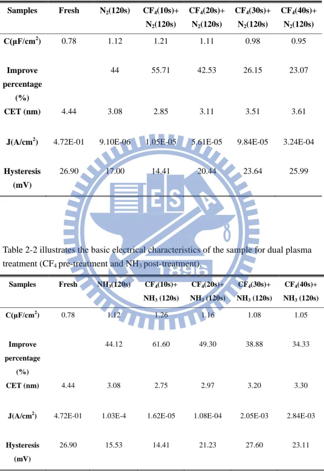
Table 2-1 illustrates the basic electrical characteristics of the sample for dual plasma
treatment (CF4 pre-treatment and N2 post-treatment). 42
Table 2-2 illustrates the basic electrical characteristics of the sample for dual plasma treatment (CF4 pre-treatment and NH3 post-treatment). 42 Table 2-3 Schottky Barrier Height Extracted for The Samples with No Treatment,
Single Plasma Treatment, and Dual Plasma Treatment. 43
Table 2-4 F-P Trapping Level Extracted for The Samples with No Treatment, Single
Plasma Treatment, and Dual Plasma Treatment. 43
Table 2-5 F-N Barrier Height Extracted for The Samples with No Treatment, Single
Plasma Treatment, and Dual Plasma Treatment 43
Chapter 3
Table 3-1 illustrates the basic electrical characteristics of the HfAlOx sample for dual plasma treatment (CF4 pre-treatment and N2 post-treatment). 104 Table 3-2 illustrates the basic electrical characteristics of the HfAlOx sample for dual plasma treatment (CF4 pre-treatment and NH3 post-treatment). 104 Table 3-3 Schottky Barrier Height Extracted for The HfAlOx Samples with No Treatment, Single Plasma Treatment, and Dual Plasma Treatment. 105 Table 3-4 F-P Trapping Level Extracted for The HfAlOx Samples with No Treatment,
Single Plasma Treatment, and Dual Plasma Treatment. 105
Table 3-5 F-N Barrier Height Extracted for The HfAlOx Samples with No Treatment,
xi
Chapter 4
Table 4-1 Device parameters for HfO2 LTPS-TFTs with and without dual plasma
treatment. 139
Table 4-2 Electrical parameters and corresponding possible degradation causes for
HfO2 LTPS-TFTs under HCS. 139
Table 4-3 Electrical parameters degradation under Hot Carrier Stress (HCS) 1000s
with VGS-Vth=5V and drain bias 5V 140
Table 4-4 Electrical parameters degradation under Hot Carrier Stress (HCS) 1000s
with VGS-Vth=5V and drain bias 10V 140
Table 4-5 Electrical parameters degradation under Hot Carrier Stress (HCS) 1000s
xii
Figure Captions
Chapter 1
Fig. 1-1 International Technology Roadmap for Semiconductors (ITRS). Predictions of the gate oxide (SiO2) thickness for future technology generations, which
were defined by the critical device size. 16
Fig. 1-2 The direct tunneling gate current v.s. gate voltage with different gate oxide
thickness. 16
Fig. 1-3 Schematic of direct tunneling through a SiO2 and the thicker high-k gate
dielectric layer. 17
Fig. 1-4 Power consumption and gate leakage current density for a chip which has a 15 Å thick SiO2 gate dielectric compared to the potential reduction in leakage current by an alternate gate dielectric exhibiting the same EOT. Total gate
area of 0.1 cm2. 17
Fig. 1-5 Dielectric constant versus band gap for candidate high-κ materials. 18 Fig. 1-6 Three types of M (metal)-Si-O phase diagrams at fixed temperature and pressure: (a) SiO2 dominant, (b) No phase dominant, and (c) Metal oxide
dominant. 18
Fig. 1-7 The relation of band offsets with carrier injection of electrons and holes in
gate oxide band states. 19
Fig. 1-8 The band alignments of typical high-k gate dielectrics. 19 Fig. 1-9 Energy band diagram of Schottky emission current conduction mechanism. 20 Fig. 1-10 Energy band diagram of Frenkel-Poole emission current conduction
mechanism. 20
Fig. 1-11 Energy band diagram of Fowler-Nordheim tunneling current conduction 21
Fig. 1-12 Schematic illustration of N incorporation effects : 21
Fig. 1-13 Inner-interface trapping model of HfO2 for sweeping voltage from (a)
accumulation to (b) inversion. 22
Fig. 1-14 Inner-interface trapping model of HfO2 after CF4 plasma treatment for
xiii
Chapter 2
Fig. 2-1 Schematic of key process flow of two experiments in this study (a) single nitrogen post-treatment and (b) dual plasma treatment (CF4 pre-treatment
and nitrogen post-treatment). 44
Fig. 2-2 The C-V and I-V characteristics of the HfO2 thin films with N2 post-treatment
for different process durations. 45
Fig. 2-3 The C-V and I-V characteristics of the HfO2 thin films with NH3
post-treatment for different process durations. 46
Fig. 2-4 The C-V characteristics of the HfO2 thin films treated in CF4 plasma for
different process durations and N2 plasma for 120 sec. 47
Fig. 2-5 The J-V characteristics of the HfO2 thin films treated in CF4 plasma for
different process durations and N2 plasma for 120 sec. 47
Fig. 2-6 The C-V characteristics of the HfO2 thin films treated in CF4 plasma for different process durations and NH3 plasma for 120 sec. 48 Fig. 2-7 The J-V characteristics of the HfO2 thin films treated in CF4 plasma for different process durations and NH3 plasma for 120 sec. 48 Fig. 2-8 The hysteresis characteristics of the HfO2 thin films treated in CF4 plasma for
different process durations and N2 plasma for 120 sec. 49
Fig. 2-9 The hysteresis characteristics of the HfO2 thin films treated in CF4 plasma for different process durations and NH3 plasma for 120 sec. 50 Fig. 2-10 Frequency dependence of C-V curve for the Al/Ti/HfO2/Si MIS capacitors
for fresh sample. 51
Fig. 2-11 frequency dependence of C-V curve for the Al/Ti/HfO2/Si MIS capacitors
treated in N2 120 sec. 51
Fig. 2-12 Frequency dependence of C-V curve for the Al/Ti/HfO2/Si MIS capacitors
treated in CF4 10 sec + N2 120 sec. 52
Fig. 2-13 Frequency dependence of C-V curve for the Al/Ti/HfO2/Si MIS capacitors
treated in CF4 20 sec + N2 120 sec. 52
Fig. 2-14 Frequency dependence of C-V curve for the Al/Ti/HfO2/Si MIS capacitors
treated in CF4 30 sec + N2 120 sec. 53
Fig. 2-15 Frequency dependence of C-V curve for the Al/Ti/HfO2/Si MIS capacitors
for treated in CF4 40 sec + N2 120 sec. 53
Fig. 2-16 Frequency dependence of C-V curve for the Al/Ti/HfO2/Si MIS capacitors
treated in NH3 120 sec. 54
Fig. 2-17 Frequency dependence of C-V curve for the Al/Ti/HfO2/Si MIS capacitors
xiv
Fig. 2-18 Frequency dependence of C-V curve for the Al/Ti/HfO2/Si MIS capacitors
treated in CF4 20 sec + NH3 120 sec. 55
Fig. 2-19 Frequency dependence of C-V curve for the Al/Ti/HfO2/Si MIS capacitors
treated in CF4 30 sec + NH3 120 sec. 55
Fig. 2-20 Frequency dependence of C-V curve for the Al/Ti/HfO2/Si MIS capacitors
treated in CF4 40 sec + NH3 120 sec. 56
Fig. 2-21 C-V curves of Al/Ti/HfO2/Si MIS capacitors for Fresh sample before and
after CVS condition. The stress voltage is -3 V. 56
Fig. 2-22 C-V curves of Al/Ti/HfO2/Si MIS capacitors treated in N2 120 sec before
and after CVS condition. The stress voltage is -3 V. 57
Fig. 2-23 C-V curves of Al/Ti/HfO2/Si MIS capacitors treated in CF4 10 sec + N2 120 sec before and after CVS condition. The stress voltage is -3 V. 57 Fig. 2-24 C-V curves of Al/Ti/HfO2/Si MIS capacitors treated in CF4 20 sec + N2 120 sec before and after CVS condition. The stress voltage is -3 V. 58 Fig. 2-25 C-V curves of Al/Ti/HfO2/Si MIS capacitors treated in NH3 120 sec before
and after CVS condition. The stress voltage is -3 V. 58
Fig. 2-26 C-V curves of Al/Ti/HfO2/Si MIS capacitors treated in CF4 10 sec + NH3 120 sec before and after CVS condition. The stress voltage is -3 V. 59 Fig. 2-27 C-V curves of Al/Ti/HfO2/Si MIS capacitors treated in CF4 20 sec + NH3
120 sec before and after CVS condition. The stress voltage is -3 V. 59 Fig. 2-28 Schematic of the band diagram of HfO2 gate stake structure under constant
negative voltage stress. 60
Fig. 2-29 The J-E curves plots for the sample without treatment at different
temperatures from 298 K to 398 K. 60
Fig. 2-30 The J-E curves plots for the sample treated in N2 120 sec at different
temperatures from 298 K to 398 K. 61
Fig. 2-31 The J-E curves plots for the sample treated in CF4 10 sec + N2 120 sec at
different temperatures from 298 K to 398 K. 61
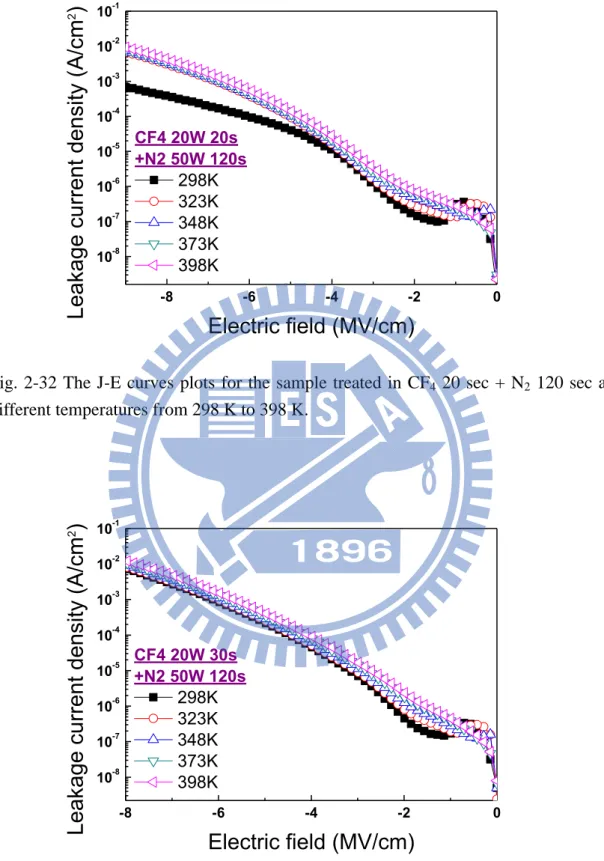
Fig. 2-32 The J-E curves plots for the sample treated in CF4 20 sec + N2 120 sec at
different temperatures from 298 K to 398 K. 62
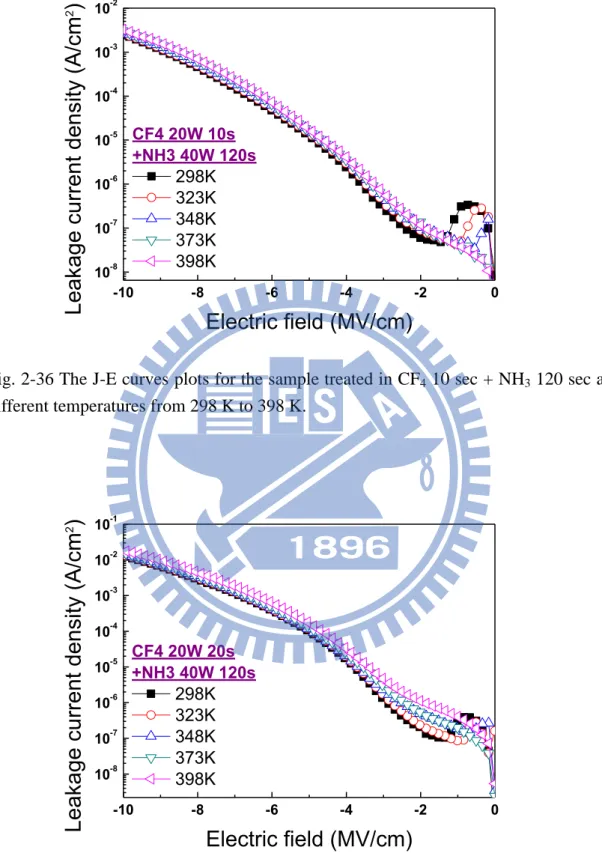
Fig. 2-33 The J-E curves plots for the sample treated in CF4 30 sec + N2 120 sec at
different temperatures from 298 K to 398 K. 62
Fig. 2-34 The J-E curves plots for the sample treated in CF4 40 sec + N2 120 sec at
different temperatures from 298 K to 398 K. 63
Fig. 2-35 The J-E curves plots for the sample treated in NH3 120 sec at different
temperatures from 298 K to 398 K. 63
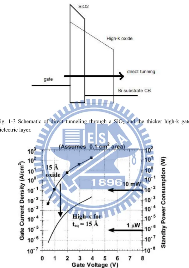
Fig. 2-36 The J-E curves plots for the sample treated in CF4 10 sec + NH3 120 sec at
xv
Fig. 2-37 The J-E curves plots for the sample treated in CF4 20 sec + NH3 120 sec at
different temperatures from 298 K to 398 K. 64
Fig. 2-38 The J-E curves plots for the sample treated in CF4 30 sec + NH3 120 sec at
different temperatures from 298 K to 398 K. 65
Fig. 2-39 The J-E curves plots for the sample treated in CF4 40 sec + NH3 120 sec at
different temperatures from 298 K to 398 K. 65
Fig. 2-40 Schottky emission plots, ln(J/T2) versus E1/2, for the HfO2 thin film with no treatment at different temperatures (348K, 373K, and 398K). 66 Fig. 2-41 Schottky emission plots, ln(J/T2) versus E1/2, for the HfO2 thin film with N2
120 sec at different temperatures (348K, 373K, and 398K). 66 Fig. 2-42 Schottky emission plots, ln(J/T2) versus E1/2, for the HfO2 thin film with CF4
10 sec + N2 120 sec at different temperatures (348K, 373K, and 398K). 67 Fig. 2-43 Schottky emission plots, ln(J/T2) versus E1/2, for the HfO2 thin film with CF4
20 sec + N2 120 sec at different temperatures (348K, 373K, and 398K). 67 Fig. 2-44 Schottky emission plots, ln(J/T2) versus E1/2, for the HfO2 thin film with CF4
30 sec + N2 120 sec at different temperatures (348K, 373K, and 398K). 68 Fig. 2-45 Schottky emission plots, ln(J/T2) versus E1/2, for the HfO2 thin film with CF4
40 sec + N2 120 sec at different temperatures (348K, 373K, and 398K). 68 Fig. 2-46 Schottky emission plots, ln(J/T2) versus E1/2, for the HfO2 thin film with NH3 120 sec at different temperatures (348K, 373K, and 398K). 69 Fig. 2-47 Schottky emission plots, ln(J/T2) versus E1/2, for the HfO2 thin film with CF4
10 sec + NH3 120 sec at different temperatures (348K, 373K, and 398K). 69 Fig. 2-48 Schottky emission plots, ln(J/T2) versus E1/2, for the HfO2 thin film with CF4
20 sec + NH3 120 sec at different temperatures (348K, 373K, and 398K). 70 Fig. 2-49 Schottky emission plots, ln(J/T2) versus E1/2, for the HfO2 thin film with CF4
30 sec + NH3 120 sec at different temperatures (348K, 373K, and 398K). 70 Fig. 2-50 Schottky emission plots, ln(J/T2) versus E1/2, for the HfO2 thin film with CF4
40 sec + NH3 120 sec at different temperatures (348K, 373K, and 398K). 71 Fig. 2-51 The band diagram of Al/Ti/HfO2/Si MIS capacitors for the Schottky emission under gate injection. qφB is the Schottky barrier height. 71 Fig. 2-52 Frenkel-Poole emission plots, ln(J/E) versus E1/2, for the HfO2 thin film with
no treatment at different temperatures (298 - 398 K). 72
Fig. 2-53 Frenkel-Poole emission plots, ln(J/E) versus E1/2, for the HfO2 thin film with
N2 120 sec at different temperatures (298 - 398 K). 72
Fig. 2-54 Frenkel-Poole emission plots, ln(J/E) versus E1/2, for the HfO2 thin film with CF4 10 sec + N2 120 sec at different temperatures (298 - 398 K). 73 Fig. 2-55 Frenkel-Poole emission plots, ln(J/E) versus E1/2, for the HfO2 thin film with CF4 20 sec + N2 120 sec at different temperatures (298 - 398 K). 73
xvi
Fig. 2-56 Frenkel-Poole emission plots, ln(J/E) versus E1/2, for the HfO2 thin film with CF4 30 sec + N2 120 sec at different temperatures (298 - 398 K). 74 Fig. 2-57 Frenkel-Poole emission plots, ln(J/E) versus E1/2, for the HfO2 thin film with CF4 40 sec + N2 120 sec at different temperatures (298 - 398 K). 74 Fig. 2-58 Frenkel-Poole emission plots, ln(J/E) versus E1/2, for the HfO2 thin film with
NH3 120 sec at different temperatures (298 - 398 K). 75
Fig. 2-59 Frenkel-Poole emission plots, ln(J/E) versus E1/2, for the HfO2 thin film with CF4 10 sec + NH3 120 sec at different temperatures (298 - 398 K). 75 Fig. 2-60 Frenkel-Poole emission plots, ln(J/E) versus E1/2, for the HfO2 thin film with CF4 20 sec + NH3 120 sec at different temperatures (298 - 398 K). 76 Fig. 2-61 Frenkel-Poole emission plots, ln(J/E) versus E1/2, for the HfO2 thin film with CF4 30 sec + NH3 120 sec at different temperatures (298 - 398 K). 76 Fig. 2-62 Frenkel-Poole emission plots, ln(J/E) versus E1/2, for the HfO2 thin film with CF4 40 sec + NH3 120 sec at different temperatures (298 - 398 K). 77 Fig. 2-63 Plots of ln(JFP/E) versus 1/T at various electric fields for Fresh sample. qφt
is the trap energy level in HfO2. 77
Fig. 2-64 Plots of ln(JFP/E) versus 1/T at various electric fields for the sample treated
in N2 120 sec. qφt is the trap energy level in HfO2. 78
Fig. 2-65 Plots of ln(JFP/E) versus 1/T at various electric fields for the sample treated in CF4 10 sec + N2 120 sec. qφt is the trap energy level in HfO2. 78 Fig. 2-66 Plots of ln(JFP/E) versus 1/T at various electric fields for the sample treated in CF4 20 sec + N2 120 sec. qφt is the trap energy level in HfO2. 79 Fig. 2-67 Plots of ln(JFP/E) versus 1/T at various electric fields for the sample treated in CF4 30 sec + N2 120 sec. qφt is the trap energy level in HfO2. 79 Fig. 2-68 Plots of ln(JFP/E) versus 1/T at various electric fields for the sample treated in CF4 40 sec + N2 120 sec. qφt is the trap energy level in HfO2. 80 Fig. 2-69 Plots of ln(JFP/E) versus 1/T at various electric fields for the sample treated in NH3 120 sec. qφt is the trap energy level in HfO2. 80 Fig. 2-70 Plots of ln(JFP/E) versus 1/T at various electric fields for the sample treated in CF4 10 sec + NH3 120 sec. qφt is the trap energy level in HfO2. 81 Fig. 2-71 Plots of ln(JFP/E) versus 1/T at various electric fields for the sample treated in CF4 20 sec + NH3 120 sec. qφt is the trap energy level in HfO2. 81 Fig. 2-72 Plots of ln(JFP/E) versus 1/T at various electric fields for the sample treated in CF4 30 sec + NH3 120 sec. qφt is the trap energy level in HfO2. 82 Fig. 2-73 Plots of ln(JFP/E) versus 1/T at various electric fields for the sample treated in CF4 40 sec + NH3 120 sec. qφt is the trap energy level in HfO2. 82 Fig. 2-74 Trapping energy levels extracted from F-P fitting for the samples with dual plasma treatment (a) CF4 plasma and N2 plasma (b) CF4 plasma and NH3
xvii
plasma. 83
Fig. 2-75 Schematic of the band diagram of Al/Ti/HfO2/Si MIS capacitors before and after dual plasma treatment for the Frenkel Poole emission under gate
injection. 84
Fig. 2-76 F-N tunneling characteristic, ln(J/E2) vs. 1/E, for the samples with dual plasma treatment (a) CF4 plasma and N2 plasma (b) CF4 plasma and NH3
plasma 85
Fig. 2-77 The band diagram of Al/Ti/HfO2/Si MIS capacitors for Fowler-Nordheim tunneling under gate injection. qφt is the FN potential barrier height. 86 Fig. 2-78 The summary of the three current conduction mechanisms in different
ranges of applied gate voltage. 86
Chapter 3
Fig. 3-1 Key process flows of two experiments in this work for (a) single nitrogen post-treatment and (b) dual plasma treatment (CF4 pre-treatment and
nitrogenpost-treatment) 106
Fig. 3-2 The C-V characteristics of the HfAlOx thin films with N2 post-treatment for
different process durations. 107
Fig. 3-3 The I-V characteristics of the HfAlOx thin films with N2 post-treatment for
different process durations. 107
Fig. 3-4 The C-V characteristics of the HfAlOx thin films with NH3 post-treatment for
different process durations. 108
Fig. 3-5 The I-V characteristics of the HfAlOx thin films with NH3 post-treatment for
different process durations. 108
Fig. 3-6 The C-V characteristics of the HfAlOx thin films treated in CF4 plasma for
different process durations and N2 plasma for 90 sec. 109
Fig. 3-7 The J-V characteristics of the HfAlOx thin films treated in CF4 plasma for
different process durations and N2 plasma for 90 sec. 109
Fig. 3-8 The C-V characteristics of the HfAlOx thin films treated in CF4 plasma for different process durations and NH3 plasma for 90 sec. 110 Fig. 3-9 The J-V characteristics of the HfAlOx thin films treated in CF4 plasma for different process durations and NH3 plasma for 90 sec. 110 Fig. 3-10 The hysteresis characteristics of the HfAlOx thin films treated in CF4 plasma for different process durations and N2 plasma for 90 sec. 111
xviii
Fig. 3-11 The hysteresis characteristics of the HfAlOx thin films treated in CF4 plasma for different process durations and NH3 plasma for 90 sec. 112 Fig. 3-12 Breakdown behavior of HfAlOx MIS capacitor treated in (a) CF4 and N2
plasma treatment, and (b) CF4 and N2 plasma treatment. 113 Fig. 3-13 The Weibull plot of the breakdown voltage HfAlOx MIS capacitor treated in (a) CF4 and N2 plasma treatment, and (b) CF4 and N2 plasma treatment. 114 Fig. 3-14 C-V frequency dispersion characteristics of the HfAlOx thin films treated in CF4 plasma for different process durations and N2 plasma for 90 sec. 115 Fig. 3-15 C-V frequency dispersion characteristics of the HfAlOx thin films treated in CF4 plasma for different process durations and NH3 plasma for 90 sec. 115 Fig. 3-16 The C-V curves before and after CVS characteristics of the HfAlOx thin films treated in CF4 plasma for different process durations and N2 plasma
for 90 sec. 116
Fig. 3-17 The C-V curves before and after CVS characteristics of the HfAlOx thin films treated in CF4 plasma for different process durations and NH3 plasma
for 90 sec. 116
Fig. 3-18 Schottky emission plots, ln(J/T2) versus E1/2, for the HfAlOx thin film with (a) CF4 plasma + N2 plasma (b) CF4 plasma + NH3 plasma at different
temperatures 117
Fig. 3-19 Trapping energy levels extracted from F-P fitting for the HfAlOx samples with dual plasma treatment (a) CF4 plasma and N2 plasma (b) CF4 plasma
and NH3 plasma. 118
Fig. 3-20 F-N tunneling characteristic, ln(J/E2) vs. 1/E, for the HfAlOx samples with dual plasma treatment (a) CF4 plasma and N2 plasma (b) CF4 plasma and
NH3 plasma 119
Chapter 4
Fig. 4-1 Schematic of process flow of high-κ HfO2 gate dielectric LTPS TFT structure
with dual plasma treatment. 142
Fig. 4-2 The transfer characteristics IDS-VGS of the HfO2 LTPS-TFTs with and without
dual plasma treatment at Vd=0.1V and Vd=1V. 143
Fig. 4-3 The C-V curve of the HfO2 MIS capacitor with and without dual plasma
treatment. 143
xix
measured at Vd=0.1V. 144
Fig. 4-5 The plots of the ln[ID/(VG-VFB)2] versus 1/(VG-VFB)2 curves at VD=1V. 144 Fig. 4-6 Active energy (Ea) versus gate voltage of HfO2 LTPS TFTs with and without
dual plasma treatment. 145
Fig. 4-7 The output characteristics (ID-VG) of HfO2 LTPS TFTs with and without dual
plasma treatment. 145
Fig. 4-8 SID/Ids2 of the HfO2 LTPS TFTs with and without dual plasma treatment at
VDS=0.1V and VG-VT=1V. 146
Fig. 4-9 The ID-VG characteristic of HfO2 LTPS-TFT with dual plasma treatment before and after negative bias stress (NBS) and positive bias stress (PBS) with VG = -5V, -3.86V, 0V, 6.14V and VD = VS = 0V for 1500 s at T =
25°C. 146
Fig. 4-10 The IG-VG characteristic of HfO2 LTPS-TFT with dual plasma treatment before and after negative bias stress (NBS) and positive bias stress (PBS) with VG = -5V, -3.86V, 0V, 6.14V and VD = VS = 0V for 1500 s at T =
25°C. 147
Fig. 4-11 The band diagram of the oxide after PBS and NBS. 147
Fig. 4-12 Subthreshold swing S.S. and the transconductance Gm of the HfO2 LTPS-TFT with dual plasma treatment before and after NBS and PBS. 148 Fig. 4-13 The transconductance (Gm) of the HfO2 LTPS-TFT with and without dual
plasma treatment before and after NBS and PBS. 148
Fig. 4-14 The subthreshold swing (S.S.) of the HfO2 LTPS-TFT with and without
dual plasma treatment before and after NBS and PBS. 149
Fig. 4-15 The ID versus VG curves with stress time of n-type HfO2 LTPS-TFT with dual plasma treatment under PBI stress with VG-VTH ~ 5V at T=25oC. 149 Fig. 4-16 The ID versus VG curves with stress time of n-type HfO2 LTPS-TFT without plasma treatment under PBI stress with VG-VTH ~ 5V at T=25oC. 150 Fig. 4-17 Time evolutions of ΔVth for n-type HfO2 LTPS-TFT with and without
plasma treatment under PBI stress at VG-VTH ~ 5V. 150
Fig. 4-18 Band diagrams of the Si substrate showing the occupation of interface states and different charge polarities when operating at inversion. (a) P-type substrate with positive interface charge at flatband and negative interface trap charge at inversion. (b) N-type substrate with negative interface charge at flatband and positive interface trap charge at inversion. 151 Fig. 4-19 Time evolutions of ΔNit for n-type HfO2 LTPS-TFT with and without
plasma treatment under PBI stress at VG-VTH ~ 5V. 152
Fig. 4-20 The variations percentage of the drive current (ΔIDS) under PBI stress. 152 Fig. 4-21 The ID versus VG curves with stress time of n-type HfO2 LTPS-TFT with
xx
plasma treatment under PBTI stress with VG-VTH ~ 5V at T=100oC. 153 Fig. 4-22 The ID versus VG curves with stress time of n-type HfO2 LTPS-TFT without dual plasma treatment under PBTI stress with VG-VTH ~ 5V at T=100oC.
153 Fig. 4-23 Time evolutions of ΔVth for n-type HfO2 LTPS-TFT with and without plasma treatment under PBTI stress with VG-VTH ~ 5V at T=100oC 154 Fig. 4-24 Time evolutions of ΔNit for n-type HfO2 LTPS-TFT with and without plasma treatment under PBTI stress with VG-VTH ~ 5V at T=100oC 154 Fig. 4-25 The gate leakage current with stress time for n-type HfO2 LTPS-TFT with dual plasma treatment under PBTI stress with VG-VTH ~ 5V at T=100oC.
155 Fig. 4-26 The gate leakage current with stress time for n-type HfO2 LTPS-TFT without plasma treatment under PBTI stress with VG-VTH ~ 5V at T=100oC.
155 Fig. 4-27 ID-VG curves of the dual plasma sample stressed in different drain voltages
(5-20V) with VG-VT=5V for 1000 sec. 156
Fig. 4-28 ID-VG curves of the control sample stressed in different drain voltages
(5-20V) with VG-VT=5V for 1000 sec. 156
Fig. 4-29 The output characteristics of the dual plasma sample for (a) normal mode and (b) reverse mode after HCS 1000s with VGS-Vth=5V and drain bias 15V. 157 Fig. 4-30 The Hf 4f ESCA spectra of the HfO2 LTPS-TFT without plasma treatment.
158 Fig. 4-31 The Hf 4f ESCA spectra of the HfO2 LTPS-TFT with dual plasma treatment. 158
1
Chapter 1
Introduction
1.1 Background
The complementary metal oxide semiconductor (CMOS) field effect transistor (FET) plays the important role in modern electronic industry. In order to have greater integrated circuit functionality, lower power consumption, higher performance, and lower cost, the demand of the industry requires the higher density of transistors on the wafer, which means the feature size of the transistor need to become smaller. In 1965, Gordon E. Moore proposed the “Moore’s law” to predict the number of devices increases doubled per wafer every year [1], and he revised the projection of law from every year to every two year in 1975 [2].
The drive current associated with metal oxide semiconductor (MOS) field effect transistor (FET) could be written as
D D T G inv D V V V V C L W I 2 , (1) where W and L are the width and channel length of the transistor channel respectively, μ is the channel carrier mobility, Cinv is the capacitance density associated with the gate dielectric when the transistor is inverted, VG is the voltage applied on transistor’s gate, VT is the threshold voltage, VD is the applied voltage on drain terminal of the transistor. At first, the drain current (ID)increases linearly with the drain voltage (VD)
2
and finally saturates to maximum at VD=VG-VT, leading to
2 2 , T G inv sat D V V C L W I . (2)According to eq. (2), there are some ways to improve the performance, including increase the term (VG-VT), reduce the channel length (L), and increase the channel width (W) and the gate dielectric capacitance (Cinv).
In terms of the increase (VG-VT), it is limited in a range because of reliability and room temperature operation constraints [3]. Too large VG will create undesirable high electric field across the gate dielectric, inducing the high leakage current, high power consumption, and reliability problems. Moreover, VT could not easily be reduced below 200 mV. Because kT is approximate 25mV at room temperature, the specific temperature would adversely affect the VT value, causing statistical fluctuation in thermal energy.
Even through the shrinkage of the channel length (L) could achieve density, speed, and power improvements, the scaling cannot go on forever. The continue shortening of the channel length will not only increase the fabrication complexity but also cause the undesirable physical phenomena, which called short-channel effect [4]. There are five different effects of short channel in MOSFET, such as drain-induced barrier lowering (DIBL) or punch-through, velocity saturation, channel length modulation, source-drain series resistance, and MOSFET breakdown [5]-[8].
An FET is a capacitance-operated device; in other words, the source-drain current of the FET depends on the gate capacitance Cox. The Cox which ignored depletion effects and quantum mechanism for silicon substrate [9] could be written
t A Cox0
3
where ε0 is the permittivity of free space (8.85×10⁻¹⁴ F/cm), κ is the dielectric constant (relative permittivity) of the material, t is thickness of the gate oxide dielectric and A is the area of the capacitor. Based on eq. (3), the gate capacitance could be increased by decreasing the thickness of the gate oxide. However, the aggressive shrinking of the gate length and gate dielectric thickness accompanies excessive leakage current and reliability problems. Fig. 1-1 shows the prediction of the gate oxide (SiO2) thickness for feature technology node. According to the prediction, the gate oxide would be so thin that would be 1.3 nm in 2012, which only consists of three atomic layers [10]. Fig. 1-2 shows the gate leakage current with different oxide thickness. The direct tunneling leakage current from the quantized inversion layer increase exponentially with decreasing oxide thickness [11]. The leakage current becomes problematic when oxide thickness below 20 Ǻ. To solve these problems, a major solution is to replace the traditional SiO2 or SiON by other higher dielectric constant material.
1.2 High-κ gate dielectric
1.2.1 Advantages of high-κ gate dielectric
In terms of the electrical design of the device, it is convenient to define an electrical thickness of the high-κ gate dielectric. According to eq. (3), the capacitance could be expressed in terms of teq (equivalent oxide thickness (EOT)) and 3.9 (dielectric constant of SiO2).
high high eq EOT t t 3.9 . (4)
4
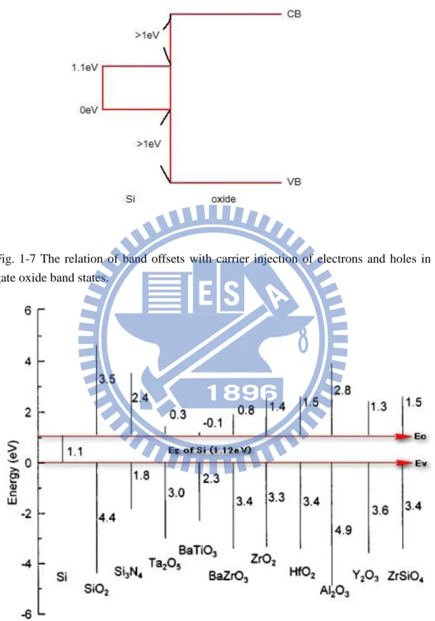
The term teq represents the theoretical thickness of SiO2 that was required to achieve the same capacitance density as the dielectric. Using high dielectric constant material for gate dielectric could have larger physical thickness and maintain smaller equivalent oxide thickness (EOT), as shown in Fig. 1-3. The direct tunneling current would be decreased due to larger physical thickness. Compared to the high performance microprocessor market, transistors with lower (about 10-3 A/cm2) leakage currents would be required for the rapidly growing market of low-power applications. Fig. 1-4 shows the gate current density and the standby power consumption as a function of gate voltage. Compared to 15 Ǻ oxide, the high-κ gate dielectric with same EOT shows the great reduction of the gate leakage and power consumption. As a result, the gate dielectric with higher permittivity than oxide is required for low power device. In short, high-dielectric-constant (high-κ) thin films have been considered as suitable gate dielectric for modern CMOS technology.
1.2.2 Choice of the high-κ gate dielectric
To minimize the direct tunneling current, the ultrathin silicon oxynitride (SiON) is a solution to replace silicon oxide (SiO2) when conventional oxide cannot be scaled down. Several researches focus on applying different methods to optimize the quality of ultrathin oxynitride to substitute conventional oxide since 1990 [12]-[15]. It has been reported that oxynitride has ability to prevent boron diffusion from gate electrode to substrate in pMOSFETs [16, 17], suppress the hot-carrier degradation and enhance electron mobility in nMOSFETs [18, 19], and reduce the equivalent oxide thickness or leakage current [20, 21]. The dielectric permittivity () of oxynitride depends on its content of nitrogen. Unfortunately, the oxynitride only extends the gate dielectric two or three (90-40nm) generations because the value is not higher enough. As a result, high- material becomes a candidate to replace conventional
5
oxide and oxynitride. The principle of choosing the high- material is described as follows [22]:
(a) The κ value must be high enough.
Table 1-1 shows the main high-κ gate dielectric materials with their parameters: ε is the permittivity, Eg is the band gap, CBO is the conduction band offset, and VBO is the valence band offset [23]. Fig. 1-5 depicts the relation between the κ value and the dielectric band gap [24]. It can be seen that the κ value tends to vary inversely with the band gap. The first requirement is the κ value should be over 12. There are numerous dielectrics with extremely large κ value, but with unsuitable low band gap. Furthermore, a very large κ is undesirable in CMOS design due to undesirable fringing fields at the source and drain electrode [25]. Consequently, the dielectric, such as HfO2, ZrO2, and La2O3, with κ value within 25-30 is preferable in CMOS technology.
(b) High-κ dielectric should be thermodynamically stable with Si channel.
There usually have extensive inter-diffusion effects or chemical reactions when direct growing high-κ gate dielectric on silicon substrate, resulting in the properties degradation of the gate dielectric, the underlying silicon, or both [26]. The required property of the dielectrics is that it must not react with Si forming either SiO2 or silicide according to the unbalanced reactions
2 2 Si M SiO MO , (5) 2 2 2Si MSi SiO MO . (6)
This reason is that forming SiO2 layer would increase the EOT and negate the effect of using high-κ gate dielectric, whereas forming silicide (eq. (6)) would short out the
6 field effect.
It could be used a ternary phase diagram with tie lines to represent the stability of a gate dielectric in contact with Si, as shown in Fig. 1-6. Tie lines which connect two compositions represent that they could be with each other in equilibrium [22]. As shown in Fig. 1-6(a) and Fig. 1-6(b), MOx could not directly connect to Si unless via the SiO2, for example Ta2O5 or TiO2. On the other hand, metal oxide dominant type shown in Fig. 1-6(c) has a tie line between MOx and Si, which means that high-κ metal oxides could direct connect to Si, such as ZrO2. In short, it should be focus on metal oxide dominant type for choosing high-κ materials, like ZrO2, HfO2, Al2O3, Y2O3, La2O3, Sc2O3 and some lanthanides such as Pr2O3, Gd2O3 and Lu2O3.
(c) Higher energy band gap and conduction band offset with Si should over 1 eV.
The high-κ material should act as a gate insulator in MOS structure. In that case, it requires that the potential barrier at each band must be over 1 eV so that could inhibit conduction by the Schottky emission of electrons or holes into the oxide band [24], as shown schematically in Fig. 1-7. Fig. 1-8 depicts the calculated conduction band and valence band offsets of various oxide on Si. In general, the conduction band offset is usually smaller than the valence band offset; therefore, the limits of the choice on high-κ material should with band gap over 5 eV. The high-κ material such as ZrO2, HfO2, Al2O3, Y2O3, La2O3 and various lanthanides and their silicates and aluminates could satisfy this criterion.
(d) Interface quality
The oxide is directly contact with Si channel, while the carriers in the channel flow within angstroms of the Si-oxide interface. Therefore, the interface must be the highest electrical quality; in other words, the interface should have less roughness and
7 absence of interface defects.
(e) Defects
Defects in the dielectric are the electronic states in the band gap of the oxide, which are usually generated by oxygen vacancies or impurities. There are some reasons that defects are undesirable and should be greatly reduced. First, charge trapped in the defects states in the oxide band gap and would change with time, resulting in the threshold voltage shift and instability of operation voltage. Second, the trapped charge in the defect would induce carrier scattering within the channel, leading to carrier mobility degradation. Third, defects cause the electrical reliability problems of the devices, such as hysteresis, breakdown, hot-carrier stress (HCS), stress-induced leakage current (SILC), time dependent dielectric breakdown (TDDB), positive bias temperature instability (PBTI), and negative bias temperature instability (NBTI).
1.2.3 Hf-based high-κ gate dielectric
In order to replace conventional SiO2 as a gate dielectric thin film, high-κ materials have been investigated, such as ZrO2 [27-29], HfO2 [30-32], Ta2O5 [33], TiO2 [34-36], Y2O3 [37-39], Al2O3 [40, 41], La2O3 [42]. Ta2O5 and TiO2 have too low conduction band offset with Si, thus the leakage current is sensitive to temperature. Al2O3 has the disadvantage of a rather low κ value, whereas Y2O3 has not only lower κ value than HfO2 but also poor thermal stability due to heavily reactive with Si. La2O3 has a slightly higher κ than HfO2, it is hygroscopic though. Although ZrO2 and HfO2 are both generally believed to be two good materials for high-κ gate dielectric, it was found that ZrO2 was slightly reactive with Si forming the silicide ZrSi2 [22]. For this reason, HfO2 was presently the preferred high-κ gate dielectric over ZrO2.
8
In short, HfO2 is a promising gate dielectric layer because it has high dielectric constant (κ ~ 25), relatively large band gap (Eg ~ 5.7 eV), large conduction band offset with Si (~1.5 eV), and stable contact with Si.
1.3 Current conduction mechanisms
The current conduction mechanisms in Hf-based gate dielectrics should be identified. They are generally attributed to Schottky emission (SE), Frenkel-Poole (F-P) emission, and Fowler-Nordheim (F-N) tunneling. Each current transport mechanisms will be introduced in the following.
1.3.1 Schottky emission (SE)
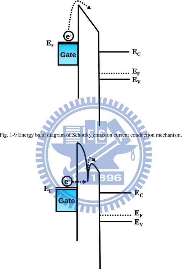
Electrons get enough thermal energy to overcome the potential barrier of the dielectric and transport to the anode, called Schottky emission or thermionic emission. The charge transport process of S.E is shown in Fig. 1-9. The standard Schottky emission could be expressed as
kT qE q T A JSE B r 0 2 * 4 exp , 0 * * 120 m m A ( 2 2 K cm A ), (7)where JSE is the current density, A* is the effective Richardson constant, E is the electric field, T is the absolute temperature, q is the electron charge, qB is the
Schottky barrier height, k is Boltzmann’s constant, ε0 is the permittivity of free space, εr is the dynamic dielectric constant, m* is the electron effective mass, and m0 is the free electron mass.
9
1.3.2 Frenkel-Poole (F-P) emission
When gate under negative bias, electrons will inject from gate into the dielectric layer and will be trapped into shallow trap levels. Thereafter, the electrons transported through the dielectric layer by hopping between these trap levels, leading to leakage current, called Frenkel-Poole (F-P) emission. The charge transport process of F-P is shown in Fig. 1-10. The standard F-P emission could be expressed as
kT qE q E C JFP t t r 0 exp , (8)where JFP is the current density, E is effective electric field, Ct is a constant proportional to the density of bulk oxide traps, qt is the trap energy in oxide, and other parameters are as defined earlier. For the standard Frenkel-Poole emission, a plot of ln(JFP/E) versus E1/2 should be linear. It was found that F-P emission is the dominate conduction mechanism in the region of medium to high electric fields
1.3.3 Fowler-Nordheim (F-N) tunneling
In higher electric field, the Fowler-Nordheim (F-N) tunneling dominated the conduction mechanism. The injection of electrons from the gate entered the conduction band of HfO2 by tunneling through a triangular potential barrier. The charge transport process of F-N is shown in Fig. 1-11. The standard F-N emission could be expressed as
qhE q m AE JFN f 3 2 8 exp 2 3 * 2 , (4)where JFN is the current density, h is the Plunk’s constant, m* is the electron effective mass in oxide, and qf is the potential barrier height.
10
1.4 Motivation
The rapid progress of complementary metal oxide semiconductor (CMOS) integrated circuit technology has met several serious technological challenges over the past few years. According to the prediction of the International Technology Roadmap for Semiconductor (ITRS), the conventional gate dielectric layer will reach its physical limits. Gate dielectric scaling of CMOS will increase the speed and the packing density of modern circuits. However, the aggressive shrinking of the gate length and gate dielectric thickness accompanies excessive leakage current and reliability problems. To solve these problems, a major solution is to replace the traditional SiO2 or SiON by other higher dielectric constant material. Using high dielectric constant material for gate dielectric could have larger physical thickness and maintain smaller equivalent oxide thickness (EOT). As a result, high-dielectric-constant (high-κ) thin films have been considered as suitable gate dielectric for modern CMOS technology. There are various high-κ thin film has been investigated. Among these high-κ materials, HfO2 is considered as the most promising candidate because of high dielectric constant (~25), wide band gap (~5.7 eV), and large band offset with Si conduction band (~1.5 eV). Nevertheless, there are still some issues which need to be considered, such as the reliability and thermal stability of the dielectrics.
1.4.1 Plasma nitridation
It has been reported that nitrogen incorporated into HfO2 gate dielectrics has beneficial effect on performance [43]. As reported in previous study, nitrogen incorporation can suppress crystallization during high temperature treatment, reduce
11
dopant penetration, increase dielectric constant, and reduce leakage current by about 3-4 orders of magnitude [44]. Umezawa et al [45] noted that nitrogen could deactivate the oxygen vacancy related states within HfO2 band gap. The absence of gap states leads to the removal of electron leakage path. Fig. 1-12 illustrates the leakage reduction mechanism of the nitrogen incorporated in HfO2 thin film. When two nitrogen (N) atoms are located nsearby the oxygen vacancy (Vo), two electrons which trapped at the Vo level are transferred to N atoms. As shown in Fig. 1-12(b), the relaxation of Hf atoms causes the elimination of Vo level state, resulting to the removal of electron path in the band gap.
1.4.2 Plasma fluorination
In recently years, the formation of an interfacial layer (IL) at HfO2/Si interface during the growth of dielectric thin film and post processing appears to be a critical issue. Because of low dielectric constant of IL, IL limits the reduction of the effective oxide thickness (EOT). The quality of interfacial layer (IL) becomes more and more important due to gate dielectric scaling. Wang et al noted that the applied electric field would be largely distributed at low-κ layer in high-κ/low-κ stack layer; as a result, the first breakdown happened in the low-κ layer [46].
low high high low E E . (5)Fluorine incorporation also has some improvement on electrical characteristics [47, 48]. Fluorine incorporated into dielectric layer could improve IL quality because of stronger bonding energy of Si-F bonds (5.73 eV) compared to Si-H bonds (3.18eV) [49]. Furthermore, IL at HfO2/Si interface could be suppressed by CF4 pre-treatment [50]. The hysteresis also could be suppressed by fluorine, which could be explained
12
by inner-interface model as shown in Fig. 1-13 and Fig. 1-14.
1.4.2 Dual plasma treatment
There have been many studies using fluorine plasma treatment or nitrogen plasma treatment to improve the performance of the device. In this thesis, we proposed to combine two kinds of plasma treatment (CF4 pre-treatment and nitrogen post-treatment) in order to further improve the electrical characteristics and strength the reliability characteristics of Hf-based MIS capacitor and Low-Temperature Polycrystalline-Silicon (LTPS) Thin-Film Transistor (TFT).
This method that combined CF4 pre-treatment and nitrogen post-treatment is called dual plasma treatment. The purpose of dual plasma treatment is to combine the advantages of two kinds of plasma treatment. We intended to employ CF4 plasma pre-treatment in order to eliminate the low dielectric constant interfacial layer and improved the quality of silicon substrate surface. Moreover, we used the NH3 and N2 plasma post-treatment to reduce oxygen vacancies, increase the permittivity, and increase the crystallization temperature of Hf-based device.
1.5 Organization of the dissertation
In this dissertation, we concentrate our effort to examine the effect of dual plasma treatment (CF4 pre-treatment and nitrogen post-treatment) on the electrical characteristics and the reliability of the Hf-based device. There are five chapters in this dissertation, and the content of each chapter are described as following.
13
including the principle of choosing high-κ materials, and the most candidate high-κ material. Then, we describe the current conduction mechanisms in high-κ dielectric, such as Schottky emission (SE), Frenkel-Poole (F-P) emission, and Fowler-Nordheim (F-N) tunneling. The motivation that new method called dual plasma treatment is launched to combine the advantages of two kinds of plasma treatment (CF4 pre-treatment and nitrogen post-treatment).
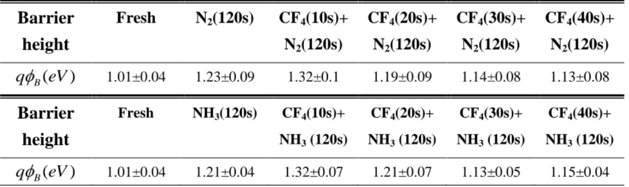
In chapter 2, we propose to combine two kinds of plasma treatment (denoted as dual plasma treatment), CF4 pre-treatment and nitrogen post-treatment, in order to achieve further improvement. We have examined the reliability properties and the current conduction mechanism of HfO2 MIS capacitor structure. First of all, the capacitance-voltage (C-V) characteristics and current-voltage (J-V) characteristics will be briefly described. Second, the frequency dispersion and constant voltage stress (CVS) characteristics of the samples will be analyzed to estimate the improvement. Finally, current conduction mechanisms, such as Schottky emission, Frenkel-Poole (F-P) emission, and Fowler-Nordheim (F-N) tunneling will be discussed. Schottky barrier height, F-P barrier height, and F-N barrier height will be extracted.
In chapter 3, Al/Ti/ HfAlOx/Si MIS capacitor structure would be fabricated. We propose to combine CF4 pre-treatment and N2 post-treatment (denoted as dual plasma treatment) to examine interface quality and reliability properties of HfAlOx MIS capacitor.
In chapter 4, according to chapter 2 and chapter 3, we have demonstrated the dual plasma treatment on MIS capacitor with high-κ gate dielectric. In this chapter, dual plasma treatment (CF4 pre-treatment and N2 post-treatment) will be utilized on LTPS TFTs to reduce defects in poly-Si channel and HfO2 gate dielectric. The
14
electrical improvement would be studied, including the hysteresis and the I-V characteristics. The device parameters, such as Vth, S.S., Gm,μeff,Dit, and Ntrap are extracted to study the improvement effect. Furthermore, the reliability properties and mechanisms of high performance HfO2 gate dielectric LTPS-TFT with dual plasma treatment are investigated, including PBS, NBS, HCS.
Finally, in chapter 5, the summarizations of experimental results in this dissertation and future recommendations are described.
15
Table 1-1 Main high-κ gate dielectric materials with their parameters: ε is the permittivity, Eg is the band gap, CBO is the conduction band offset, and VBO is the valence band offset [23].
16
Fig. 1-1 International Technology Roadmap for Semiconductors (ITRS). Predictions of the gate oxide (SiO2) thickness for future technology generations, which were defined by the critical device size [10].
Fig. 1-2 The direct tunneling gate current vs. gate voltage with different gate oxide thickness [11].
17
Fig. 1-3 Schematic of direct tunneling through a SiO2 and the thicker high-k gate dielectric layer.
Fig. 1-4 Power consumption and gate leakage current density for a chip which has a 15 Å thick SiO2 gate dielectric compared to the potential reduction in leakage current by an alternate gate dielectric exhibiting the same EOT. Total gate area of 0.1 cm2 [3].
18
Fig. 1-5 Dielectric constant versus band gap for candidate high-κ materials [24].
Fig. 1-6 Three types of M (metal)-Si-O phase diagrams at fixed temperature and pressure: (a) SiO2 dominant, (b) No phase dominant, and (c) Metal oxide dominant [26].
19
Fig. 1-7 The relation of band offsets with carrier injection of electrons and holes in gate oxide band states.
20
Fig. 1-9 Energy band diagram of Schottky emission current conduction mechanism.
Fig. 1-10 Energy band diagram of Frenkel-Poole emission current conduction mechanism.
Gate
e
-E
FE
FE
CE
VGate
e
-E
FE
FE
CE
VGate
e
-E
FE
FE
CE
VGate
e
-E
FE
FE
CE
V21
Fig. 1-11 Energy band diagram of Fowler-Nordheim tunneling current conduction mechanism.
Fig. 1-12 Schematic illustration of N incorporation effects :
(a) N-induced atomistic relaxation around Vo: ① Electron transfer from Vo to N atoms,② Outward movement of Hf4+ ions due to the increase in Hf4+- Hf4+ Coulomb repulsion, (b) N-induced elimination of leakage paths: ③ Vo level elevation due to the decrease in attractive Coulomb interaction fromHf4+ ions around Vo,④ removal of leakage paths due to the elimination of a Vo level [45]
Gate e -EF EF EC EV Gate e -EF EF EC EV
22
Fig. 1-13 Inner-interface trapping model of HfO2 for sweeping voltage from (a) accumulation to (b) inversion [48].
Fig. 1-14 Inner-interface trapping model of HfO2 after CF4 plasma treatment for sweeping voltage from (a) accumulation to (b) inversion [48].
23
References
[1]. G. E. Moore,” Cramming more components onto integrated circuits”, Electronics
Mag. vol.38, no.8, pp. 114-117, 1965.
[2]. G. E. Moore, “Progress in Digital Integrated Electronics”, in IEDM Tech. Dig., 1975, pp. 11-13.
[3]. G. D. Wilk, R. M. Wallace, and J. M. Anthony, “High-κ gate dielectrics: Current status and materials properties considerations,” J. Appl. Phys., vol.89, no.10, pp.5243-5275, 2001.
[4]. H. Iwai, “CMOS technology - Year 2010 and beyond,” IEEE journal of
solid-state circuits, vol. 34, pp.357-366, 1999.
[5]. P.R. Troutman,” VLSI limitations from drain-induced barrier lowering”, IEEE J.
Solid State Circuits, vol. 14, no. 2, pp. 383-391, 1979.
[6]. Y. Tau, S. Wind, Y.J. Mii, Y. Lii, D. Moy, K.A. Jenkins, C.L. Chen, P.J. Coane, D. Klaus, J. Bucchignano, M. Rosenfield, M.G.R. Thomson, and M. Polcari,” High performance 0.1 μm CMOS devices with 1.5 V power supply” in IEDM Tech.
Dig., 1993, pp.127-130.
[7]. P. K. Ko, R. S. Muller, and C. Hu,” A unified model for hot-electron currents in MOSFET's“, in IEDM Tech. Dig., pp. 600-603, 1981.
[8]. J.Y.C. Sun, Y. Taur, R.H Dennard, S.P Klepner,” Submicrometer-channel CMOS for low-temperature operation”, IEEE Trans. Electron Devices, vol.34, no.1, pp. 19-27, 1987.
[9]. R. Rios, N. D. Arora, “Determination of ultra-thin gate oxide thicknesses for CMOS structures using quantum effects,” IEDM Tech. Digest, pp. 613-616, 1994.
[10]. M. Schulz, “The end of the road for silicon,” Nature, 399, pp.729-730, 1999. [11]. S.H. Lo, D.A. Buchanan, Y. Tuar, W. Wang, “Quantum-mechanical modeling of
electron tunneling current from the inversion layer of ultra-thin-oxide nMOSFET,” IEEE Electron Devices Lett., 18, pp.209-211, 1997.
[12]. H. Hwang, W. Ting, B. Maiti, D. L. Kwong and J. Lee, “Electrical characteristics of ultrathin oxynitride gate dielectrics prepared by rapid thermal oxidation of
![Fig. 1-5 Dielectric constant versus band gap for candidate high-κ materials [24].](https://thumb-ap.123doks.com/thumbv2/9libinfo/8751881.206101/40.892.163.708.122.992/fig-dielectric-constant-versus-band-candidate-high-materials.webp)
![Fig. 1-14 Inner-interface trapping model of HfO 2 after CF 4 plasma treatment for sweeping voltage from (a) accumulation to (b) inversion [48]](https://thumb-ap.123doks.com/thumbv2/9libinfo/8751881.206101/44.892.148.745.223.894/inner-interface-trapping-treatment-sweeping-voltage-accumulation-inversion.webp)
![Fig. 2-28 Schematic of the band diagram of HfO 2 gate stake structure under constant negative voltage stress [18]](https://thumb-ap.123doks.com/thumbv2/9libinfo/8751881.206101/82.892.147.738.123.1057/schematic-diagram-stake-structure-constant-negative-voltage-stress.webp)