高功率碳化矽金氧半場效電晶體之元件結構與應用之探討
72
0
0
全文
(2) 高功率碳化矽金氧半場效電晶體之元件結構與應用之探討. Investigation of Device structure and Application of SiC Power MOSFET. 學生:楊志潘. Student:Chih-Pan Yang. 指導教授:張國明 博士. Advisor:Dr. Kow-Ming Chang. 國立交通大學電子工程學系電子研究所碩士班 碩士論文. A Thesis Submitted to Institute of Electronics College of Electrical Engineering and Computer Science National Chiao Tung University In Partial Fulfillment of the Requirements for the Degree of Master of Science In Electronics Engineering June 2004 Hsinchu, Taiwan, Republic of China. 中華民國九十三年六月.
(3) 高功率碳化矽金氧半場效電晶體之元件結構與應用之 探討 研究生:楊志潘. 指導教授:張國明 博士. 國立交通大學 電子工程學系 電子研究所碩士班. 摘. 要. 基本上功率電晶體是含有數微米了磊晶矽耐壓區及垂直式的元件結構,在傳 統的雙擴散金氧半功率電晶體,由於在平面通道元件密度及導通阻抗有其極限, 未達高元件密度與低阻抗的要求,往往限制了傳統雙擴散功率的電晶體的表現。 溝槽式閘極高功率金氧半場效電晶體雖有助於改善導通阻抗以增進元件密度,然 在溝槽底部卻需要考慮尖端電場的問題,限制了最大操作電壓。在此嘗試提出一 個高功率碳化矽增強型電晶體結構將有助於改善傳統功率元件的缺點。. 由於以矽為基底的功率電晶體在操作電壓及導通電阻的受限,因碳化矽本身 優越的物質特性,碳化矽功率電晶體逐漸為人所用,本篇論文首先強調碳化矽在 高功率元件元件應用的優勢,引用正確的模型與參數的修正。以期能對不同結構 下的高功率元件所比較的結果做一精確的分析,藉著討論傳統溝槽式及雙擴散式 功率電晶體所面臨的閘極氧化層崩潰及夾止效應,提出一個新式的改良結構,並 以 MEDICI 模擬軟體討論參數的最佳化,並與傳統結構的電晶體做比較,證明其 優越的性質。. i.
(4) Investigation of Device structure and Application of SiC Power MOSFET. Student:Chih-Pan Yang. Advisor:Kow-Ming Chang. Institute of Electronics National Chiao Tung University. ABSTRACT The basic structure of power MOSFET consists of an epitaxial layer for voltage blocking and a drain electrode at the substrate contact. In the conventional double diffused MOSFET, the poor channel resistance and JFET effect limited the DIMOS performance. The trench gate MOSFET, have a much improved on-resistance and packing density because of its vertical channel, however, a high local electric field at the trench corner is of critical importance to the performance of the device. A innovative structure of SiC accumulation-mode MOSFET designed to improve the performance of conventional structure of power MOSFET.. This thesis focused on the design of high voltage MOSFET on SiC power devices. Parameter extraction for 4H-SiC MOS devices is the main focus for this thesis, which includes the mobility parameter extraction. Detailed analysis of the important design parameters of the innovative structure is performed using MEDICI with the parameter been used in calibration process. ii.
(5) 誌謝. 時間荏苒,彷彿才剛踏進來,又到了驪歌高唱的季節,只是,這一次的主角 是自己,在這期間,最感謝我的指導教授,張國明老師對我的在照顧及不厭其煩 的指導,在我的論文及研究上不斷的付出,老師寬厚的待人處事,及研究上觀念 的清晰,對我不論是課業或是看待人事物的方法,皆使我獲益匪淺。. 其次,謝謝陳在泩學長,在模擬軟體及儀器設備的建立上提供我相當多的幫 助,至為感謝。也感謝實驗室的諸多學長、同學及學弟,能一起討論功課以求精 進,在日常生活中一起運動,抒解壓力,提共了大家生活中不少的樂趣,也將是 今後甜美的回憶。. 最後,我要感謝父母對我的栽培,辛苦的默默付出,讓我能專心致志的投入 於課業,完成此碩士學位,也希望能就此學位令我父母感到一點點的光榮!更冀 望以後能帶給父母及家人更多的回報。. iii.
(6) Contents Chinese Abstract ...........................................................................................................i English Abstract ...........................................................................................................ii Acknowledgment ......................................................................................................... iii Contents ......................................................................................................................iv Table Captions ..............................................................................................................vi Figure Captions............................................................................................................vii. Chapter 1 Introduction......................................................................................................................................1. 1.1 Introduction to power devices……………………...………….................................……………………...…1 1.2 Basic structure and operation of power MOSFET………………...…………..................…………2 1.2.1 Basic structure…………..…………………….…………………………….……………………………….…2 1.2.2 Operation of power MOSFET………..……………………………………………………………..…3 1.3 The application of SiC in power devices………….......................………………………….…………...4 1.4Thesis organization……………………………………………........................................................………………..5. Chapter 2 Models and parameters for device simulation...……………........7 2.1 Introduction.....................................................…………………………………………………………………….…...7 2.2 MEDICI description.....................................................................…........................7 2.3 Simulation physical models....................................................……………………………………....................8 2.3.1 The parameter Set for 4H-SiC………………………………………………………………………....9 2.3.2 Carrier mobility in bulk…………………………………………………………………..……………..10 2.3.3 Channel mobility model………………………………………………………………………..……….12 2.4 Impact ionization………………………………………………………………………………………………….15 2.5 Summary………………………………………………………………………………………………………….…..16. Chapter 3 SiC power MOSFET...........................................………………………………..............17 iv.
(7) 3.1 On-resistance.....................………………………………………………………………..........................................17 3.2 The analysis of blocking voltage………………………………………………………………………18 3.3 Material advantages of 4H-SiC for power devices ........................................ 20 3.4 Summary.........................................................................................................................................................................22. Chapter 4 The electrical performance of SiC MOS……………………..………....23. 4.1 Introduction…………………………………………………………………………………………………………..23 4.2 The trench and planar ACCUFET.....…………………………………………..........................................24 4.2.1 The trench ACCUFET.....................................……...............................................................24 4.2.2 The planar ACCUFET.......................................................................................................... 26 4.3 The innovative SiC ACCUFET..………………………………….................……………………..............27 4.4 Analysis and optimization of device parameters....................................................................28 4-5 Summary. 29. Chapter 5 Conclusions.............................................................……….....31. Reference … … … … … … … … … … … … … … … … … … … … … … … … … … … … … … … … … … … … … … 32. v.
(8) Table Captions. Table 1.1 Comparison of Si and SiC material properties Table 2.1 Parameter of low field model for 4H-SiC at 300K Table 2.2 Parameters for 4H-SiC MOSFET mobility models. Table 3.1 Values of doping concentration, electron mobility, drift layer thickness, and specific on-resistance as a function of breakdown voltage for ideal 4H-SiC and Si power MOSFETs at room temperature condition. Table 4.1 Oxide electric field in the trench corner as a functions of trench width, for rectangular and round corner. Table 4.2 The dependence of the oxide electric field at the trench corner of the oxide thickness. Table 4.3 Comparison of ACCUFET structure. vi.
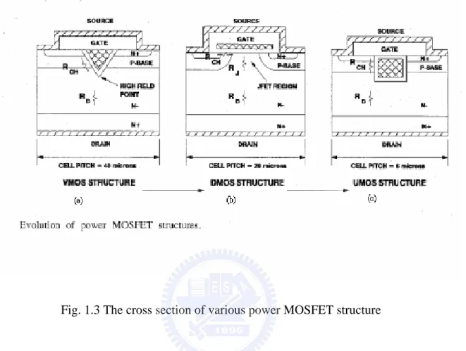
(9) Figure Captions. Fig. 1.1 Applications for power devices in relation to their voltage and current ratings Fig. 1.2 Lateral n-channel MOSFETs cross section Fig. 1.3 The cross section of various power MOSFET structure Fig. 1.4 The operation of power DMOS Fig. 2.1 Low-field electron mobility as a function of doping concentration in 4H-SiC (perpendicular to the c-axis, T = 300 K). Fig. 2.2 Drift velocity of electron in 4H-SiC as functions of the applied field. Fig. 2.3 Mobility between the experimental data and simulation with the parameter values listed in Table 2-2 Fig. 2.4 Temperature dependence of the coefficie nts ap and bp for 4H-SiC Fig. 3.1 A cross section of a power DMOS MOSFETs structure Fig. 4.1 The cross section of trench MOSFET Fig. 4.2 The cross section of accumulation DMOS Fig. 4.3 The relationship between P-base spacing (LP) and Ron Fig. 4.4 The cross section of Innovative SiC ACCUFET Fig. 4.5(a) Effect of peak trench-region concentration on maximum operating voltage. Fig. 4.5(b) Effect of peak trench-region concentration on Ron resistance Fig. 4.5(c) Effect of peak trench-region concentration on BFOM Fig. 4.6(a) Effect of peak trench-region concentration on maximum operating voltage. Fig. 4.6(b) Effect of peak trench-region concentration on Ron resistance. Fig. 4.6(c) Effect of peak trench-region concentration on BFOM. Fig. 4.7(a) Effects of P-base thickness on blocking voltage. Fig. 4.7(b) Effects of P-base thickness on Ron resistance.. vii.
(10) Fig. 4.7(c) Effects of P-base thickness on Ron resistance.. viii.
(11) Chapter 1 Introduction 1-1 Introduction to power devices The development of electronic power systems based on semiconductor devices can be traced to the early 1950s. At that time, the first rectifiers and thyristors are capable of operating at high current and voltage levels. Since that time considerable progress has been made in discrete power semiconductor device technology. The most important development is the creation of a new family of power devices with high-input-impedance metal oxide semiconductor (MOS) gates. The silicon power MOSFET has become the dominant device technology for these applications. These devices greatly reduce the size and complexity of the control circuitry. This has allowed a large reduction in system cost, marking the power electronics attractive for many new applications such as control of home appliances and for automotive electronics as shown in Fig. 1.1[3].. The power MOSFET is a unipolar device. Current conduction occurs through transport of majority carriers in the drift region without the presence of minority carrier injection required for bipolar transistor operation. No delays are observed as a result of storage or recombination of minority carriers in power MOSFETs during turn-off. Their inherent switching speed is orders of magnitude faster than that for bipolar transistors. This feature is particularly attractive in circuits operating at high frequencies where switching power losses are dominant.. Power MOSFETs have also been found to display an excellent safe operating area, that is,. 1.
(12) they can withstand the simultaneous application of high current and voltage (for a short duration) without undergoing destructive failure. These devices also easily paralleled because the forward voltage drop of power MOSFETs increase with increasing temperature. This feature promotes an even current distribution between paralleled devices.. However, for blocking voltages exceeding e.g., 500V state of the art, silicon power MOSFETs cannot compete against bipolar switches because of high resistance of the drift region. A much favorable situation is given for silicon carbide (SiC) power MOSFETs. Silicon carbide is rapidly maturing as a semiconductor material system since the commercial available single crystal substrates. Due to its high breakdown field, high thermal conductivity, and high-temperature operation, SiC is a attractive semiconductor for future power devices.. 1-2 Basic Structure And Operation of Power MOSFET 1-2-1 Basic Structure An understanding of the operation of MOSFETs can best be gleaned by the first considering the lateral N-channel MOSFET shown in Fig. 1.2. Such devices have the drain, gate, and source terminals on the same surface of the silicon wafer. Although this feature makes them well suited for integration, it is not optimum for achieving a high power rating. The vertical channel structure with source and drain on opposite surfaces of the wafer is more suitable for a power device because more area is available for the source region and because the electric field crowding at the gate is reduced.. Three discrete vertical-channel power MOSFET structure have evolved. A cross section 2.
(13) of these structures is provided in Fig. 1.3. The first structure was the vertical channel V-MOS power FET, shown in Fig. 1.3(a) whose name is driven from the V-shaped groove within which the gate is located. Although the V-MOSFET was the first commercial structure, it was replaced by the DMOSFET because of stability problems during manufacturing and a high local electric field at the tip of the V-groove.. The DMOS structure shown in Fig. 1.3(b) is fabricated by using planar diffusion technology with a refractory gate such as polysilicon, as a mask. In these devices, the Pbase region and the N+ source region are diffused through a common window defined by the edge of the polysilicon gate. The name for this device is driven from this double-diffusion process. The P-base region is driven in deeper than the N+ source. The difference in the lateral diffusion between the P-base and N+source regions defines channel region. This has been the most commercially successful structure.. The third power MOSFET structure that has been explored is the U-MOSFETs structure shown in Fig. 1.3(c). The name for this structure is driven from the U-shaped groove formed in the gate region b using reactive ion etching. The U-groove structure has a higher channel density than either the VMOS or DMOS structures which allows significant reduction in the on-resistance of the device.. 1-2-2 Operation of power MOSFETs The operation of the power MOSFET relies upon the formation of a conductive layer at the surface of the semiconductor as shown in Fig. 1.4. In order to carry current from source to drain in the power MOSFET, it is essential to form a conductive path extending between the. 3.
(14) N+ source regions and the N- drift region. This can be accomplished by applying a positive bias to the gate electrode. The gate modulates the conductivity of the channel region by the strong electric field crated normal to the semiconductor surface through the oxide layer. Note that the current flow occurs solely by transport of majority carriers along a resistive path comprising the channel and drift regions. No minority carrier transport is involved for the power MOSFET during current conduction in the on-state. In order to switch the power MOSFET into the off-state, the gate bias voltage must be reduced to zero by externally shorting the gate electrode of the source electrode. When the gate voltage is removed, the electrons are no longer attracted to the channel and the conductive path from drain to source us broken. The power MOSFET then switches rapidly from the on-state to the off-state without any delays arising from minority carrier storage and recombination as experienced in bipolar devices.. Breakdown voltage and on-resistance are two major consideration in designing a power MOSFET. Breakdown voltage can be determined from Id-Vd characteristics of the device. On-resistance is the total series resistance between the source and the drain terminals when the device is turned on. An ideal power MOSFET exhibits high breakdown voltage and low on-resistance simultaneously. Unfortunately, these two requirements are always not met in real design.. 1-3 The Application of SiC in Power Devices Silicon carbide is a wide energy gap semiconductor that possesses a combination of parameters that makes it ideal for various applications in the electronic industry. Its physical properties such as high electric field strength, high saturation drift velocity, and high thermal. 4.
(15) conductivity, has made SiC as the center of a renewed focus of semiconductor material and device research amongst the other wide energy gap semiconductors. Compare with other wide energy gap semiconductor suchⅢ⁄Ⅴ Nitrides, SiC has tremendous advantages because of rapidly maturing technology for making single crystal substrates.. The relatively low breakdown field in Si and the resistance of the drift region that increases rapidly with increasing blocking voltage generally limit the use of Si MOSFET to 500V and below. The advantage of SiC material properties, See Table 1.1, in particular the high breakdown field, makes SiC MOSFETs a very promising candidate for high power switching devices. The specific on-resistance of the SiC power device is expected to be 100~200 times lower than a similarly rated silicon device. Its much lower thermal minority carrier generation implies lower leakage currents and device operation at higher temperatures, arising from self-heating due to power dissipation, is more tolerable. Moreover, the thermal conductivity of SiC is three higher than Si and even higher than cooper at room temperature, also implying a higher efficiency of heat extraction from the device and a further reduction in the requirements for device cooling.. 1-4 Thesis Organization The first part is the introduction which briefly introduces the topic. Chapter 2 begins with the introduction of the two-dimension device simulator, MEDICI, which is used throughout this thesis. It is followed by the important bulk parameter set for 4H-SiC devices. Chapter3 the SiC power device is then proposed and analyzed. We also make the general analysis of 4H-SiC as compared to Si power MOSFET. The fourth part is “result and discussion” which represents the advantages of silicon carbide applied in power devices. 5.
(16) Finally a conclusion of this thesis is given some recommendation of future work are suggested.. 6.
(17) Chapter 2 Models and Parameters for Device Simulation. Numerical device modeling and simulation are essential for analyzing and developing semiconductor devices. They help a design engineering not only gain an increased understanding of the device operation, but also provide the ability to predict electrical characteristics, behavior, and parameter-effects influence of the device. With this knowledge and abilities the designer a better structure, estimate device performance, perform the analysis of worst case, and optimize device parameters to yield an optimize device performance.. 2.1. Introduction Medici is a powerful device simulation program that can be used to simulate the behavior of MOS and bipolar transistors, and other semiconductor devices [2]. It models the two-dimensional distributions of potential and carrier concentrations in a device. The program can be used to predicted electrical characteristics for arbitrary bias conditions. As in any device simulator, any quantitative, or even qualitative, simulation of device relies heavily on applicable device models and their parameter values. A number of physical models are incorporated in MEDICI for accurate simulations. Furthermore MEDICI also supports a variety of semiconductor materials including SiC [13].. 2-2 MEDICI Description The primary function of Medici is to solve the following three partial differential equations [2]. 7.
(18) The Poisson equation. (. ). ε∇ 2 ψ = −q p − n + N +D − N +A − ρ. (1). Continuity equation for electron and hole. ∂n 1 = ∇ • Jn − Un ∂t q. (2). ∂p − 1 = ∇ • Jp − Up ∂t q. (3). Throughout Medici, ψ is always defined as the intrinsic Fermi potential. That is,. ψ=ψ. intrinsic. . ND+ and NA+ are the ionized impurity concentrations and ρ s is a surface charge. density that may be present due to fixed charge in insulating materials or charged interface states .. The numerical algorithms used in MEDICI to solve the fundamental equations are based on the finite element method, which discretized these equations on a simulation grid. This discretization process yields a set of coupled nonlinear algebratic equations which represent a number of grid points, for the unknown potentials and free-carrier concentrations. This set of coupled nonlinear equations in return must be solved a nonlinear iteration method. Two iteration methods, Gummel’s and Newton’s method are available in MEDICI. Regardless which iteration method used, the solutions are carried out over the entire grid until a self-consistent potential and free-carrier concentrations are obtained. Once the potentials and free-carrier concentrations have been calculated at a given bias, it is possible to determine the quasi-Fermi levels and the hole and electron currents ( Jn and Jp ).. 2-3 Simulation Physical Models 8.
(19) 2-3-1 The Parameter Set for 4H-SiC In order to achieve realistic results, it is imperative to use proper models for the 4H-SiC properties. The most important physical models employed in the simulations are for intrinsic concentration, carrier mobility in bulk, transverse and parallel field within the channel region, SRH recombination, Auger recombination and impact ionization. (1) Intrinsic concentration: Accurate models for the carrier concentration in semiconductor devices are a necessity if qualitatively and quantitatively correct simulation results are to be obtained. The intrinsic carrier concentration ni is determined by the fundamental energy gap Eg and the effective density of states NC and NV in the conduction and valence bands. Where, neglecting band gap narrowing, the intrinsic carrier concentration is [2]. n i (T) = NcNvexp(. − Eg 2kT. ). (4). where Eg is the bandgap energy of the semiconductor, that is,. Eg = Ec − E. (5). where NC and NV are defined as ⎛ T ⎞ Nc(T) = NC300 ⎜ ⎟ ⎝ 300 ⎠ ⎛ T ⎞ Nv(T) = NV300 ⎜ ⎟ ⎝ 300 ⎠. 3/2. (6). 3/2. (7). the parameters NC300 and NV300 are user specified and can be modified from their values on the Material statement to fit the 4H-SiC in unipolar devices. 9.
(20) At high doping levels, the carrier-carrier interaction and overlap of the electron wave functions are not negligible. Since no study of bandgap narrowing effects has been performed, these BGN (bandgap narrowing effects) known from Si are taken into account by an effective carrier concentration [13]. n ie (T) = n i (T)exp(. Vg 2kT. (. ). Vg = C g F + F2 + 0.5. (8). ). (9). with ⎛ N + NA ⎞ ⎟⎟ F = ln⎜⎜ D ⎝ N BGN ⎠. (10). In MEDICI [2]. ⎧ N total ⎪ V.BGN ⎡ + n ie (x, y) = n i • exp⎨ ⎢ln N.BGN 2kT ⎣ ⎪⎩. 2 ⎤⎫ ⎛ N total (x, y) ⎞ ⎪ ⎟⎟ + CON.BGN ⎥ ⎬ ⎜⎜ ln ⎥ N.BGN ⎠ ⎝ ⎦ ⎪⎭. (11). The V.BGN, N.BGN, and CON.BGN are constant parameters that can be adjusted from their default values.. 2-3-2 Carrier mobility in bulk By definition, mobility is a measure of average velocity of free carriers in the presence of an impressed electric field. In the presence of an electric field in a semiconductor, the free electrons and holes are accelerated in opposite directions [23]. As the free carriers are transported along the direction of the electric field, their velocity increases until they undergo scattering. In the bulk, the scattering can occur by either interaction with lattice or at ionized 10.
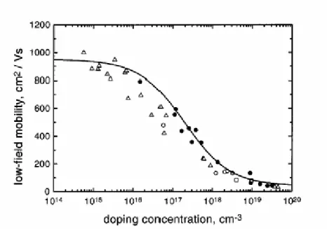
(21) donor and acceptor atoms. In analyzing the influence of the preceding parameters on the mobility, one assumes the electric field strength to be small. The mobility is then defined as the proportionality constant relating the average carrier velocity to the electric field. At high electric field such as those commonly encountered in power devices the velocity is no longer found to increase in proportion to the electric field and in fact attains a saturation value [11]. Since the free-carrier mobility depend strongly on the magnitude of the mobility model on MEDICI consists of low field and high field mobility components. These effects have important implications to current flow in power devices. So the accurate I-V model is strongly based on physical and accurate mobility and velocity saturation models [26].. Low Field Mobility. At low electric fields the electron velocity increases almost linearly with field and the mobility has the constant value µ 0 . The low-field mobility is a function of the doping concentration and the temperature. A widely used empirical expression given by Caughey-Thomas equation for modeling the doping dependence of the low-field mobility has been proposed [25]. µ 0 = µ min +. µ max − µ min ⎛ N 1 + ⎜⎜ ⎝ N ref. ⎞ ⎟⎟ ⎠. (12). α. where N is the total doping concentration, and μ min, μ max ,. Nref ,and α are fitting. parameters. The parameterμmax in (12) represents the mobility of undoped or unintentionally doped samples, where lattice scattering is the main scattering mechanism, whileμmin is the mobility in highly doped material, where impurity scattering is dominant [18]. And Nref is the doping concentration at which the mobility is halfway between μmin and μmax , and α is a measure of how quickly the mobility changes from μmin to μmax .For modeling the. 11.
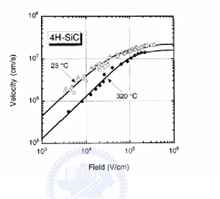
(22) low-field mobility of 4H-SiC at room temperature. Equation (12) has been used. Several sources of experimental data were available for good fitting. Fig. 2.1 shows the experimental low-field mobility fit for 4H-SiC, which the following parameters were determined shown in Table 2.1. High Field Mobility. When strong electric fields are applied, the electron velocity is no longer proportional to the field, and can thus no longer be described by a field independent mobility. An expression frequently used for modeling the field dependence of the mobility in Si is [25] µ0. µ=. ⎛ ⎛µ ×E ⎞ ⎜1 + ⎜ 0 ⎟ ⎜ ⎜⎝ ν sat ⎟⎠ ⎝. β. ⎞ ⎟ ⎟ ⎠. (13). 1 β. where µ 0 is the low field mobility described in (12) ν sat is the saturation velocity, and β is a constant specifying how abruptly the velocity goes into saturation. To obtain the velocity-field characteristics, both sides of (13) have to be multiplied by the electric field. Only little is known about the high-field mobility of SiC. For 4H-SiC the only experimental data on this comes from Khan and Cooper [26], where the drift velocity in epitaxial 4H-SiC (n-doped to about 1017cm-3 ) was measured as a function of the applied electric field. A fit of equation (13) through the experimental high field data by Khan and Cooper is shown in Fig. 2.2, and the µ 0 , ν sat , and β parameter values at 300K are 450 cm2/Vs, 2.2x107cm/s, and 1.2 respectively.. 2-3-3 Channel mobility model 12.
(23) SiC is a viable semiconductor for high-power device applications due to its superior material properties. Although several MOS-based high-voltage devices have been demonstrated, most of them suffer from large on-state resistance due to poor inversion-layer mobility, attributed to a large interface state density at the interface [19]. The use of accumulation-mode MOSFETs was suggested to circumvent the poor inversion-layer mobility problem because a larger accumulation-layer mobility is expected compared to inversion-layer mobility as seen in Si MOS technology [22]. Extracted parametric mobilities and threshold voltage are shown for inversion and accumulation mode MOSFETS on both 4H-SiC and 6H-SiC in Fig. 2.3. Medici also incorporates an empirical model that combines mobility expressions for. semiconductor-insulator interfaces and for bulk silicon. The basic equation is given by Mathiessen’s rule [27]:. ⎡ 1 1 1 ⎤ µs = ⎢ + + ⎥ ⎣ µ ac µ b µ sr ⎦. −1. (14). where µ s is total electron or hole mobility accounting for surface effects. µ ac is the carrier mobility limited by lattice scattering (surface acoustic phonons). µ b is mobility in bulk silicon. µ sr is mobility degraded by surface roughness scattering.. Where µ b is the carrier mobility in bulk of the semiconductor, µ ac is the carrier mobility limited by lattice scattering (surface acoustic phonons), and µ sr is the carrier mobility limited by surface roughness scattering. In this model, the contributions of various scattering mechanisms are separated, thus offering advantages in terms of initial estimation of 13.
(24) the model parameters, needed for any curve fitting, as well as convenience for including more scattering mechanisms without altering the model structure itself. At low normal electric fields, the carrier mobility in a semiconductor is a function of the total doping concentration and the temperature. The bulk or low field mobility, µ b , was modeled using the empirical model proposed by Caughey-Thomas as mention above (12). The acoustic-phonon term, used in MEDICI simulator, has the following form [2]: µ ac =. B CN αltotal + E ⊥ T3 E ⊥. (15). There are two fitting parameters, B and C, allowing adjustment of the strengths of the effects due to parallel electric field and temperature, respectively.. Surface roughness is known to cause severe degradation of the surface mobility at high electric fields. The electron mobility term due to the surface-roughness scattering is frequently expressed in the following way:. ⎛ D⎞ µ sr = ⎜⎜ 2 ⎟⎟ ⎝ E⊥ ⎠. (16). Where D is the fitting parameter.. The surface-mobility parameters have not been studied for 4H SiC because of the erratic behavior of the inversion layer mobility in the case of MOSFETs with ordinary dry or wet oxides. However, recently made MOSFETs with nitrided gate oxides exhibit not only significantly increased mobility, but also mobility behavior that is similar to the case of Si MOSFETs. This indicates that it is possible to use the existing mobility models by setting the parameter values. MEDICI two-dimensional device simulation program was used to 14.
(25) determine the surface-mobility parameters. Two-dimensional impurity profile was generated using the same parameters as the experimental test MOSFET and material parameters for 4H SiC. Lombardi surface mobility model, available in MEDICI, was used as the combination of low field and transverse field effects. The complete list of parameter value, providing the good fit shown in Fig. 2.4, is listed in Table 2.2.. 2-4 Impact ionization Impact ionization, punch through mechanism, and oxide breakdown due to high electric stress are the major factors for determining the maximum voltage that a device can stand. Impact ionization results in the generation of electron-hole pairs during the transport of the mobile carriers through the depletion layer. To characterize this process, it is useful to define the ionization coefficients [20]. The probability that electrons or holes create electron-hole pairs is given by the product of a proportionality factor α(called impact ionization rate)and the electron/hole concentration. The maximum EB and the blocking capability VB is determined by the impact-ionization rate for electron-hole pairs. In the forward blocking mode, the gate electrode of the power MOSFET is externally short-circuited to the source. Under these conditions, no channel forms under the gate at the surface of the P-base region. Thus impact ionization coefficient rates are the key parameters that have to estimate accurately to get reliable prediction of the device blocking performance. In ordered to obtain the critical electric field as function of doping, we had to solve the integral equation (17). ∫. w. 0. α p exp⎛⎜ ∫ (α n − α p )dx ⎞⎟dx = 1 x. ⎝. 0. (17). ⎠. numerically. For the avalanche generation rates α the same model used for Si was taken [9]:. 15.
(26) ⎛ b n, p α n, p = a n, p exp⎜⎜ − ⎝ E. ⎞ ⎟ ⎟ ⎠. (18). α n, p are the electron and hole ionization rates that are defined as the generated electron-hole pairs per unit length of travel by per electron and hole. It is not importance whether the ionization integral for the holes or the electrons is calculated since both reach unity at V=VB. Therefore, the kind of dopants (N or P) in the space charge region is not important. It was determined that the coefficient a p in 4H-SiC has a value of. (3.25 ± 0.3)×106. 1. cm. at room temperature and b p has a value (1.79 ± 0.04)× 107 V. cm. at. room temperature from Fig. 2.5 .. 2-5 Summary MEDICI simulations are able to obtain the breakdown voltage using the obtained ionization coefficients. However, in real devices, tunneling may take place before avalanche breakdown at high doping levels. Normally breakdown occurs at edges of the space charge region or at the surface prior than in the bulk. And in this chapter, the important material parameter set for 4H-SiC device simulation in MEDICI 2D-simulation program has been complied from literature data.. 16.
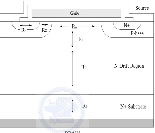
(27) Chapter 3 SiC Power MOSFET. The physics of the operation of power MOSFETs is simpler than that for other power devices because of the absence of minority carrier injection. However, it is necessary to understand the interaction between the cell geometry and the devices characteristics before taking an accurate device design. In the following, the on-state characteristics are first treated followed by analysis of the blocking characteristics.. 3-1 On-resistance The on-resistance is an important device parameter because it determines the maximum current rating. The on-resistance of a power MOSFET is the total resistance between the source and drain terminals in the on-state. The specific on-resistance of silicon carbide power MOSFET’s have been projected to be far superior to their silicon counterparts due to the high breakdown field strength of SiC. The power dissipation in the power MOSFET during current conduction is given by [7]:. 2. where (. PD = I D Ron. (1). PD = JD 2 Ron, sp A. (2). PD ) is the power dissipation per unit area; J D is the on-state current density and A 17.
(28) Ron,sp is the specific on-resistance, defined as the on-resisitance per unit area. These expressions are based upon the assumption that the power MOSFET is operated in its linear region at a relatively small drain bias during current conduction. The maximum power dissipation per unit area is determined by maximum allowable junction temperature and the thermal impedence. The specific on-reisitance of the power MOSFET is determined by the resistance component for the DMOS structure. Fig. 3.1 shows a cross section of a power DMOS MOSFETs structure.. Ron, sp = Rn + + RC + RA + RJ + RD + RS. (3). Where Rn + is the contribution from the N+ source diffusion. RC is the channel resistance, RA is the accumulation layer resistance, RJ is the resistance from the drift region between the p-base region due to JFET pinch-off action, RD is the drift region resistance and RS is the substrate resistance. In a power MOSFET, blocking voltage is supported across the drift layer and thus, drift-region resistance is considered to be minimum possible theoretical limit for the on-resistance of a MOSFET. This assumption is not accurate at lower breakdown voltages where the drift-region resistance RD is compariable to other resistive components and these resistances should also be included in calculating Ron,sp. However, at higher breakdown voltage, RD is significantly higher than other resistances and Ron,sp. could be approximately by. RD. The specific on-resistance of the power MOSFET will then be determined by the drift region alone. Thus:. Ron−sp = Ron−drift. (4). 3-2 The analysis of blocking voltage. 18.
(29) The drift region analysis can be performed to express the relation between the specific on-resistance (Ron) and the blocking voltage capability (VB) of a MOSFET. By approximating the depletion layer in the drift region as an abrupt one-dimension junction, and it is uniform doped ; the doping level NB(cm-3) required to supported a given breakdown voltage VB and depletion width W (cm) at breakdown can be calculated as follows [7]:. NB =. W=. ε ⋅ EB2. (5). 2 ⋅ q ⋅ VB 2VB EB. (6). where VB is the breakdown voltage. The ideal specific on resistance is the resistance per unit area of this layer of material required to support the voltage. Using the above doping and thickness, this given by. 2. Ron ,sp ( ideal ). 4VB W = = q ⋅ N B ⋅ µ ε ⋅ µ ⋅ EB 3. (7). Thus, the ideal specific on-resistance decreases inversely proportional to the mobility and as 3. the cube of the breakdown electric field strength. The denominator ( ε ⋅ µ ⋅ E B ) in Eq. (7) has been referred to as Baliga’s figure of merit (BFOM) for unipolar power devices. In 1983, Baliga drived a figure of merit. BFOM= ε. ⋅ µ ⋅ EB. 3. (8). which defines material parameters to minimize the conduction losses in power MOSFET’s. Here μ is the mobility and EB is the critical electric field of the semiconductor. The BFOM is based upon the assumption that the power losses are solely due to the power dissipation in. 19.
(30) the on-state by current flow through the on-resistance of the power MOSFETs.. 3-3 Material advantages of 4H-SiC for power devices By using the known material properties of semiconductors, it is possible to select those that will exhibit a lower ideal specific on-resistance when compared with silicon by using this expression It has been found that most promising semiconductor are gallium arsenide, whose Baliga’s figure of merit is 12.7 times larger than silicon, and silicon carbide whose Baliga’s figure of merit is 200 times larger than silicon. Although some research has been performed on the fabrication of vertical power MOSFET’s from gallium arsenide, this material has been found to be difficult to work with due to dissociation of the compound during processing. In contrast, silicon carbide offers a such larger improvement in ideal specific on-resistance and is stable even at extremely temperatures.. In the case of Si, the extract dependency of the electron mobility and the breakdown field on the doping concentration is known [23]. 0.91. 5.10 ×10¹⁸ + 92 N B µn = 0.91 3.75 ×10¹⁵ + N B. (9). Based on this known dependence of µ n and EB on the doping concentration for Si power MOSFET’s, a closed form analysis which requires the solution of ionization integral, using an abrupt junction diode, is used for calculating expressions for N B and W for a Si power MOSFET are obtain as [17]. 20.
(31) N B = 2.01× 10¹⁸ VB W = 2.58 × 10 −6 VB. −3 / 4. (10). −7 / 6. Ron− sp = 5.93 × 10 −9 VB. (11) 2.5. (12). the dependency of the breakdown field strength of 4H-SiC and 6H-SiC on N B was determined from the calculated values from [17,9]. The empirical relationship between EB and V B on N B was obtained as. VB. VB. 6 H − SiC. = 6.3 × 10¹⁴ N D. 4 H − SiC. = 7.5 × 10¹⁴ N D. 6 H − SiC. = 1.52 × 10 4 N D. 4 H − SiC. = 1.64 × 10 4 N D. EB. EB. −5 / 7. (13). −5 / 7. (14). 1/ 7. (15). 1/ 7. (16). Table 2.1 provides of N B , W, µ n , and Ron , sp of an ideal DMOS as a function of breakdown voltage for Si and SiC power MOSFET’s. This analysis suggests that 4H-SiC MOSFET would have lower Ron than 6H-SiC. For a given breakdown voltage, Ron for the SiC MOSFET is at least two orders of magnitude smaller than for Si MOSFET, and the ratio of. Ron of the Si MOSFET to that of SiC MOSFET increases with increasing breakdown voltage. Due to the excellent characteristics of SiC, it would be desirable to utilize power MOSFET for high voltage power applications. Unfortunately, the specific on-resistance of the drift region increases very rapidly with increasing breakdown voltage because of the need to reduce its doping concentration and increase its thickness [4]. Thus, in spite of the ability to obtain nearly ideal specific on-resistance with silicon power MOSFET structures, they are not. 21.
(32) satisfactory for applications that require breakdown voltages above 300V due to their high on-state power dissipation. So, many reasons make SiC an attractive candidate for fabricating power devices.. 3-4 Summary The superiority of 4H-SiC illustrated in this chapter is just one of the potential projections in using this wide semiconductor material for high power devices. These advantages in terms of calculated figure of merits provide a motivation for the design and development of power devices on SiC. Despite the unique problems in device fabrication, which many are not yet totally resolved, promising progress in the device development has taken place in the area of power MOSFETs.. 22.
(33) Chapter 4 The electrical performance of SiC MOSFET Silicon-based switching devices have reached the theoretical limitations for high power and for high power and high temperature applications whereas silicon carbide (SiC) has emerged as an alternate material system to overcome the limitations and can be used in extreme environment.. 4-1 Introduction Since SiC is a attractive semiconductor materials for high-power electric devices because they have excellent physical properties such as a wide bandgap, high breakdown voltage, and high saturation electron drift velocity. However, due to higher layer mobility as compared to inversion layer mobility, ACCUFETs emerge as the preferred solution for power MOSFETs on SiC [24]. Channel mobility of power MOSFET’s is one of the most important parameters that determines the on-resistance in the conducting state. More work need to be done to reduce the specific on-resistance and increase the blocking voltage capability in SiC power MOSFEET. The emergence of ACCUFET structures in SiC reveals important advantages in terms of higher channel-carrier mobility [6]. The ACCUFETs structure shows a much promising result in terms of their specific on-resistance compared to the inversion power MOSFET. The main focus in this chapter based on the introduction of design of accumulation-mode power MOSFETs and its optimization using MEDICI two-dimensional device simulator [1].. It should be noted, however, that the contribution and the conclusions in this thesis do 23.
(34) not rely on quantitative results. The methodology used in this paper focuses on the merits of the devices structure itself, independent of the specific parameter values, which are still dominated by different technology imperfections.. 4.2. The trench and planar ACCUFET 4-2-1 The trench ACCUFET Many researchers focus their attention on the SiC MOSFET designed using trench technology, since it offers high channel density and eliminates JFET effect characteristic of DMOS structure. In spite of their advantages, the trench MOSFET have several drawbacks such as high threshold voltage and poor mobility in the channel, which is adversely affects the on-state resistance. Another serve drawback of the trench MOSFET is the gate oxide breakdown, which can occur in off state, under high electric field [8,16].. As it was mentioned earlier, the strongest limitations of SiC trench MOSFET are the dielectric breakdown can occur before semiconductor breakdown. Writing the Gaussian low in the SiC-SiO2 interface. ε SiC ESiC = ε SiO ESiO 2. (1). 2. Considering the ration of dielectric constant of SiC/ SiO2 (9.7/3.9) and ESiC-BR is 3MV/cm ,it is found that the maximum allowable of electric field in the oxide is 7.46x10⁶V/cm. However, due to two-dimensional simulations at the trench corner, the value in the oxide can be higher 24.
(35) than 7x10⁶ V/cm without encountering semiconductor breakdown. Nevertheless, in ordered to have a reliable device, the oxide electric field should be kept under it practical value of 7x10⁶ V/cm.. The simulations of breakdown structure have been shown in the Fig 4.1, drift thickness and concentration are 10μm and 1x1016cm-3 respectively, channel length of 2.0μm, an N+ polysilicon gate electrode over an 100nm thick gate oxide (QF=1x1011 cm-2), an N+ region concentration of 1x1020 cm-3. It has been found that, for a breakdown voltage of 980V, the electric field at the trench corner has the value of 7.8x10⁶ V/cm, consider the theoretical value calculated earlier, it is clear that the device will breakdown because of oxide rupture. To improve this problem, try to wide the trench and round the corner. Because in this way, the curvature of potential lines at the trench corner would be soften [10].. In Table 4.1 the value of electric field as a function of the trench width, for rectangular and rounded corners and a tox of 0.1μm, breakdown voltage of 980V are simulated. As a consequence, by using wide trench in conjunction with rounded trench corners, the electric field in the oxide corner can be kept in the critical value. The influence of gate oxide thickness upon the breakdown voltage has also been investigated. For the rounded trench MOSFETS , breakdown simulation has been carried out, for different oxide thickness and trench width. The simulation results are shown in Table 4.2.. From the results shown in Table 4.2, it can be inferred that there is an inverse proportionality relationship between the oxide thickness and breakdown voltage. Although the simulator does not taken into account the oxide breakdown, we can state that above 7.46x10⁶ V/cm the device breakdown through the avalanche tunneling gate oxide.. 25.
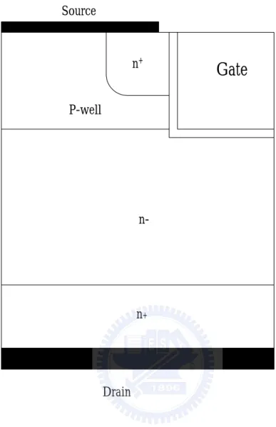
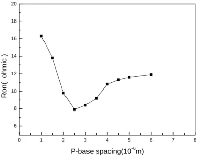
(36) 4-2-2 The planar ACCUFET In silicon, a double-diffused MOSFET (DMOSFET) is the most common structure used for fabricating power MOSFETs [12]. The DIMOS/DMOS structure offers high reliability, ease of integration with ICs and simplicity of fabrication because the gate oxide is shielded from the high electric fields by the adjacent p-type base regions. The cross section of the ACCUFET structure is shown in Fig. 4.2 the n-drift region doping and thickness have been designed to support a high voltage, the entire device is expected to have a high blocking voltage, and since the ACCUFET is a planar device, it does not suffer from any enhanced electric fields, unlike the UMOSFET. In this structure, a thin n-type region is formed below the MOS gate by using a buried p implanted layer. The thickness and doping of this n layer is carefully chosen such that it is completely depleted by the built in potentials of the p /n junction and the MOS gate at zero bias, resulting in a normally-off To obtain reasonable reliability for a device, the electric field in the SiC must be restricted to below 3 MV/cm. The ACCUFET achieves this by suppressing the peak electric field from the surface between SiC and SiO2, to below the p base region [5].. Two different P-base region spacing LP designs were fabricated with different lengths observe the effect of this parameter on the performance of this device. From the simulations, it was found that the electric field near the interface of SiO2 and SiC can be controlled by adjusting When LP was reduced, When LP was reduced, the region above it gets shielded from the high drain voltage thereby reducing the electric field near the oxide. The relationship between P-base spacing (LP) and Ron also be simulated by MEDICI simulator. The dominant sources of on-resistance in an ACCUFET are [14]: the channel resistance of the accumulation layer; the “JFET resistance” between the adjacent P-base regions; and the drift resistance of. 26.
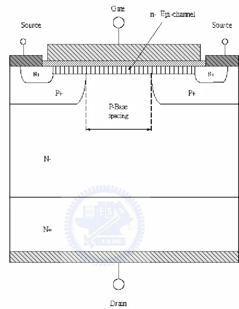
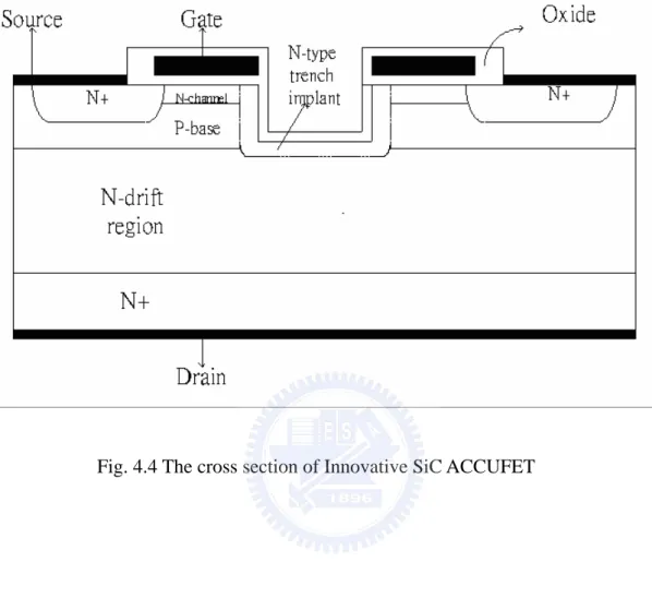
(37) the low doped, voltage-blocking layer. The simulation results of Fig. 4.3 show that a distinct minimum exists for specific on-resistance as is changed from 1 μm to 6 μm. This is because a trade-off exists between the JFET region resistance and the channel resistance. An increase in results in an increase in unit cell pitch, which increases the channel resistance per unit area. On the other hand, as is reduced below 2.5 μm, a dramatic increase in the JFET region resistance occurs because of a reduced current carrying width between adjacent P-base regions [15].. 4-3 The innovative SiC ACCUFET The cross section of the proposed structure is shown in Fig. 4.4 In this structure, a thin N-type region is formed below the MOS gate by using a buried P implanted layer. The thickness and doping of this N-layer is carefully chosen such that it is completely depleted by the built-in potentials of the P+/ N- junction and the MOS gate at zero gate bias, resulting in a normally-off device with the entire drain voltage supported by the P+/N-drift junction. Since this P+/ N- junction can support high voltages. When a positive gate bias is applied, an accumulation channel (of electrons) is created at the interface between SiO2 and SiC. This results in a low resistance path for the electron current flow from the source through the channel, then down to the drain through the drift region to the drain. Assuming that the higher accumulation layer mobility (as compared to the inversion layer mobility) observed in silicon applies to silicon carbide also, a lower on-resistance is expected for the device, which will be referred to as the planar ACCUFET. The main feature of this accumulation type MOSFET is the N-type channel, epitaxially grown on P-base region. Two-dimensional numerical simulations were done using MEDICI with parameters taken from [28] for the ACCUFET structure.. 27.
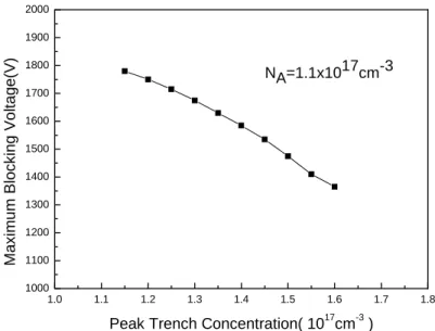
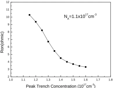
(38) 4-4 Analysis and optimization of device parameters In the following, we will discuss the relationship blocking and driving capability of this structure upon these parameters including, the doping concentration and thickness of P-base layer, and the peak doping concentration of ion-implanted trench region. Two-dimensional numerical simulation structure (including the mesh, the boundaries, and the impurity profiles) for the device was generated in MEDICI. Due to the symmetry of the devices, only half of the device structure was simulated. The structure has a fixed 10μm N-drift region at 1x1017cm-3, an N+ type polysilicon gate electrode with an 100nm thick oxide(QF=1.0x1011cm-2) , a channel length of 2.0μm. The simulation results were used to calculate Baliga’s Figure of Merit (BFOM) as the criterion for structure optimization and comparison.. Peak trench region concentration. We choose the peak concentration of ion-implanted trench region has to be set higher than the P-base concentration (NA). The two P-base concentration 1.1x1017 cm-3, 1.6x1017 cm-3of 2μm thick p-base thick epilayer, were selected. The peak trench concentration of ion-implanted region was varied from 1.15x1017 cm-3 to 1.6x1017 cm-3 for NA = 1.1x1017cm-3, from 1.65x1017cm-3 to 2.1x1017 cm-3 for NA =1.6x1017 cm-3. The simulation results were shown in Fig. 4.5, Fig. 4.6 the maximum blocking voltage was 1780V with NA =1.1x1017 cm-3 with a slightly higher peak trench region concentration of 1.15x1017 cm-3. The maximum operating voltage in this region is determined by the dielectric breakdown before the semiconductor breakdown. When NA =1.6x1017 cm-3, avalanche breakdown occurring in the trench region determines the blocking capability of the device. 28.
(39) From the results, to obtain the maximum operating voltage of the device, also thinking about figure of merit for power devices that is used to optimize the considered parameters. The best trade-off between the breakdown voltage and on-resistance in terms of BFOM is achieved with peak trench region concentration 1.45x1017cm-3for NA =1.1x1017cm-3 . P-base layer thickness. The simulation results of p-base thickness upon blocking voltage, on-resistance are shown in Fig. 4.7.In this simulations, the optimum values of the parameter considered in the previous simulation with peak trench region concentration 1.45x1017cm-3 for NA. =1.1x1017cm-3. As shown in Fig. 4.7, the P-base thickness play an important role on Blocking voltage. The simulation results shows that the p-base epilayer thickness of 2μm is the optimum value in terms of BFOM. Furthermore, we use the same models and parameters in the MEDICI device simulator to obtain and compare the performance characteristics of the structures mention above with innovative ACCUFET. These structures set to have a drift region thickness and concentration 10μm and 1.1x1017 cm-3, respectively, channel length of 2.0μm, an N+-type polysilicon gate electrode over an 100nm thick gate oxide( QF=1.1x1011 cm-2 ) , an N+ region concentration of 1.0x1017cm-3, and a Gaussian doping profile with characteristic width of 0.15μm. The results of simulation are shown as for Table 4.3.The results show clearly that the innovative ACCUFET structure enables a better performance than the trench and planar structure.. 4-5 Summary Power devices made with silicon carbide ( SiC ) are expected show great performance advantages as compared to those made with other semiconductor. Therefore, conventional SiC 29.
(40) MOSFETS suffer high specific on-resistance due to low channel mobility.. The innovative structure of accumulation mode MOSFET for high power applications has been proposed and analyzed in MEDICI. The peak concentration of the ion-implanted trench region strongly influences the breakdown voltage and on-resisitance of the device. To obtain the maximum operating voltage, the peak concentration of the ion-implanted trench region has to be slightly higher than the p-base epilayer. The thickness of p-base epilayer does not play an important role in on-resistance. How ever, it changes the maximum blocking voltage significantly. By using the MEDICI simulator, the best trade off between on-resistance and maximum blocking voltage by setting the thickness of p-base layer precisely. The electrical performances of trench and planar ACCUFET, are mainly limited by the oxide breakdown and p-well spacing.. 30.
(41) Chapter 5. Conclusion. The analysis of 4H-SiC as compared to Si as a semiconductor material for power MOSFET has been shown in favor of 4H-SiC due to its superior material properties. An improvement of two-order magnitude in the specific on resistance of ideal 4H-SiC MOSFET over ideal Si MOSFET is projected. However, a review of the state of the art of SiC power MOSFETs indicates that the performance progress of SiC power devices have been hampered by MOS interface related issues which resulted in high channel resistance and oxide breakdown. Numerical device simulation-based optimization efforts for this novel device have been performed which resulted in optimum device with blocking voltage more than 1.2kV.. Parameter extraction for numerical device simulation of 4H-SiC unipolar devices is the first major topic developed in this thesis. Using 2D numerical device simulation MEDICI , in the models describing electronic devices, the material parameters of Si are replaced by respective parameters of 4H-SiC reported in literature. Using the MEDICI two-dimension simulator, with already existing models to design and optimization of 4H-SiC MOSFETs.. As the main objective of the MOS device research is to bring the channel mobilities in SiC MOS devices as high as the bulk mobilities in SiC and improve reliability of SiO2 layer. The future generation of SiC MOS based devices should the necessary quality dielectric layers and low defect between dielectric and semiconductor interface.. 31.
(42) Reference [1] S. Selberherr, Analysis and Simulation of Semiconductor Devices. New York: Springer-Verlag, 1984. [2] Technology Modeling Associates, inc., TMA MEDICI Two-dimensional Devices Simulation Program ver.2. 3., MEDICI user’s Manial, vol. 1, 1997. [3] B.J. baliga, Modern Power devices, New York: Wiley, 1987. [4] J. wang, and B. W. Williams, “Evaluation of high-voltage 4H-SiC switching devices,” IEEE Trans. Elect. Dev., vol.46,p. 589,1999. [5] P. M. shenoy and B. J. Baliga, “ The planar 6H-SiC ACCUFET: A new high-voltage power MOSFET structure,” IEEE Elect. Dev. Lett ., vol.18, p.589,1997. [6] S.Harada, S. Suzuki, J. Senzaki, R. kosugi, K. Adachi, K. Fukuda, and K. Arau, “High channel mobility in normally-off 4H-SiC buried channel MOSFETs”, IEEE Elect. Dev. Lett., vol. 22, p. 272,2001 [7] B. J. Baliga, “Power semiconductor device figure of merit for high-frquency applications ”, IEEE Elect. Dev. Lett., vol.10,p. 455, 1989. [8] K. G. Pani Dharmawardana and Gehan A. J. Amaratunga, “ Modeling of high current density trench gate MOSFET ”, IEEE Elect. Dev. Lett., vol.47,p. 2420, 2000. [9] R.Raghunathan and b. J. Baliga, “Temperature dependence of hole impact ionization coefficients in 4H and 6H ”, Solid-State Elect., vol. 43, p.199, 1999. [10] K.Shenai, “Optimized trench MOSFET technologies for power devices,” IEEE Trans. Elect. Dev., vol. 39, p. 1435, 1992 [11] C. Lombarbi, S.Mazini, A.Saporito, and M. Vanzi, “ A physical based mobility model for numerical simulation of nonlanar devices” ,IEEE Trans. on Computer-Aided Design, vol. 7, no. 11, p. 1164, 1988. [12] J. N. Shenoy, J. A. Cooper, Jr, and M. R. Melloch, “High-voltage double-implanted power MOSFET’s in 6H-SiC”, IEEE Elect. Dev. Lett ., vol.18, p.93,1997. 32.
(43) [13] M. Ruff, H. Mitlehner, and R. Helbig, “SiC devices: Physics and numerical simulation,” IEEE Trans. Electron Devices, vol. 41, p. 1040, June 1993. [14] R. Singh, D. C. Cpaell, Mirinal K. Das, L. A. lipkin, and John W. Palmour“Development of high-current 4H-SiC ACCUFET ” IEEE Trans. Electron Devices, vol. 50, p. 471, Feb 2003. [15] M. Hasanuzzaman, S. K. Islam, L.M. Tolbert, B.Ozpinect, “Model simulation and verification of a vertical double implanted (DIMOS) transistor in 4H-SiC ”. [16] A. K. Agrarwal, J. B. Casady, L. B. Rowland, W. F. valek, M. H. White, and C. D. Brandt, “1.1kV 4H-SiC power UMOSFET’s”, IEEE Elect. Dev. Lett, vol. 18, p. 586,1997. [17] M.Bhatnagar and B. J. Baliga, “Comparsion of 6H-SiC, 3C-SiC, and Si for power devices”, IEEE Elect. Dev. Lett. , vol.p18, p. 586,1997. [18] R.P.Joshi, “ Monte Carlo caluations of the temperature-and field- dependent electron transport parameters for 4H-SiC ”, J. Appl. Phys., vol.78, p.5518,1995. [19] R. Mickevius, and J. H. Zhao, “ Monte Carlo study of electron transport in SiC ”, Appl. Phys., vol. 83, p. 3161, 1998 [20] W. Fulop, “ Caluation of avalanche breakdown of silicon p-n junctions ”, Solid-State Elect., vol.10, p.39, 1937. [21] C. E. Weitzel, J. W. Plamour, C. H. Carter, K. Moore, K. J. Nordquist, S. Allen, C. Thero, “ silicon carbide High-Power Devices”IEEE Trans. Electron Devices, vol. 43, p. 1732, Oct 1996. [22] E. Arnold and D.Alok, “ Effect of the surface states on electron transport in 4H-SiC inversion layers ”, IEEE Trans. Electron Devices, vol. 48, p. 1870, 2001. [23] C. Jacoboni, C. Canali, G. Ottaviani, and A. A. Quaranta, “A review of some charge transport properties of silicon ”, Solid-State Elect., vol.20, p. 77, 1977. [24] H.Linewih, S.Dimitrijev, C. E. Weitzel, and H. B. Harrison., “ Novel Accumulation-mode power MOSFET ”, IEEE Trans. Electron Devices, vol. 48, p. 1171, 33.
(44) 2001. [25] M. R. Roschke and F. schwierz, “Electron mobility models for 4h, 6H, and 3C SiC ”, IEEE Trans. Electron Devices, vol. 48, p. 1442, 2001. [26] I. A. Khan and j. A. Cooper, J. A. Cooper, Jr., “Measurement of high-field electron transport in silicon carbide”, IEEE Trans. Electron Devices, vol. 47, p. 269, 2000. [27] Handoko Linewih and Sima Dimitrijev., “ Channel-Carrier Mobility Parameters for 4H SiCMOSFETs ” , INTERNATIONAL CONFERENCE ON MICROELECTRONICS , VOL 2,YUGOSLAVIA, 12-15 MAY, 2002 [28] S. Onda,R.Kumar, and K.Hara, “SiC integrated MOSFETs ” Phys. Stat. Sol. Vol.162, p.369,1997.. 34.
(45) Fig.1.1 Applications for power devices in relation to their voltage and current ratings.
(46) Fig.1.2 Lateral n-channel MOSFETs cross section..
(47) Fig. 1.3 The cross section of various power MOSFET structure.
(48) Fig.1.4 The operation of power DMOS.
(49) Fig. 2.1 Low-field electron mobility as a function of doping concentration in 4H-SiC (perpendicular to the c-axis, T = 300 K)..
(50) Fig. 2.2 Drift velocity of electron in 4H-SiC as functions of the applied field..
(51) Fig. 2.3 Mobility between the experimental data and simulation with the parameter values listed in Table 2-2.
(52) Fig. 2.4 Temperature dependence of the coefficients ap and bp for 4H-SiC.
(53) Source. Gate RN+. Rc. N+. RA. P-base RJ. RD. RS. N-Drift Region. N+ Substrate. DRAIN. Fig. 3.1 A cross section of a power DMOS MOSFETs structure.
(54) Source. n+. Gate. P-well. n-. n+. Drain. Fig. 4.1 The cross section of trench MOSFET.
(55) Fig. 4.2 The cross section of accumulation DMOS.
(56) 20. 18. Ron( ohmic ). 16. 14. 12. 10. 8. 6 0. 1. 2. 3. 4. 5. 6. 7. 8. -6. P-base spacing(10 m). Fig. 4.3 The relationship between P-base spacing (LP) and Ron.
(57) Fig. 4.4 The cross section of Innovative SiC ACCUFET.
(58) 2000. Maximum Blocking Voltage(V). 1900. NA=1.1x1017cm-3. 1800 1700 1600 1500 1400 1300 1200 1100 1000 1.0. 1.1. 1.2. 1.3. 1.4. 1.5. 1.6 17. 1.7. 1.8. -3. Peak Trench Concentration( 10 cm ). Fig. 4.5(a) Effect of peak trench-region concentration on maximum operating voltage..
(59) 12 11 17. NA=1.1x10 cm. 10. -3. Ron(ohmic). 9 8 7 6 5 4 3 2 1.0. 1.1. 1.2. 1.3. 1.4. 1.5. 1.6 17. 1.7. 1.8. -3. Peak Trench Concentration (10 cm ). Fig. 4.5(b) Effect of peak trench-region concentration on Ron resistance.
(60) 7.0 6.5. 5.5 17. NA=1.1x10 cm. 5.0. -3. 5. 2. BFOM( 10 V /ohmic). 6.0. 4.5 4.0 3.5 3.0 1.1. 1.2. 1.3. 1.4. 1.5. 1.6 17. 1.7. 1.8. -3. Peak Trench Concentration( 10 cm ). Fig. 4.5(c) Effect of peak trench-region concentration on BFOM.
(61) 1500. Maximun Blocking Voltage (V). 1400. 17 -3 NA=1.6x10 cm. 1300. 1200. 1100. 1000. 900. 800 1.5. 1.6. 1.7. 1.8. 1.9. 2.0. 2.1 17. 2.2. 2.3. -3. Peak trench concentration ( 10 cm ). Fig. 4.6(a) Effect of peak trench-region concentration on maximum operating voltage..
(62) 5.0. 17. 4.5. NA=1.6x10 cm. -3. Ron( ohmic ). 4.0. 3.5. 3.0. 2.5. 2.0 1.6. 1.7. 1.8. 1.9. 2.0. 2.1. 2.2 17. 2.3. 2.4. -3. Peak Trench Concentration( 10 cm ). Fig. 4.6(b) Effect of peak trench-region concentration on Ron resistance..
(63) 6.8. 6.4 -3. 5.6. 5. 2. BFOM( 10 V /ohmic ). 17. NA=1.6x10 cm. 6.0. 5.2. 4.8. 4.4. 4.0 1.6. 1.7. 1.8. 1.9. 2.0 17. 2.1 -3. Peak trench concentration( 10 cm ). Fig. 4.6(c) Effect of peak trench-region concentration on BFOM..
(64) Maximum Blocking Voltage(V). 1800. 1600. 1400. 1200. 1000. 800 1.2. 1.4. 1.6. 1.8. 2.0. 2.2. 2.4. -6. P-base Thickness (10 m). Fig. 4.7(a) Effects of P-base thickness on blocking voltage..
(65) 6.0 5.5 5.0. Ron( ohmic ). 4.5 4.0 3.5 3.0 2.5 2.0 1.5 1.2. 1.4. 1.6. 1.8. 2.0. 2.2. 2.4. -6. P-base Thickness (10 m). Fig. 4.7(b) Effects of P-base thickness on Ron resistance..
(66) 5.5. 5.0. 5. 2. BFOM( 10 V /ohmic ). 6.0. 4.5. 4.0. 3.5. 3.0 1.2. 1.5. 1.8. 2.1. 2.4. -6. P-base Thickness(10 m). Fig. 4.7(c) Effects of P-base thickness on Ron resistance..
(67) Table 1.1 Comparison of Si and SiC material properties.
(68) Table 2.1 Parameter of low field model for 4H-SiC at 300K. Parameter. 4H-SiC. MUN.MIN. 40cm2/Vs. MUN.MAX. 950 cm2/Vs. NRFEN. 2x1017cm-3. ALPHAN. 0.76. Table 2.2 Parameters for 4H-SiC MOSFET mobility models.. parameter Unit μmin cm2/Vs μmax Nref α. 2. cm /Vs cm-3. 4H-SiC 40 950 2x10¹⁷ 0.76. B. 1.0x10⁶. C. 1.74x10⁵. αl. 0.0516. D. V/s. 5.82x10¹⁴.
(69) Table 3.1 Values of doping concentration, electron mobility, drift layer thickness, and specific on-resistance as a function of breakdown voltage for ideal 4H-SiC and Si power MOSFET at room temperature condition.. Breakdown Voltage(V). 200 1000 5000 200 1000 5000 200 1000 5000. Doping Electron Concentration Mobility ( cm −3 ) ( cm 2 / V ⋅ s ) Si 1336 1.72 × 10¹⁵ 14 1356 2.01 × 10 1360 2.35 × 10¹³ 6H-SiC 17 267 1.60 × 10 435 1.81 × 10¹⁶ 15 530 2.04 × 10 4H-SiC 388.95 3.74 ×10¹⁷ 16 745.55 3.93 × 10 905.05 4.13 × 10¹⁵. Width ( µm ) 12.48 81.59 533.44. Specific On-Resistance ( Ω ⋅ cm 2 ) 3.35 ×10 −3 1.88 × 10 −1 1.05 × 101. 1.16 7.69 51.12. 1.69 × 10 −5. 0.75 5.19 35.83. 3.23 × 10 −6. R Si on.sp R SiC on.sp. 200V. 1000V. 5000V. 4H-SiC 6H-SiC. 1037.1 198.2. 1693.1 305.7. 1755.9 355.9. 6.11 × 10 −4. 2.95 × 10 −2. 1.11 × 10 −4 5.98 × 10 −3.
(70) Table 4.1 Oxide electric field in the trench corner as a functions of trench width, for rectangular and round corner.. Trench width(μm). 4. 8. 12. 7.8. 7.1. 6.4. 6.9. 6.3. 5.8. Oxide electric field 6. (10 V/cm) Rectangular corner Oxide electric field 6. (10 V/cm) Rounded corner. Table 4.2 The dependence of the oxide electric field at the trench corner of the oxide.
(71) thickness.. Oxide thickness(μm). 0.1. 0.2. 0.3. 6.3. 5.7. 4.9. 5.8. 5.1. 4.3. Eoxide(106V/cm) Trench width (8μm) Eoxide(106V/cm) Trench width (12μm). Table 4.3 Comparison of ACCUFET structure.
(72) Structure. Trench DIMOS Innovative. MAX.Blocking On-resistance. BFOM. Voltage(V) (Ω). (V2/Ω). 980 1150 1535. 2.48x10⁵ 1.67x10⁵ 5.88x10⁵. 3.87 7.9 4.01.
(73)
數據
+7
相關文件
Teachers may encourage students to approach the poem as an unseen text to practise the steps of analysis and annotation, instead of relying on secondary
How would this task help students see how to adjust their learning practices in order to improve?..
220V 50 Hz single phase A.C., variable stroke control, electrical components and cabling conformed to the latest B.S.S., earthing through 3 core supply cable.. and 2,300 r.p.m.,
In BHJ solar cells using P3HT:PCBM, adjustment of surface energy and work function of ITO may lead to a tuneable morphology for the active layer and hole injection barrier
3: Calculated ratio of dynamic structure factor S(k, ω) to static structure factor S(k) for "-Ge at T = 1250K for several values of k, plotted as a function of ω, calculated
Schematic phase diagram of high-Tc superconductors showing hole doping right side and electron doping left side.. The common Features in
• In 1976 Hawking argued that the formation and evaporation of black holes leads to a fundamental loss of information from the universe, a breakdown of predictability, as
雙極性接面電晶體(bipolar junction transistor, BJT) 場效電晶體(field effect transistor, FET).
