434 IEEE MICROWAVE AND WIRELESS COMPONENTS LETTERS, VOL. 15, NO. 6, JUNE 2005
A Low-Power Low-Phase-Noise LC VCO
With MEMS Cu Inductors
Hsiao-Chin Chen, Chao-Heng Chien, Hung-Wei Chiu, Shey-Shi Lu, Kung-Neng Chang, Kun-Yu Chen, and
Shi-Hao Chen
Abstract—A 2–3 GHz CMOS inductance–capacitance (LC)
voltage-controlled oscillator (VCO) integrated with high-micro-electromechanical systems (MEMS) Cu inductors is reported. While dissipating only 6.3 mW, a phase noise of
121 dBc Hz at 600 kHz offset from 2.78 GHz carrier is
achieved. This MEMS VCO has the largest power-frequency normalized figure-of-merit (12.5 dB) among the Si bipolar and CMOS LC VCOs.
Index Terms—Micro-electromechanical systems (MEMS), voltage-controlled oscillators (VCOs).
I. INTRODUCTION
T
HE integrated inductance–capacitance (LC) voltage-con-trolled oscillators (VCOs) are important building blocks for single-chip communications system. The primary challenge in designing VCOs is minimizing phase noise while maintaining smallest power consumption, which can be achieved by im-proving the poor quality factor ( ) of the on-chip inductors due to silicon substrate losses and series resistance of induc-tors [1]. High ohmic substrates usually provided by bipolar or BiCMOS processes can be adopted to limit the substrate losses [1]. However, for integration of the RF front-end with the dig-ital baseband signal processing, a standard CMOS technology is mandatory [1]. Recently many state-of-the-art integrated LC CMOS VCOs have been implemented in 0.35- m BiCMOS technology [2]–[4]. Even for these fully optimized VCOs, the excellent phase noise performance achieved is still limited by the of the integrated inductors. The other way to break the barrier is to reduce the inductor series resistance, which can be achieved by the use of post-processed Cu inductors, usually fab-ricated by MEMS technology. The attempt [5] in 0.5- m bipolar technology has shown excellent phase noise performance but with a relatively larger power consumption (18 mW) than that ( mW) of CMOS VCOs [2]–[4] implemented in 0.35- m BiCMOS technology. In this work, the performance of an inte-grated LC VCO implemented in standard 0.25- m CMOS with 7- m thick MEMS Cu inductors is reported. It is found that the use of high MEMS Cu inductors improves the performanceManuscript received November 12, 2004; revised December 17, 2004. This work was supported in part by the ROC Ministry of Economic Affairs under Grant 91EC17A05-S10017 and the National Science Council under Grant NSC93-2752-E002-002-PAE and NSC93-2215-E002-028. The review of this letter was arranged by Associate Editor J.-G. Ma.
H.-C. Chen, H.-W. Chiu, and S.-S. Lu are with the Graduate Institute of Elec-tronics Engineering, Department of Electrical Engineering, National Taiwan University, Taipei, Taiwan, R.O.C. (e-mail: sslu@ ntu.edu.tw).
C.-H. Chien, K.-N. Chang, K.-Y. Chen, and S.-H. Chen are with Kuender Incorporation, Taipei, Taiwan, R.O.C.
Digital Object Identifier 10.1109/LMWC.2005.850565
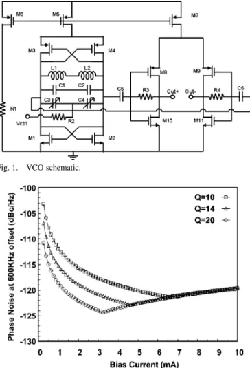
Fig. 1. VCO schematic.
Fig. 2. Phase noise as a function of bias current.
of the integrated LC CMOS VCO substantially in terms of phase noise and power consumption.
II. CIRCUITDESIGN
The schematic of our CMOS VCO is shown in Fig. 1. The double cross-connected nMOS (M1-M2) and pMOS (M3-M4) differential pairs provide the negative resistance. M5 and M7 mirror the pMOS current source (M6) for sourcing the core (M1-M4) and buffer stages (M8-M11). The determination of core bias current ( ) is nontrivial since it depends on the value of the chosen inductor. According to the formula pro-posed in [2], phase noise as a function of with different
values can be plotted as shown in Fig. 2.
Optimal points are different for different values, re-spectively. The minimum phase noise corresponds to the point
CHEN et al.: LOW-POWER LOW-PHASE-NOISE LC VCO 435
Fig. 3. MeasuredQ of the standard and MEMS inductors.
Fig. 4. Perspective view of MEMS VCO.
where the maximum voltage swing is first attained. Further in-crease of results in higher noise with a constant voltage swing and thus phase noise is degraded. In this work, is optimized for the VCO with MEMS Cu inductors.
III. MEMS PROCESSING
VCOs with and without foundry-provided standard alu-minum inductors, which we call STD VCO and MEMS VCO, respectively, were implemented in a standard 0.25- m CMOS process for contrast experiment. The STD VCO and MEMS VCO have the following circuit parameters: transistor size M1-M4: m m, M5: m m, M6: m m, M7: m m, M8-M9:
m m, M10-M11: m m, , and fF. ( ) is 2.5 nH and 1.53 nH for STD VCO and MEMS VCO, respec-tively. The of the foundry provided inductor is at 2.4 GHz while that of the MEMS inductor is as can be seen in Fig. 3, where the measured characteristics of versus frequency are shown. The peak- frequency of the MEMS inductor is 4.8 GHz. To prevent the degradation in tank , the AC coupling capacitance is times smaller than the buffer loading capacitance, which inevitably incurs significant loss in voltage swing. The perspective view of the VCO with the MEMS inductors formed on the die is illustrated in Fig. 4. The 24 m 26 m Metal5 bond pads of the VCOs without
Fig. 5. Die photo of the MEMS VCO.
Fig. 6. VCO tuning range.
foundry-provided inductors are left open for the connection of post-processed MEMS inductors to the underlying core circuitry. The MEMS inductors are fabricated in a commercial MEMS foundry (Kuender Corporation) to achieve the lowest phase noise and power consumption simultaneously. The thick-ness of the electroplated Cu is 7 m. The inductors are spaced from the die by 10- m polyimide. The die photo of the finished MEMS VCO is shown in the Fig. 5. Manufacturing issues, such as electrostatic discharge (ESD), involved with post processing CMOS devices may hinder the use of post-processed MEMS inductors from practical applications and any ESD protection may adversely impact the performance. However, it is found experimentally that the yield of the post-processed VCOs in the 5 mm 5 mm die is 100% even without any ESD protection.
IV. MEASUREDRESULTS ANDDISCUSSION
The core of VCOs draws a current of 2.1 mA from a 3-V supply. The MEMS VCO (STD VCO) operates from 2.78 (2.18) to 3.25 (2.57) GHz, which corresponds to a center frequency of 3.02 (2.38) GHz and a tuning range of 15.6% (16.4%), as shown in Fig. 6. The higher oscillation frequency of MEMS VCO is due to the smaller inductance used. The substrate capacitance of
436 IEEE MICROWAVE AND WIRELESS COMPONENTS LETTERS, VOL. 15, NO. 6, JUNE 2005
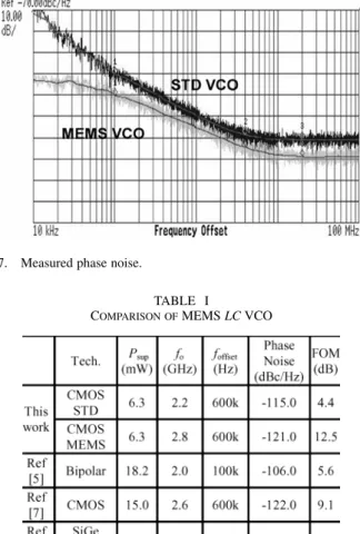
Fig. 7. Measured phase noise.
TABLE I
COMPARISON OFMEMS LC VCO
the MEMS inductor with 10- m thick polyimide is reduced and hence can also contribute to the increase of the center frequency. The carrier power of MEMS VCO and STD VCO are 14.42 and dBm, respectively, evidencing a higher is deed achieved in MEMS VCO due to the use of thick Cu in-ductor. The oscillator phase noise is measured by using Agi-lent E4440A spectrum analyzer with phase-noise measurement utility in a shielding room. The plots of the phase noise versus the offset frequency from 2.78-GHz carrier (MEMS VCO) and the 2.18-GHz carrier (STD VCO) are shown in Fig. 7. The flat-tening off of the straight curves for larger offset frequencies ( MHz) is due to the limited dynamic range of the system [1].
The MEMS VCO shows a phase noise of dBc Hz at 600 kHz offset while dissipating only 6.3 mW. The achieved phase noise performance is benchmarked to the STD VCO that realizes a phase noise of dBc Hz at 600 kHz offset. For fair comparison of VCOs with different oscillation
fre-quencies and power consumptions ( ), the widely-accepted power-frequency-normalized figure-of-merit (FOM) [2], [6] given below is calculated and summarized in Table I for the recently reported 2–3 GHz band MEMS LC-VCOs [5], [7], [8] along with the VCOs of this work.
(1) where represents the phase noise at an offset frequency from the carrier frequency . When compared to the STD VCO, our MEMS VCO has an 8.1 dB improvement in FOM at 600-kHz offset due to the use of high MEMS Cu inductors. The current consumption (2.1 mA) of our MEMS VCO core seems to be on the high-side compared to that (125 A) of [8]. Nevertheless, the achieved FOM of this work is quite compa-rable to that of [8]. The MEMS VCO has the largest FOM of 12.5 dB among the GHz-band Si bipolar and CMOS in-tegrated LC VCOs.
V. CONCLUSION
VCOs with post processed MEMS inductors and foundry-provided aluminum inductors were implemented in a 0.25- m CMOS process for comparison. It is found that the MEMS VCO shows an 8.1 dB improvement of power-frequency-normalized figure-of-merit than the standard VCO.
REFERENCES
[1] J. Craninckx and M. Steyaert, Wireless CMOS Frequency Synthesizer
Design. Norwell, MA: Kluwer, 1998.
[2] D. Ham and A. Hajimiri, “Concepts and methods in optimization of integrated LC VCOs,” IEEE J. Solid-State Circuits, vol. 36, no. 6, pp. 896–909, Jun. 2001.
[3] R. Aparicio and A. Hajimiri, “A noise-shifting differential colpitts VCO,” IEEE J. Solid-State Circuits, vol. 35, no. 12, pp. 1728–1736, Dec. 2002.
[4] A. Ismail and A. A. Abidi, “CMOS differential LC oscillator with sup-pressed up-converted flicker noise,” in ISSCC Dig. Tech. Papers, Feb. 2003, pp. 98–99.
[5] J. W. M. Rogers, V. Levenets, C. A. Pawlowicz, N. G. Tarr, T. J. Smy, and C. Plett, “Post-processed Cu inductors with application to a completely integrated 2-GHz VCO,” IEEE Trans. Electron Devices, vol. 48, no. 6, pp. 1284–1287, Jun. 2001.
[6] J. Rael and A. A. Abidi, “How to design an LC oscillator first time right,” in Proc. ISSCC RF CMOS Short Course, Feb. 2001.
[7] E.-C. Park, J.-B. Yoon, S. Hong, and E. Yoon, “A 2.6 GHz low phase-noise VCO monolithically integrated with highQ MEMS inductors,” in
Proc. ESSCIRC’02 Conf., 2002, pp. 143–146.
[8] V. K. Saraf, D. Ramachandran, A. Oz, G. K. Feder, and T. Mukherjee, “Low-power LC-VCO using integrated MEMS passives,” in Proc. IEEE
Radio Frequency Integrated Circuits (RFIC’04) Symp., Jun. 2004, pp.