Self-Matched ESD Cell in CMOS Technology for
60-GHz Broadband RF Applications
Chun-Yu Lin
1, Li-Wei Chu
1, Ming-Dou Ker
1,2, Tse-Hua Lu
3, Ping-Fang Hung
3, and Hsiao-Chun Li
3 1National Chiao-Tung University, Hsinchu, Taiwan
2
I-Shou University, Kaohsiung, Taiwan
3Taiwan Semiconductor Manufacturing Company
Abstract — A self-matched ESD cell library has beenimplemented in a commercial sub-100nm CMOS process for 60-GHz broadband RF applications. This ESD cell library has reached the 50-Ω input/output matching to reduce the design complexity for RF circuit designer and to provide suitable electrostatic discharge (ESD) protection. Experimental results of this ESD cell library have successfully verified the ESD robustness and the RF characteristics in the 60-GHz frequency band. This self-matched ESD cell library is easily to be used for ESD protection design in the 60-GHz broadband RF applications.
Index Terms — Broadband, electrostatic discharge (ESD), ESD cell, V-band, 60 GHz.
I. INTRODUCTION
With the scaling-down feature size, improving high-frequency characteristics, low power consumption, high integration capability, and low cost for mass production, the nanoscale CMOS technology has been used to implement RF circuits. However, the thinner gate oxide in nanoscale CMOS technology seriously degrades the electrostatic discharge (ESD) robustness of IC products. Therefore, on-chip ESD protection circuits must be added at all input/output ports in RF IC against ESD damages [1]. To minimize the impacts from ESD protection circuit on RF performances, the ESD protection circuit at input/output ports must be carefully designed. Several ESD protection designs have been reported for RF circuits [2], [3]. As the operating frequencies of RF circuits are increasing, on-chip ESD protection designs for RF applications are more challenging.
The frequency band of 57~64 GHz has been allocated for unlicensed usage in the next-generation wireless communications. RF circuits operating at this 60-GHz band have the benefits of excellent interference immunity, high security, multi-gigabit speed, and frequency re-usable. Recently, several CMOS transceivers operating at this frequency band have been reported. Some ESD protection designs for the circuits operating at this frequency band were also presented [4], [5]. In the ESD protection design in [4], the on-chip inductor is used to
resonate with the capacitive ESD diode to form a series LC resonator. At frequencies above the resonant frequency of the series LC resonator, the impedance becomes large, which means the signal loss from the ESD protection circuit is reduced. Hence, the series LC resonator can be used to protect the 60-GHz circuits. However, the transient voltage across the RF circuits under ESD stress is the total voltage drop across the inductor and the diode. To improve ESD robustness of the RF circuits, the transient voltage across the RF circuits under ESD stress must be reduced, especially for the circuits realized in nanoscale CMOS technology. In another ESD protection design in [5], ESD inductor is co-designed with the 60-GHz power amplifier. The ESD inductor acts part of the RF matching network. Of course, the ESD inductor has been carefully designed to provide ESD current path.
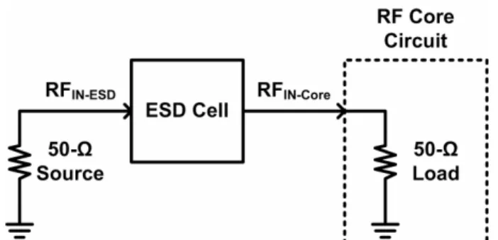
To reduce the design complexity for RF circuit designer, a self-matched ESD-protection cell library in CMOS technology for 60-GHz broadband RF applications is implemented in this work. As shown in Fig. 1, this ESD cell library has reached the 50-Ω input/output matching. Such ESD cell library has been verified in a commercial sub-100nm CMOS process to verify its ESD robustness and broadband RF performances.
Fig. 1. Self-matched ESD cell for 60-GHz broadband RF applications.
978-1-4244-6241-4/978-1-4244-6242-1/
978-1-4244-6243-8/10/$26.00 © 2010 IEEE 2010 IEEE Radio Frequency Integrated Circuits Symposium
RTUIF-20
II. ESDCELL DESIGN
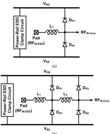
The distributed ESD protection scheme is used to implement the ESD cells in this work to provide broadband impedance matching around 60 GHz [6], [7]. This ESD cell library provides four ESD cells with
different
ESD robustness, as listed in Table I. These four ESD cells are designed to sustain 0.5-, 1-, 1.5-, and 2-kV human-body-model (HBM) ESD tests, respectively. Fig. 2(a) shows the circuit diagrams of the 0.5- and 1-kV cells with 1-stage ESD protection. The 1-stage ESD protection is designed with a low-C pad, an on-chip spiral inductor, and a pair of ESD diodes. Similarly, the circuit diagrams of the 1.5- and 2-kV cells with 2-stage ESD protection are shown in Fig. 2(b). The 2-stage ESD protection is designed with a low-C pad, two on-chip spiral inductors, and two pairs of ESD diodes. Besides, the power-rail ESD clamp circuit is added in each ESD cells to provide ESD current paths between VDD and VSS. AnRC-inverter-triggered NMOS with ~2000-μm width is used as the power-rail ESD clamp circuit in this work. Since the power-rail ESD clamp circuit is placed between VDD and
VSS, it does not contribute any parasitic effects to
input/output ports. When the positive-to-VDD
(negative-to-VSS) ESD stress occurs at the pad, the ESD current can be
discharged through the diodes DP (DN) from the pad to
VDD (VSS). Under positive-to-VSS (negative-to-VDD) ESD
stress, the ESD current path consists of the diodes DP (DN)
and the power-rail ESD clamp circuit. The ESD cells can provide the corresponding current discharging paths under all ESD stress modes.
The design parameters of the ESD cells are listed in Table I. The RF characteristics of the ESD cells are simulated by using the microwave circuit simulator ADS with layout parameters. A signal source with 50-Ω impedance drives the RFIN-ESD of the cell, and a 50-Ω load
is connected to RFIN-Core to simulate the RF circuit. The
reflection (S11) parameters are shown in Fig. 3(a). These
ESD cells exhibit good input matching (S11 < -12 dB)
among 57~64 GHz. The transmission (S21) parameters are
compared in Fig. 3(b). At 60-GHz frequency, the 0.5-, 1-, 1.5-, and 2-kV cells have about 0.8-, 1.3-, 1.6-, and 2.2-dB power loss, respectively.
(a)
(b)
Fig. 3. Simulation results of ESD cells on (a) S11, and (b) S21,
parameters. (a)
(b)
Fig. 2. Circuit diagrams of ESD cells with (a) 1-stage ESD protection and (b) 2-stage ESD protection.
One set of these test circuits are arranged with G-S-G style in layout to facilitate the on-wafer RF measurement. Besides, another set of the test circuits are implemented with the RF-NMOS emulator, as shown in Fig. 4. The ESD robustness of the ESD-protected RF circuits can be estimated by the ESD cell with the RF-NMOS emulator. All test circuits have been fabricated in a commercial sub-100nm CMOS process for RF and ESD verifications. Fig. 5 shows the die photos of the 1- and 2-kV cells.
III.EXPERIMENTAL RESULTS
A. RF Performances
The S-parameters of these four ESD cells have been measured around 60 GHz. The voltage supply of VDD (VSS)
is 1.2 V (0 V), and the input dc bias is 0.6 V. The source and load resistances to the test circuits are kept at 50 Ω.
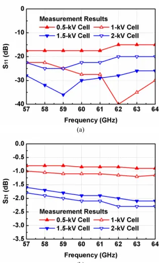
The measured S11 and S21 parameters versus frequency are
shown in Figs. 6(a) and 6(b), respectively. As shown in Fig. 6(a), these ESD cells exhibit good input matching (S11 < -20 dB) among 57~64 GHz. At 60-GHz frequency,
the 0.5-, 1-, 1.5-, and 2-kV cells have about 0.9-, 1.1-, 1.9-, and 2.1-dB power loss, respectively. The measurement results of the ESD cells are well matching to the simulation results. Hence, applying these ESD cells to RF circuits, the performances can be exactly simulated during the design phase of the RF circuits.
B. ESD Robustness
The HBM ESD robustness of the fabricated ESD cells with the RF-NMOS emulators are evaluated by the ESD tester in human body model (HBM). The positive-to-VDD
(PD-mode), positive-to-VSS (PS-mode), negative-to-VDD
(ND-mode), and negative-to-VSS (NS-mode) ESD
robustness of each ESD cells are listed in Table I. The 0.5-, 1-, 1.5-, and 2-kV cells can sustain 0.75-, 1.5-, 2.25-,
(a)
(b)
Fig. 6. Measurement results of the fabricated ESD cells on (a) S11, and (b) S21, parameters.
Fig. 4. RF-NMOS emulator to verify ESD protection effectiveness of the proposed ESD cell.
(a)
(b)
Fig. 5. Die photos of (a) 1-kV cell and (b) 2-kV cell.
and 2.5-kV HBM ESD tests, respectively. These ESD test results are even better than the original specification of these ESD cells. Besides, the power-rail ESD clamp circuit can sustain over 8-kV HBM ESD tests.
IV.CONCLUSION
The ESD cells for 60-GHz broadband RF applications are presented in this work. These ESD cells have reached the 50-Ω input/output matching. This ESD cell library reduces the design complexity for RF circuit designer and provides suitable ESD protection. Verified in a commercial sub-100nm CMOS process, the 0.5-, 1-, 1.5-, and 2-kV cells have about 0.9-, 1.1-, 1.9-, and 2.1-dB power loss, respectively. Besides, they can sustain 0.75-, 1.5-, 2.25-, and 2.5-kV HBM ESD tests, respectively. This ESD cell library is developed to support foundry’s customers for them to easily apply ESD protection in the 60-GHz broadband RF circuits.
ACKNOWLEDGEMENT
This work was supported by Taiwan Semiconductor Manufacturing Company (TSMC). The authors would like to thank Mr. C.-P. Jou, Mr. H.-H. Chen, Mr. M.-H. Tsai, Mr. T.-L. Hsu, Mr. M.-H. Song, Mr. J.-C. Tseng, and Mr. T.-H. Chang, of TSMC for their technical discussion to this study. The authors would also like to thank the support from “Aim for the Top University Plan” of the
National Chiao-Tung University and Ministry of Education, Taiwan.
REFERENCES
[1] S. Voldman, ESD: RF Technology and Circuits. John Wiley & Sons, 2006.
[2] C.-Y. Lin and M.-D. Ker, “Low-capacitance SCR with waffle layout structure for on-chip ESD protection in RF ICs,” in Proc. IEEE Radio Frequency Integrated Circuit
Symp., 2007, pp. 749-752.
[3] M.-D. Ker and Y.-W. Hsiao, “On-chip ESD protection strategies for RF circuits in CMOS technology,” in Proc.
Int. Conf. Solid-State and Integrated Circuit Technology,
2006, pp. 1680-1683.
[4] B. Huang, C. Wang, C. Chen, M. Lei, P. Huang, K. Lin, and H. Wang, “Design and analysis for a 60-GHz low-noise amplifier with RF ESD protection,” IEEE Trans.
Microwave Theory and Techniques, vol. 57, no. 2, pp.
298-305, Feb. 2009.
[5] S. Thijs, K. Raczkowski, D. Linten, M. Scholz, A. Griffoni, and G. Groeseneken, “CDM and HBM analysis of ESD protected 60 GHz power amplifier in 45 nm low-power digital CMOS,” in Proc. EOS/ESD Symp., 2009, pp. 329-333.
[6] M.-D. Ker and B.-J. Kuo, “Decreasing-size distributed ESD protection scheme for broadband RF circuits,” IEEE
Trans. Microwave Theory and Techniques, vol. 53, no. 2,
pp. 582-589, Feb. 2005.
[7] M.-D. Ker and C.-M. Lee, “ESD protection circuits with impedance matching for radio-frequency applications,” US Patent 2006/0256489 A1, Nov. 16, 2006.
TABLE I
DESIGN PARAMETERS AND MEASUREMENT RESULTS OF ESDCELLS
0.5-kV Cell 1-kV Cell 1.5-kV Cell 2-kV Cell
L1 0.13 nH 0.13 nH 0.1 nH 0.1 nH DP1 8 μm / 0.6 μm 15 μm / 0.6 μm 13 μm / 0.6 μm 17 μm / 0.6 μm DN1 8 μm / 0.6 μm 15 μm / 0.6 μm 13 μm / 0.6 μm 17 μm / 0.6 μm L2 N/A N/A 0.06 nH 0.06 nH DP2 N/A N/A 10 μm / 0.6 μm 13 μm / 0.6 μm DN2 N/A N/A 10 μm / 0.6 μm 13 μm / 0.6 μm Design Parameters Cell Area 130 μm x 210 μm 130 μm x 210 μm 110 μm x 280 μm 110 μm x 280 μm S11 at 60 GHz < -15 dB < -25 dB < -25dB < -20 dB S22 at 60 GHz ~ 0.9 dB ~ 1.1 dB ~ 1.9 dB ~ 2.1 dB PD-Mode HBM 1 kV 2 kV 2.75 kV 3.5 kV PS-Mode HBM 1 kV 1.75 kV 2.25 kV 2.5 kV ND-Mode HBM 0.75 kV 1.5 kV 2.25 kV 2.75 kV Measu remen t Resu lts NS-Mode HBM 0.75 kV 1.5 kV 2.25 kV 2.75 kV 576