國
立
交
通
大
學
機械工程學系研究所
博 士 論 文
電漿處理對奈米碳管合成及奈米碳管表面特性
之影響
The Effect of Plasma Treatment on the Synthesis
and Surface Characteristics of Carbon Nanotubes
研 究 生:溫華強
指導教授:周長彬 教授
吳文發 博士
電漿處理對奈米碳管合成及奈米碳管表面特性之影響
The Effect of Plasma Treatment on the Synthesis and Surface
Characteristics of Carbon Nanotubes
研 究 生:溫華強 Student:Hua-Chiang Wen
指導教授:周長彬 Advisor:Prof. Chang-Pin Chou
吳文發 Advisor:Dr. Wen-Fa Wu
國 立 交 通 大 學
機械工程學系
博 士 論 文
A Thesis
Submitted to Institute and Department of Mechanical Engineering National Chiao Tung University
in partial Fulfillment of the Requirements for the Degree of
Ph.D in
2007
Hsinchu, Taiwan, Republic of China
電漿處理對奈米碳管合成及奈米碳管表面特性之影響
學生:溫華強 指導教授:周長彬 教授
吳文發 博士
國立交通大學工學院 機械工程系﹙研究所﹚博士班
摘要
近年來,在矽元件尺寸微小化的趨勢下,奈米碳管特別被期待應用在奈米電 子元件上,此乃因奈米碳管具有極佳的特性。本論文試圖提出電漿處理運用於奈 米碳管的研究,將實驗結果中包括前處理與成長特性、表面特性、電子傳輸能力、 與機械特性作連貫性的探討。 在前處理與成長特性部分,氫電漿前處理,可促使微小顆粒產生聚集,依據 對鎳層觸媒前處理產生之效應,證明週期時間、氫氣流量對於顆粒化有其對應的 趨勢。經由拉曼光譜儀的量測,合成後的奈米碳管在適當條件下的氫電漿前處理 可使非晶質碳與非序結構降低,進而提升奈米碳管之品質。此外,藉由奈米壓痕 壓縮測試,從壓力控制模式,可發現到奈米顆粒之楊氏模數與硬度值皆比鎳層為 低,因而證實前處理奈米顆粒的特性。 在表面特性上,經由四氟化碳與氧氣電漿後處理,奈米碳管表面非晶質碳明 顯降低。由拉曼光譜儀顯示,短時間之後處理可提升品質比值,而長時間卻降低 品質比值。此外,傅立葉光譜儀可證實表面存在碳氧與碳氟的鍵結。由熱脫附量 測顯示出,奈米碳管表面氟氧鍵確實有脫附的現象。X 光電子能譜亦印證出表面 確實具有氟化之增益。 在電子傳輸研究中,以曝光顯影製作橫向之結構,讓奈米碳管連接於兩邊之 電極。藉由四氟化碳與氧氣電漿後處理,證實電漿後處理確實具有修飾奈米碳管 與增進電子傳輸之效益,而使得元件在室溫下可表現出蕭特基(Schottky)接觸特性。 至於機械特性部分,本論文選用奈米壓痕針頭對頂部奈米碳管薄膜作測試, 可得到相對的韌性並展現出奈米碳管薄膜的特點。此外,利用拉曼光譜儀量,印證當增加施力所產生的裂痕越大,量測品質變化量(ID/IG)上升,由此可印證奈米碳
管之非序結構確實提升。
整體實驗中,無論是觸媒的形成,奈米碳管的吸附能力,電性、機械方面的 測試上,均可藉由實驗證實其特性。
The Effect of Plasma Treatment on the Synthesis and Surface Characteristics of Carbon Nanotubes
Student:Hua-Chiang Wen Advisors:Prof. Chang-Pin Chou
Dr. Wen-Fa Wu
Institute and Department of Mechanical Engineering, National Chiao Tung University
ABSTRACT
In the semiconductor industry, silicon devices are being scaled down to smaller dimensions. Carbon nanotubes (CNT) are of particular interest for future nanoelectronic applications, because of their high aspect ratio, small radius of curvature, high chemical stability, and large mechanical strength. Plasma surface treatments are promising techniques in the design and development of new materials because surfaces can be modified without altering the bulk properties of the material. Accordingly, more sensitive surface analysis approaches are being used to obtain more precise information regarding the plasma-treated surface chemistry. An experiment was conducted to elucidated pretreatment, the adsorption (desorption) in plasma surface treatment, the electronic conduction property associated with surface treatments, and the mechanical characteristics of CNTs.
In the pretreatment, CNTs were synthesized by microwave plasma chemical vapor deposition (MPCVD) on Ni/TiN/Si and Ni/TaN/Si systems. The effect of the pretreatment period and flow rate on the growing characteristics of the Ni catalyst layer and the properties of the CNTs was examined. The mechanical response of particle aggregates to the compression of substrates is emphasized. The improvement of the surface performance of the catalyst is using H2 plasma is suggested. Therefore, small
agglomerates of catalyst nanoparticles formed on TiN buffer substrates, helping to elucidate the mechanical properties of relatively large pretreated nanoparticles. The deformation behavior of the agglomerates under loaded control-mode nanoindentation was investigated. Nanoparticle testing demonstrated a lower modulus (from 238.9±8.4
to 176.2±6.1 GPa) and hardness (from 17.2±1.6 to 11±0.8 GPa) than those of the Ni film. The effects of the H2 plasma flow rate during pretreatment on the synthesis of
CNTs using an MPCVD system are also studied. Raman spectroscopy was employed with a change-coupled detector is used to elucidate the effect of the flow rate on the intensity ratio of G and D bands (ID/IG), which in turn yields the amounts of amorphous
carbon and carbonaceous particles in the CNTs.
The effect of CF4/O2 plasma on the surface performance of CNTs in the
post-treatment is elucidated. SEM and TEM studies reveal changes in the surface morphologies of CNTs that were exposed to the CF4/O2 plasma. Additionally, the ID/IG
ratios reveal that chemical treatment with CF4/O2 plasma for 2 min reduces the degree
of disorder. After 10 min, however, the degree of disorder in CNTs is increased. FTIR absorption spectra include peaks that correspond to C-O and C-F stretching vibrations. The TDS results yield adsorption information. XPS datum reveals fluorination in CF4/O2 plasma-treated CNTs and the absence of a significant of physisorbtion on CNTs.
This result shows that adding oxygen to the plasma increases the decomposition efficiency.
A CNT bridge on SiO2 that is patterned photolithographically in an electronic
device is described. The CNTs grow laterally to the substrate over a Ta vertical growth barrier and connect to the side of the electrode pad. The CF4/O2 post-treated has a
higher current-voltage curve than the surface-modified. The typical Schottky contact characteristics at room temperature are discussed. The surface of the CNT interacts with the surrounding plasma, breaking C-C bonds and creating active sites to bond the functional groups (fluorination). C-F binding in the amorphous carbon can be reduced by modifying the CNTs.
A CNT film was studied using nanoindentation equipment (Berkovitch indenter) by varying the loading force. CNT films exhibit features that are associated with toughening against cracks caused by indentation. The quantitative indentation force is utilized to determine the CNTs axial modulus, depending on the Raman shift. The ID/IG
ratios of the CNTs films are associated with an increase in the force. Such features follow in part from the fact that CNTs films generally contain some disordered regions.
The experiment on plasma treatments yields information on the formation of the catalyst, the adsorption (desorption) capacity, the electronic conduction and the
Contents
Abstract (in Chinese) ··· i
Abstract (in English) ··· iii
Contents··· vi
Table Lists··· viii
Figure Captions ··· ix
Chapter 1 Introduction··· 1
1-1 A brief History of nanomaterials ··· 1
1-1-1 Buckminsterfullerene··· 1
1-1-2 The origin of carbon nanotubes ··· 1
1-1-3 Single-walled nanotubes··· 2
1-1-4 The graphite structure of carbon nanotubes··· 3
1-1-5 The potential of carbon nanotubes··· 4
1-2 Motivation ··· 5
1-2-1 The role of carbon nanotubes··· 5
1-2-2 Objective··· 6
Chapter 2 Literature review··· 8
2-1 Introduction··· 8
2-2 Structures of carbon nanotube··· 8
2-3 Characteristics of carbon nanotube··· 13
2-3-1 Mechanical properties ··· 13
2-3-2 Electronic properties ··· 16
2-3-3 Quantized conductance ··· 19
2-3-4 Thermal properties··· 21
2-3-5 Magnetic fields properties··· 23
2-3-6 Field emission··· 24
2-3-7 Biology and nanotube··· 25
2-4 The method of carbon nanotubes synthesis ··· 26
2-4-1 Arc-discharge methods··· 26
2-4-2 Laser vaporization ··· 26
2-4-3 Chemical vapor deposition··· 27
2-5 The mechanism of carbon nanotubes growth··· 28
2-5-1 The diffusion path of carbons atom··· 28
2-5-2 Tip growth mode and base growth (root growth) mode··· 28
Chapter 3 Experimental apparatus and procedures··· 59
3-1 Experimental procedures··· 59
3-2 Deposition system··· 64
3-3 Measurement system··· 64
Chapter 4 Primary result··· 72
4-1 Characterization of carbon nanotubes density through Ni nanoparticle formation using hydrogen plasma treatment on the TiN buffer layer and nanoindentation··· 72
4-1-1 Introduction··· 72
4-1-2 Results and discussion··· 74
4-1-2-2 Indentation of catalyst from pretreatment··· 75
4-1-3 Conclusion··· 78
4-2 Effects of hydrogen plasma pretreatment on the TaN buffer layer for growth of carbon nanotubes···80
4-2-1 Introduction··· 80
4-2-2 Results and discussion··· 82
4-2-3 Conclusions··· 85
4-3 Effects of fluorocarbon/oxygen plasma post-treatment on the surface performance of multiwalled carbon nanotubes···87
4-3-1 Introduction··· 87
4-3-2 Results and discussion··· 88
4-3-3 Conclusion··· 93
4-4 Effect of fluorocarbon/oxygen plasma post-treatment on the ··· 94
lateral carbon nanotubes··· 4-4-1 Introduction··· 94
4-4-2 Results and discussion··· 95 4-4-2-1 SEM and AFM ··· 95
4-4-2-2 XPS spectra··· 96
4-4-2-3 I-V analysis··· 97
4-4-3 Conclusion··· 98
4-5 Characteristics of indentation on carbon nanotubes films··· 99
4-5-1 Introduction··· 99
4-5-2 Results and discussion··· 100
4-5-3 Conclusion··· 101
Chapter 5 Conclusions and future work··· 140
5-1 Conclusions··· 140
5-2 Future work··· 141
LIST OF TABLES
Table 4-1 The summarized that the RMS surface roughness of the catalytic-layer changed from 6.1 to 11.9 nm, as the pretreatment time increased from 3 to 15 minutes.··· 103 Table 4-2 (a) Ni/TiN/Si thin film and (b) Ni particles/TiN/Si indented with low
force. The particles were observed only inside the indented parts, thus lead the decreased in modulus and hardness. ···103
LIST OF FIGURES
Figure 2-1 Perspective view of a rope of (10,10) carbon nanotubes. ··· 29 Figure 2-2 Atomic structure and spectroscopy of metallic SWNTs STM
images. ··· 29 Figure 2-3 HRTEM image of two nanotubes with outer diameters of 6 nm and 16
nm. ··· 30 Figure 2-4 (a) armchair, zigzag, and chiral SWNTs. (b) Tunneling electron
microscope image of a 1.3-nm-diameter chiral SWNT. (c) Transmission electron microscope (TEM) image of a MWNT. ··· ···· 31 Figure 2-5 Nanotube coordinates. ··· ··· 31 Figure 2-6 Calculated one-dimensional electronic density of states on single-wall
nanotubes. ··· ··· 32 Figure 2-7 Relation between the hexagonal carbon lattice and the chirality of
carbon nanotubes. ··· ··· 33 Figure 2-8 (a) Characterization of CVD nanotube tips. (b) Transmission electron
microscope (TEM) image of a CVD nanotube tip. (c) Tip oscillation amplitude (d) Imaging IgM macromolecules with a CVD nanotube tip at high resolution. ···34 Figure 2-9 High-resolution electron microscope image of a 4 Å tubule (side walls
are marked by lines) confined inside an 18-shell carbon nanotube.··· 35 Figure 2-10 Diamond and Graphite structures. ··· ··· 36 Figure 2-11 (a) A conducting AFM tip is used to measure the resistance of the
NT-HOPG interface. (b) The NT is in registry. (c) The NT Fermi-level states (dotted arrow). ··· ···36 Figure 2-12 (a) A tube that has been rotated through 180¡. (b) More dense data
over one period on a different tube gives us a better indication of the shape of the curve. ··· 37 Figure 2-13 In a metallic carbon nanotube, left-moving electrons (red) and
right-moving electrons (blue) belong to two different bands with distinct microscopic structures. ··· ··· 38 Figure 2-14 (a) Typical atomically resolved STM image of a (15,0) SWNT. Scale
bar, 1 nm. (b) Tunneling conductance data (c) Typical high-resolution normalized conductance (dI/dV )/(I/V) curves and measured I-V curves.··· ··· 39 Figure 2-15 (a) A dry ribbon deposited on a glass substrate. (b) A nanotube fiber
(scale bar 5 25 mm). (c) Cross section of a nanotube fiber. (scale bar 5 16.7 mm). (d) Magnification of the bright region in (c) (scale bar 5 1 mm). ··· 40 Figure 2-16 Mechanical measurements under tensile loading performed at a strain
rate of 1% per minute. ··· 40 Figure 2-17 (a) An SEM image of two AFM tips holding a MWCNT.(b)
High-magnification SEM image of the indicated region in (a), showing the MWCNT between the AFM tips. (c) Higher magnification SEM image.···41 Figure 2-18 (a) Schematic showing the principle of the tensile-loading experiment.
(b) Plot of stress versus strain curves for individual MWCNTs. ···41 Figure 2-19 (a) SiC NRs or carbon nanotubes (b) Optical micrograph of a sample
bending with an AFM tip. The tip (blue triangle).··· 42
Figure 2-20 (a)Surface plot showing the F-d responseof a 23.0-nm-diameter SiC NR (b) Dependence of the force constant k(x) on position x along the axis of the same NR.··· 43
Figure 2-21 (a) Device viewed from above. Preparation of samples involves chemical vapour deposition of SWNTs (b), AFM image of an SWNT (c). Side-view of the AFM pushing experiment.··· 44
Figure 2-22 (a) Experimental result of conductance. (b) Conductance versus band energy calculated for an ideally contacted (5,5) SWNT. (c),(d). Simulated atomic configurations of the nanotube pushed to 78 and 158 respectively. ··· 45
Figure 2-23 CESR (conduction electron spin resonance) of SWNT bucky paper films electrochemically doped by K for K C various x compositions.··· 46
Figure 2-24 Schematic of three types of MWNT (a) intershell intercalation; (b) no reaction; (c) intercalation-assisted break-up. ··· 47
Figure 2-25 (a) Schematic illustration of the generation of a nanotube (b) Top: Band-structure of the 2D graphene sheet (in gray). ··· 48
Figure 2-26 Time-dependence of the current flowing through a multi-walled nanotube during current-induced breakdown. ··· 48
Figure 2-27 A wave hitting two partially reflective barriers. ··· 49
Figure 2-28 (a) Example of a nanotube (b) Atomically resolved image of an armchair nanotube. ···50
Figure 2-29 (a) I-V characteristics of the tube. (b) Differential conductance dI/dV versus V, as calculated from the I-V curves. (c) Differential conductance dI/dV as a function of position along the tube. ···50
Figure 2-30 Simple models and real materials. ··· 51
Figure 2-31 Observing the Aharonov–Bohm effect. ··· 51
Figure 2-32 (a)TEM images of an individual multi-walled carbon nanotube (b), High-resolution TEM image of the apex of the tube. ··· 52
Figure 2-33 (a) Schematic overview of the point projection microscope. (b) The Fresnel interference pattern of a hole in a thin carbon film.··· ··· 52
Figure 2-34 The emission pattern on a phosphor screen of an electron source consisting of an individual multi-walled carbon nanotube. ··· 53
Figure 2-35 a, b, N-hydroxysuccinimide (NHS) esters formed on carboxylated. d, e, Atomic-force microscope (Tapping Mode) images of PNA–SWNTs. ··· 54
Figure 2-36 Schematic illustration of the arc-discharge technique. ··· 55
Figure 2-37 Schematic of the laser ablation process. ··· 56
Figure 2-38 The CVD production apparatus. ··· 57
Figure 2-39 Scheme with some parameters involved in the reaction kinetics of the growth mechanism of CNTs. ··· 58
Figure 2-40 Schematics of tip-growth and extrusion mechanisms for carbon filament growth after Baker and Harris. ··· 58
Figure 3-1 The primary experimental design.··· 66
Figure 3-2 The nickel-coated substrates via pretreatment process with hydrogen plasma.··· 67
Figure 3-3 The CNTs growth from catalyst films were pretreated in H2 plasma to promote the formation of catalyst particles and elemental Ni. ··· 68
Figure 3-4 The changes in the chemical components of CNTs under various stages of CF4/O2 post-plasma treatment.··· 69
on Si substrate. (b) The design is simple illustrated.··· 70 Figure 3-6 The Nanoindenter with a Berkovitch indenter process. ··· 71 Figure 4-1 Nickel catalysts layer pretreatment at various time (a) 3, (b) 5, (c) 10,
and (d) 15 minutes. Nickel catalysts layer not only etched but also conglomerated by hydrogen plasma treatment. ··· 105 Figure 4-2 Nickel catalysts surface etching was performed at various time (a) 3,
(b) 5, (c) 10, and (d) 15 minutes. The flat nickel layers arriving at island with pretreatment process. ···105 Figure 4-3 Nickel catalysts surface etching was performed at various time (a) 3,
(b) 5, (c) 10, and (d) 15 minutes. ··· 108 Figure 4-4 The pretreatment Ni/TiN/Si substrate to endure the Berkovich indenter
tip (a) before and (b) after. ··· 109 Figure 4-5 The indentations of the SEM images were performed with images of
the agglomerates (a) before and (b) after. ··· 110 Figure 4-6 The he plots of load-displacement curves for the (a) Ni/TiN/Si thin film
and (b) Ni particles/TiN/Si. ···111 Figure 4-7 The cross-sectional SEM images of the CNTs grown at the synthesis
flow rates 200 sccm. It can be seen that amorphous carbon and carbonaceous particles were decreased and denser vertically-aligned CNTs were displayed at various pretreatment time (a) 3, (b) 5, (c) 10, and (d) 15 minutes. The diameter distribution of nickel catalysts is good indication of nanotube growth through island-like catalyst particles. ··· 113 Figure 4-8 The Raman spectra of CNTs were grown on the Ni/TiN systems. The
Raman spectra of all samples show D-band peak and G-band peak around 1300 cm-1, 1550 cm-1 respectively. The intensity increases according to increasing pretreatment time. ··· 114 Figure 4-9 The ratio of the intensities of the D-band and G-bands (ID and IG) was
summarized. The ratio decrease according to pretreatment time, the ID/IG ratio is 0.90, 0.89, 0.86, and 0.96 respectively. ··· 115
Figure 4-10 The typical TEM image of the CNTs synthesized after hydrogen plasma pretreatment. TEM investigations reveal that the CNTs are not very straight at their root, their walls being corrugated. ··· 116
Figure 4-11 SEM images of Ni catalyst nanoparticles at various H2 plasma
pretreatment flow rates of (a) 100, (b) 200 and (c) 300 sccm. ···117 Figure 4-12 TEM images of Ni catalyst nanoparticles with the various H2 plasma
pretreatment flow rates of (a) 100, (b) 200 and (c) 300 sccm. ···119 Figure 4-13 SEM images of CNTs with the various H2 plasma pretreatment flow
rates of (a) 100, (b) 200 and (c) 300 sccm. ··· 120 Figure 4-14 TEM image of CNT synthesized with the H2plasma pretreatment flow
rate of 300 sccm. ··· 121 Figure 4-15 Raman spectra of CNTs with the various H2plasma pretreatment flow
rates. The Raman spectra of all samples show D-band and G-band around 1330 cm-1 and 1580 cm-1, respectively. ··· 122 Figure 4-16 ID/IG rations of CNTs as a function of H2 plasma pretreatment flow
rates. ··· 123 Figure 4-17 SEM images of as-grown CNTs and, at various CF4/O2 plasma
post-treatment times of (b) 2 and (c) 10 mins for CNTs. ···124 Figure 4-18 TEM image of (a) as-grown CNTs and, with the various CF /O
Figure 4-19 Raman spectra of (a) as-grown CNTs and, with the various CF4/O2
plasma post-treatment times of (b) 2 and (c) 10 mins for CNTs. ··· 126 Figure 4-20 The plots of intensity ratio (ID/IG) with (a) as-grown CNTs and, with
the various CF4/O2 plasma post-treatment times of (b) 2 and (c) 10
mins for CNTs. ···127 Figure 4-21 FTIR absorption spectra (a) as-grown CNTs and, with the various
CF4/O2 plasma post-treatment times of (b) 2 and (c) 10 mins for
CNTs. ··· 128 Figure 4-22 The TDS analysis of CF4/O2 plasma post-treatment times of (a) 2 and
(b) 10 mins for CNTs. ···129
Figure 4-23 (a) C 1s, (b) F 1s and (c) O 1s XPS spectra for the as-grown CNTs and, with the various CF4/O2 plasma post-treatment times of 2 and 10
mins for CNTs. The symbols denote here as ■: as-grown CNTs, ▲: CF4/O2 2 min and ●: CF4/O2 10 min, respectively. ··· 130
Figure 4-24 (a) CNT grown by thermal CVD has lateral form between both of the two metal-pads. (b)The lateral CNT treated by CF4/O2 plasma 20s
have broken form between both of the two metal-pads. ··· 131 Figure 4-25 (a) 3D AFM image (b) AFM section image of the lateral grown CNT
have multiwalled graphite in the structure. ···132 Figure 4-26 (a) and (b) correspond to the XPS spectrum curve of the as-CNT and
the post-treated CNT sample. ··· 133 Figure 4-27 (a) The fluorine are considered to react with the surface carbon layer
of nanotubes if chemical bond formation. (b) As the plasma treated, the surface chemical bonding was occurred, and then the CNTs surface is etching by exciting ion. ··· 134 Figure 4-28 The I-V characteristics for both (a) non-treated and (b) the post-treated
CNT sample taken at room temperature. Compared the both of the current-voltage from -10 to 10 V with a step of 200 mV, it shows in overall a nonlinear I-V relations, signifying nonohmic contact between CNT on SiO2. This is in agreement with the proposed statement that
the bridges may behave a metal-semiconductor junction because of defects parts and cause nonlinear electron transport characteristics.···135 Figure 4-29 The CNTs surface structure was induced cracks using a Nanoindenter
with a Berkovitch indenter with various loads (a) 50, (b) 100, (c) 300, and (d) 500 mN.··· 136 Figure 4-30 The Raman spectrum analysis using a Nanoindenter with a Berkovitch
indenter with various loads on the CNTs surface (a) 50, (b) 100, (c) 300, and (d) 500 mN.··· 137 Figure 4-31 The Raman spectrum analysis using a Nanoindenter with a Berkovitch
indenter with various loads on the CNTs surface and the Gaussian curves fitting (a) 50, (b) 100, (c) 300, (d) 500 mN.··· 138 Figure 4-32 The Raman spectrum analysis using a Nanoindenter with a Berkovitch
indenter with various loads on the CNTs surface and the ID/IG ratios (a)
1. Introduction
1.1 A Brief History of Nanomaterials 1.1.1 Buckminsterfullerene
The molecule was named for Richard Buckminster Fuller, a noted architect who
popularized the geodesic dome. Since buckminsterfullerenes have a similar shape to
that sort of dome, the name was thought to be appropriate. Fullerenes are similar in
structure to graphite, which is composed of a sheet of linked hexagonal rings, but they
contain pentagonal (or sometimes heptagonal) rings that prevent the sheet from being
planar. The smallest fullerene in which no two pentagons share an edge is C60
(buckminsterfullerene), and as such it is also the most common. The structure of C60 is
that of a truncated icosahedron, which resembles a round soccer ball of the type made of
hexagons and pentagons, with a carbon atom at the corners of each hexagon and a bond
along each edge. A polymerized single-walled nanotubule (P-SWNT) is a substance
composed of polymerized fullerenes in which carbon atoms from one buckytube bond
with carbons in other buckytubes [1].
1.1.2 The origin of carbon nanotubes
The physics of CNTs has rapidly evolved a research field since their discovery by
and experimental studies in different areas, such as mechanics, optic, and electronics
have focused on both the fundamental physical properties and the potential application
of nanotubes.
Carbon is remarkable element showing a variety of stable from ranging from 3D
semiconducting diamond to 2D semi-metallic graphite to 1D conducting and
semiconducting CNTs to 0D fullerenes [2]. One distinction between these forms of
carbon relates to the many possible configurations of the electronic states of a carbon
atom, which is known as the hybridization of atomic orbitals and relates to bonding of a
carbon atom to its nearest neighbors.
Carbon is the sixth element of the periodic table and has the lowest atomic number
of any element in column IV of the periodic table. Each carbon atom has six electrons
which occupy 1s2, 2s2, and 2p2 atomic orbitals. The 1s2 orbital contain two strongly
bound core electrons. Four more weakly bound electrons occupy the 2s22p6 valence
orbitals. In the crystalline phase, the valence electrons give rise to 2s, 2px, 2py, and 2pz
orbitals which are important in forming covalent bonds in carbon materials [3].
1.1.3 Single-walled nanotubes
The (n,m) nanotube naming scheme can be thought of as a vector (Ch) in an
nanotube. T denotes the tube axis, and a1 and a2 are the unit vectors of graphene in real
space. Most SWNTs have a diameter of close to 1nm, with a tube length that can be
many thousands of times larger. The structure of a SWNT can be conceptualized by
wrapping a one-atom-thick layer of graphite (called graphene) into a seamless cylinder.
The way the graphene sheet is wrapped is represented by a pair of indices (n,m) called
the chiral vector. The integers n and m denote the number of unit vectors along two
directions in the honeycomb lattice of graphene. This is often thought of as representing
the number of carbon atoms around the circumference of the tube, and the number of
atoms down the tube axis. If m=0, the nanotubes are called "zigzag". If n=m, the
nanotubes are called "armchair". Otherwise, they are called "chiral".
1.1.4 The Graphite structure of carbon nanotubes
Although the properties of graphite with bulk are now well understood, carbon
science has focused on the synthesis and preparation of improved graphite materials, the
development of more sensitive characterization method, and the introduction of more
powerful tools as nanotechnology. Interest in graphite nanostructures and new synthesis
capabilities of thin graphite films has stimulated study of the electronic structure of
carbon materials.
dangling bonds. However, carbon clusters have been investigated in terms of their
potential for the uptake of active species which could be of interest for carbon-based
device.
1.1.5 The potential of carbon nanotubes
CNTs are cylindrical carbon molecules with novel properties that make them
potentially useful in a wide variety of applications (e.g., nano-electronics, optics,
materials applications, etc.). They exhibit extraordinary strength and unique electrical
properties, and are efficient conductors of heat. Inorganic nanotubes have also been
synthesized.
A nanotube (also known as a buckytube) is a member of the fullerene structural
family, which also includes buckyballs. Whereas buckyballs are spherical in shape, a
nanotube is cylindrical, with at least one end typically capped with a hemisphere of the
buckyball structure. Their name is derived from their size, since the diameter of a
nanotube is on the order of a few nanometers (approximately 50,000 times smaller than
the width of a human hair), while they can be up to several centimeters in length.
Nanotubes are composed entirely of sp² bonds, similar to graphite. Stronger than
the sp3 bonds found in diamond, this bonding structure provides them with their unique
Waals forces. Under high pressure, nanotubes can merge together, trading some sp2
bonds for sp3 bonds, giving great possibility for producing strong, unlimited-length
wires through high-pressure nanotube linking.
1.2 Motivation
1.2.1 The role of carbon nanotubes
The covalent bonding undergone in CNTs means they have very high tensile
strengths. A SWNT was tested to have a tensile strength of 63GPa (in comparison,
high-carbon steel has a tensile strength of approximately 1.2GPa). They also have very
high elastic modulus, in the order of 1TPa [4]. Under excessive tensile strain, the tubes
will undergo plastic deformation, which means the deformation is permanent. This
deformation begins at strains of approximately 5% [5-6] and can increase the maximum
strain the tube undergoes before fracture by releasing strain energy [7]. CNTs are not
nearly as strong under compression. Due to their hollow structure, they tend to undergo
buckling, when placed under compressive, torsional or bending stress. Due to the
symmetry and unique electronic structure of graphene, the structure of a nanotube
strongly affects its electrical properties. For a given (n,m) nanotube, if 2n+ m=3q
(where q is an integer), then the nanotube is metallic, otherwise the nanotube is a
4), (9, 1), etc. are semiconducting [8-9]. An alternative (equivalent) representation of
this condition is if (n-m)/3=integer, then the SWNT is metallic. In theory, metallic
nanotubes can have an electrical current density more than 1,000 times stronger than
metals such as silver and copper.
All nanotubes are expected to be very good thermal conductors along the tube,
exhibiting a property known as ballistic conduction but good insulators laterally to the
tube axis [10]. As with any material, the existence of defects affects the material
properties. Defects can occur in the form of atomic vacancies. High levels of such
defects can lower the tensile strength by up to 85%. Due to the almost one-dimensional
structure of CNTs, the tensile strength of the tube is dependent on the weakest segment
of it. In terms of the tube's electrical properties, they too are affected by the presence of
defects. A common result is the lowered conductivity through the defected region of the
tube. Some defect formation in armchair type tubes (which are metallic) can cause the
region surrounding that defect to become semiconducting.
1.2.2 Objective
This investigation elucidates the use of nanomaterials in CNT applications. In this
thesis, chapter 2 is reviews the characteristics of CNTs, the synthesis of CNTs, and the
Chapter 3 introduces the experimental procedures. (i) CNTs are grown using Ni as
a catalyst and hydrogen pretreatment by MPCVD with buffer layers (TiN, TaN) is
conducted. (ii) The effects of CF4/O2 plasma post-treatment on the surface performance
of multiwalled CNTs and lateral CNTs are elucidated. (iii) Indentation on CNT films is
examined.
Chapter 4 investigates the pretreatment of Ni/TiN/Si and Ni/TaN/Si systems. The
effect of the pretreatment of the Ni catalyst layer on the growth characteristics and
properties of CNTs are studied with reference to the pretreatment conditions. The
surface and electronic properties were examined using CF4/O2 plasma via the PECVD
method. TDS and XPS results reveal information on adsorption on CNTs that have
undergone CF4/O2 plasma post-treatment. The relationship between the process of the
formation of the surface and the characteristics thereof is discussed. The surface
performance can probably be modified by CF4/O2 plasma. Finally, in a mechanical
study, CNTs were grown and subjected to nanoindentation using a Berkovitch
nanoindenter. Quantitative indentation data are used to determine the axial modulus of
the CNTs, depending on the Raman shift.
The last chapter summarizes the major results of this study and elucidates areas
Chapter 2 Literature review
2.1 Introduction
Carbon nanotubes (CNTs) are fullerene-related structures which consist of
graphene cylinders closed at either end with caps containing pentagonal rings. They
were discovered in 1991 by the Japanese electron microscopist Sumio Iijima who was
studying the material deposited on the cathode during the arc-evaporation synthesis of
fullerenes [11]. He found that the central core of the cathodic deposit contained a variety
of closed graphitic structures including nanoparticles and nanotubes, of a type which
had never previously been observed. A short time later, Thomas Ebbesen and Pulickel
Ajayan, from Iijima's lab, showed how nanotubes could be produced in bulk quantities
by varying the arc-evaporation conditions. Subsequently, in 1993, Iijima's group at NEC
and Donald Bethune's group at IBM's Almaden Research Center in California
independently discovered single-wall nanotubes. Whereas the multiwall CNTs were tens
of nanometres across, the typical diameter of a single-wall CNTs was just one or two
nanometers. The past decade has seen an explosion of research into both types of
nanotube.
2.2 Structures of CNTs
seamlessly a single layer of graphite whereas buckyballs are graphite sheets rolled into a
ball as shown as Fig. 2-1 [12]. Nanotubes can be either multiwall tubes, having several
concentric shells, or single-wall tubes, having one single shell. Scanning tunneling
microscopy (STM) offers the potential to probe this prediction, as shown as Fig. 2-2
[13]. Depending on the growth process single-wall or multiwall CNTs can be selectively
produce by the carbon arc discharge method. CNTs come in a variety of diameters and
lengths. Depending on the growth process, the length of the tubes can be from
approximately 100 nanometers to several microns and the diameters vary from 1 to 20
nanometers, as shown as Fig. 2-3 [14]. CNTs are formed in the synthesis process. The
CNTs physical properties range from 2-20 nm in diameter and 100 nm to several
microns long with 5-20 graphitic layers, as shown as Fig. 2-4 [15].
A nanotube can be considered as a single sheet of graphite that has been rolled up
into a tube, as shown as Fig. 2-5 [16]. The electronic properties of the resulting
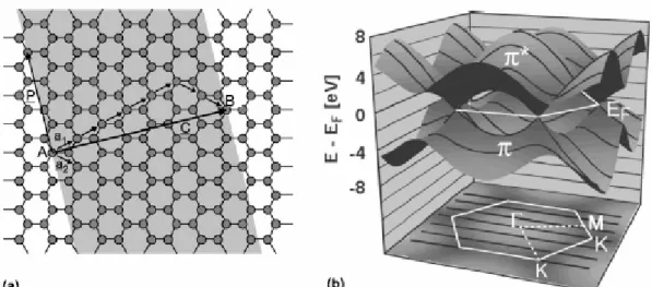
nanotube depend on the direction in which the sheet was rolled up, as shown as Fig. 2-6
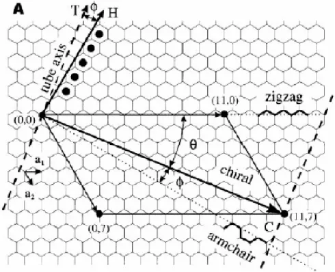
[16]. A CNT of the chiral vector is defined on the hexagonal lattice as Ch = nâ1 + mâ2,
where â1 and â2 are unit vectors, and n and m are integers. The chiral angle, q, is
measured relative to the direction defined by â1. This diagram has been constructed for
(n, m) = (4, 2), and the unit cell of this nanotube is bounded by OAB'B. To form the
two ends are capped with half of a fullerene molecule. Different types of CNTs have
different values of n and m. (b) Zigzag nanotubes correspond to (n, 0) or (0, m) and have
a chiral angle of 0°, armchair nanotubes have (n, n) and a chiral angle of 30°, while
chiral nanotubes have general (n, m) values and a chiral angle of between 0° and 30°, as
shown as Fig. 2-7 [17]. According the theory, nanotubes can either be metallic or
semiconducting. Some nanotubes are metals with high electrical conductivity, while
others are semiconductors. Nanotubes also have remarkable mechanical properties [18]
that can be exploited to strengthen materials or to act as "tips" in scanning probe
microscopes, as shown as Fig. 2-8 [19]. And since they are composed entirely of CNTs
also have a low specific weight. MWNTs are close to hollow graphite fibers, except that
they have a much higher degree of structural perfection. The interlayer spacing in
MWNT (d(002) = 0.34 nm) is slightly larger than that in single crystal graphite (d(002) =
0.335 nm). This is attributed to a combination of tubule curvature and van der Waals
force interactions between successive graphene layers. The single-walled nanotubes
(SWNTs) and possess good uniformity in diameter about 1.2 nm. They are close to
fullerenes in size and have a single-layer cylinder extending from end to end. Qin et al.
also reported that high-resolution transmission electron micrograph of an 18-shell CNT
nanotube is shown by the reduced contrast towards the centre of the nanotube, where
there are fewer atoms in the smaller tubes, as shown as Fig. 2-9 [20].
Carbon is the elemental equivalent of the perfect neighbor, friendly, and easygoing,
as shown as Fig. 2-10 [21]. Under intense pressure, carbon atoms form co-valence
bonds with four neighbor atoms, creating the pyramidal arrangement of diamond.
However, the activation energy of diamond is very high and carbon usually links up
with just three neighbors, creating the hexagonal rings of graphite network.
The arrangement of graphite has a host of unpaired electrons, which essentially
float above or below the plane of carbon rings. In this arrangement, the electrons have
more freedom to move around the graphite surface, which makes the material a good
electrical conductor. S. Paulson et al. reported that junction resistance between a CNT
and a graphite substrate and show that details of momentum conservation also can
change the contact resistance, as shown as Fig. 2-11 and Fig. 2-12 [22].
CNTs consist of concentric hexagon-rich cylinders, made up of sp2 hybridized
carbon, as in graphite, and terminated by end-caps arising from the presence of 12
pentagons (six per end). It is possible to construct a cylinder by rolling up a hexagonal
graphene sheet in different ways. Two of these are “non-helical” in the sense that the
named “armchair” and “zig-zag”. In the armchair structure, two C-C bonds on opposite
sites of each hexagon are perpendicular to the tube axis, whereas in the zig-zag
arrangement, these bonds are parallel to the tube axis. In all other conformation, the C-C
bonds lie at an angle to the tube axis and a helical structure is obtained [15].
Theoretical calculations have predicted that all the armchair tubes are metallic
whereas the zig-zag and helical tubes are either metallic or semiconducting. The
electronic conduction process in nanotubes is unique since in the radial direction, the
electrons are confined in the singular plane of the graphene sheet. The conduction
occurs in the armchair (metallic) tubes through gapless modes as the valence and
conduction bands cross each other at the Fermi energy, as shown as Fig. 2-13[23]. In
most helical tubes, which contain large numbers of atoms in their unit cell, the
one-dimensional band structure shows an opening of the gap at the Fermi energy, and
this leads to semiconducting properties. This unique electronic behavior only occurs for
small nanotubes. As the diameter of the tubes increases, the band gap (which varies
inversely with the tube diameter) tends to zero, yielding a zero-gap semiconductor that
is electronically equivalent to the planar graphene sheet. In a SWNT, the outer planar
graphene-like tubes superimpose the electronic structure of the inner tubes. The band
structure obtained from individual SWNT resembles that of graphite. Experiments have
introducing sharp resonance in the local density of states, as shown as Fig. 2-14[24].
2.3 Characteristics of carbon nanotube
2.3.1 Mechanical properties
In a sheet of graphite each carbon atom is strongly bonded to three other atoms,
which makes graphite very strong in certain directions. However, adjacent sheets are
only weakly bound by van der Waals forces, so layers of graphite can be easily peeled
apart - as happens when writing with a pencil. As we shall see, it is not so easy to peel a
carbon layer from a multiwall CNTs. Carbon fiber is already used to strengthen a wide
range of materials. A simple method was used to assemble single-walled CNTs into
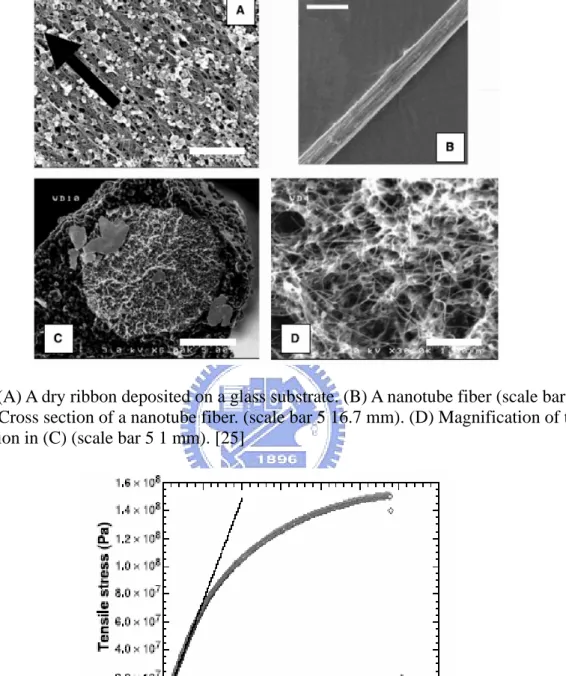
indefinitely long ribbons and fibers, as shown as Fig. 2-15[25]. The processing consists
of dispersing the nanotubes in surfactant solutions, recondensing the nanotubes in the
flow of a polymer solution to form a nanotube mesh, and then collating this mesh to a
nanotube fiber, as shown as Fig. 2-16[25].
The special properties of CNTs mean that they could be the ultimate high-strength
measured the Young's modulus of CNTs. The Young's modulus of a material is a
measure of its elastic strength. Yu et al. reported that the tensile strengths of individual
microscope, as shown as Fig. 2-17[26]. The tensile-loading experiment was prepared
and observed entirely within the microscope and was recorded on video. Analysis of the
stress-strain curves for individual MWCNTs indicated that the Young's modulus E of the
outermost layer varied from 270 to 950 gigapascals, as shown as Fig. 2-18[26].
It is now known that the Young's modulus should approach a value of 1.25
terapascals. This is true both for multiwall and single-wall CNTs because the modulus is
mainly determined by the carbon-carbon bonds within the individual layers.
The bending stiffness can also be measured by placing the nanotubes across probe
and using an atomic force microscope to bend them in the middle. Wong et al. reported
that atomic force microscopy was used to determine the mechanical properties of
individual, structurally isolated silicon carbide (SiC) nanorods (NRs) and CNTs that
were pinned at one end to molybdenum disulfide surfaces. The bending force was
measured versus displacement along the unpinned lengths, as shown as Fig. 2-19 [27].
The CNTs were about two times as stiff as the SiC NRs. Continued bending of the SiC
NRs ultimately led to fracture, whereas the MWNTs exhibited an interesting elastic
buckling process. The strengths of the SiC NRs were substantially greater than those
found previously for larger SiC structures, and they approach theoretical values.
of the SiC NRs, although the MWNTs represent a uniquely tough, energy-absorbing
material, as shown as Fig. 2-20 [27]. The Young’s modulus, strength, and toughness of
nanostructures are important to proposed applications ranging from nanocomposites to
probe microscopy.
Occasionally a nanotube spanned one of the pores and the microscope was used to
measure how the deflection, which is inversely proportional to the Young's modulus,
varied with the applied force. Tombler et al. show that the effects of mechanical
deformation on the electrical properties of CNTs are of interest given the practical
potential of nanotubes in electromechanical devices. He reports an experimental and
theoretical elucidation of the electromechanical characteristics of individual SWNTs
under local-probe manipulation. Use AFM tips to detect suspended SWNTs reversibly,
without changing the contact resistance; in situ electrical measurements reveal that the
conductance of an SWNT sample can be reduced by two orders of magnitude when
deformed by an AFM tip. The tight-binding simulations indicate that this effect is owing
to the formation of local sp3 bonds caused by the mechanical pushing action of the tip,
as shown as Fig. 2-21 and Fig. 2-22 [28]. One recent experiment used the tip of an AFM
to manipulate CNTs, revealing that changes in the sample resistance were small unless
nanotubes.
CNTs are different: first they will bend over to surprisingly large angles, before
they start to ripple and buckle, and then finally develop kinks as well. The amazing
thing about CNTs is that these deformations are elastic - they all disappear completely
when the load is removed.
2.3.2 Electronic properties
CNTs are giant molecular wires in which electrons can propagate freely, just as
they do in an ordinary metal. This contrasts strongly with conventional "conducting" in
which the electrons are localized. These molecules are actually insulators and only
become conductors if they are heavily doped, as shown as Fig. 2-23 [29]. CNTs can be
doped either by electron donors or electron acceptors. After reaction with host materials,
the dopants are intercalated in the intershell spaces of the CNTs, and in the case of
single-walled nanotubes either in between the individual tubes or inside the tubes, as
shown as Fig. 2-24 [29]. The reaction of intercalation can be carried out in the vapour or
Graphite, on the other hand, can conduct electricity because one of the four valence
electrons associated with each carbon atom is delocalized and can therefore be shared
by all the carbon atoms. However, it turns out that a single sheet of graphite (also
known as graphene) is an electronic hybrid. Although not an insulator, it is not a
semiconductor or a metal either. Graphene is a "semimetal" or a "zero-gap"
semiconductor. This peculiarity means that the electronic states of graphene are very
sensitive to additional boundary conditions, such as those imposed by rolling the
graphene into a tube. A CNT can be thought of as being formed by folding a piece of
graphene to give a seamless cylinder. The description of this process in terms of the
chirality vector and the naming of nanotubes are given in Fig. 2-25(a) [30]. The
interesting electrical properties of CNTs are due in a large part to the peculiar electronic
structure of the graphene. Its band-structure (E vs. k relation) and the hexagonal shape
of its first Brillouin zone are shown in Fig. 2-25(b) [30].
It can be shown that a stationary electron wave can only develop if the
circumference of the nanotube is a multiple of the electron wavelength. This boundary
condition means that a nanotube is either a true metal or a semiconductor - a fact that
has been confirmed in experiments with single-wall nanotubes.
energy is not high enough to excite optical phonons. When these vibrational modes
become excited the resulting energy dissipation eventually leads to the breakdown of
the CNT structure. Since in defect-free CNTs transport is ballistic, high-energy carriers
can be formed by hot carrier injection at the contacts. Thus, the stability of a CNT
depends on the nature of the contacts. Another factor that influences the stability of a
CNT is the gaseous environment it is in. Experiments have shown that the threshold
power that is needed to induce breakdown in a CNT is drastically lower in air than it is
in vacuum. Particularly interesting is the breakdown behavior of MWCNTs. Fig. 2-26
[30] shows the variation with time of the current flowing through a MWCNT under a
bias leading to breakdown. A very regular current staircase is clearly seen.
One would expect to find more complex behavior for CNTs because of interactions
between adjacent layers, and this is the subject of ongoing research. Moreover, by
combining different nanotubes, and supplementing them with gate electrodes, there is
the potential to make a wide variety of electronic devices, ranging from quantum wires
to field effect transistors.
On the fundamental side, a perfect metallic nanotube should be a ballistic
conductor. In other words, every electron injected into the nanotube at one end should
resistance is independent of its length, which means that Ohm's law does not apply.
Indeed, only a superconductor (which has no electrical resistance whatsoever) is a better
conductor. Any wave that hits two semireflective barriers, one after the other, will
produce an interference pattern. This pattern consists of regular oscillations in the
intensity of the transmitted wave across the double barrier, as a function of wavelength.
Liang et al. report such oscillations in the transmission of electrons through a metallic
SWNT hundreds of nanometres long that is held between two electrodes, as shown as
Fig. 2-27 [31]. This experiment demonstrates the quantum-mechanical wave nature of
electrons. It also shows that the propagation of electrons in the nanotube is
ballistic-largely free from scattering-over distances of thousands of atoms. A few years
ago, we predicted theoretically the possibility of ballistic propagation of electrons over
such distances in metallic SWNTs. The creation by Liang et al. of a device that relies on
this effect for its operation confirms this and other results that indicate ballistic transport
through metallic CNTs, and is a stunning achievement.
2-3-3. Quantized conductance
This method for making electrical contact with nanotubes is very different to
only be observed if ideal contacts are made to the nanotube, and these can be very
difficult to achieve. (In an ideal contact none of the electrons entering or leaving the
nanotube will be backscattered by the contact.) Early experiments with microfabricated
contacts found strong evidence that electrons were scattered. The transport therefore
appeared to be diffusive rather than ballistic. Limiting the length of a CNT leads to a
“particle-in-a-box” quantization of the energy levels. Such discrete energy levels have
been observed in transport experiments on individual nanotubes and ropes. The electron
wave functions corresponding to these discrete states can in principle be imaged by
scanning tunneling microscopy (STM). The well-known STM work on quantum corrals
demonstrated that wave patterns could be directly imaged in the local density of states
of a 2D metal surface, as shown as Fig. 2-28 [32]. The wave functions of several
adjacent energy levels can be displayed simultaneously by plotting the differential
conductance dI/dV as a function of the voltage and the position x along the tube (Fig.
3A). Wave patterns can be observed for four different energy levels appearing at bias
voltages of 0.11, 0.04, 0.00, and –0.05 V (15), as shown as Fig. 2-29 [32]. At each level,
a horizontal row of about seven maxima is resolved in dI/dV as a function of position x
along the tube (see Fig. 2-28 for the 1D spatial profile of the wave functions belonging
2.3.4 Thermal properties
Many phenomena in nature occur as the result of some kind of imbalance. For
instance, heat is transported when there is a temperature gradient between two
boundaries of a material. Despite their ubiquity in everyday life, many aspects of such
phenomena are still the subject of debate among theoretical physicists. One central issue
is the role of spatial constraints, caused by the dimensionality of a system: the response
of a system to external forces is intimately related to statistical fluctuations within it,
and these, in turn, depend strongly on whether the system is one-, two or
three-dimensional. Because of the variety and complexity of specific interactions,
simplified microscopic models are an invaluable tool for the study of transport
mechanisms in reduced dimensions, as shown as Fig. 2-30 [33]. The old problem of
heat conduction on the thermal conductivity should increase with the system size. In
other words, the larger the system, the more efficiently heat is transported (assuming
that the density of the material and the temperature gradient are fixed)-in physical terms,
the mean free path of the ‘heat carriers’increases with the length of the sample.
A system of fewer than three dimensions-confirming that space dimensionality is
crucial in anomalous transport properties. More specifically, the thermal conductivity
with exponent 1/3; for a two-dimensional system, the divergence is much weaker and
logarithmic. But such anomalous behaviour disappears in three dimensions. Transport
anomalies such as this have been found in many microscopic models, including
one-dimensional crystals. Although it may seem strange to consider a one-dimensional
crystal as a fluid, it is nonetheless well known that mechanical vibrations in a crystal
structure can be described by hydrodynamic equations similar to those used in a fluid,
as interacting phonons in a crystal behave similarly to particles in a fluid.can the
anomalous behaviour actually be described by universal scaling laws, and to what
extent does it depend on the nature of the microscopic interactions? The conceptual
challenge is not the only reason for studying energy transport in spatially constrained
systems-there is also a variety of real systems in which these anomalies are important.
SWNTs (Fig. 2-30 [33]) are known through experiment to have an unusually high
thermal conductivity, which is attributed mainly to quasi-one-dimensional lattice
vibrations, and it is reasonable to expect that the scaling laws derived for simple models
should apply to nanotubes as well. Although, so far, an experimental test is lacking,
molecular-dynamics simulations that use realistic energy potentials for the carbon atoms
support this idea. If the thermal conductivity did increase with nanotube length in a
well-defined way, this would be a very promising feature to use in technological
nanocircuits. In building models of energy-transport processes, the aim is to single out
generic physical features, although this might sometimes be at the price of drastic
simplifications. Hopefully, in the end the results will go beyond pure academic interest
and suggest new ideas for technological applications-perhaps the reader is astonished
that so many interesting and innovative ideas are still emerging from classical
mechanics [33].
2.3.5 Magnetic fields properties
Nanotubes have also been used to help demonstrate the Aharonov-Bohm effect,
one of the most fundamental phenomena in quantum physics. In the Aharonov-Bohm
effect a beam of quantum particles, such as electrons, is split into two partial beams that
pass on either side of a region containing a magnetic field, and these partial beams are
then recombined to form an interference pattern. The interference pattern can be altered
by changing the magnetic field-even though the electrons do not come into contact with
the magnetic field, as shown as Fig. 2-31 [34].
The small diameter of CNTs is very favorable for field emission - the process by
which a device emits electrons when an electric field or voltage is applied to it. Field
emission is important in several areas of industry, including lighting and displays, and
the relatively low voltages needed for field emission in nanotubes could be an
advantage in many applications. However, as with all new technologies, there are
formidable obstacles to be overcome. CNTs can act as electron sources with very rigid
structures, making them particularly interesting for use as point electron sources in
high-resolution electron-beam instruments, as shown as Fig. 2-32 [35].
Two parameters of an electron source affect the resolution of these instruments: the
energy spread of the emitted electrons and a parameter called the reduced brightness,
which depends on the angular current density and the virtual source size. To measure the
reduced brightness, and find a value that is more than a factor of ten larger than
provided by state-of-the-art electron sources in electron microscopes. In addition, an
individual CNT emits most current into a single narrow beam, as shown as Fig. 2-33
[35].
On the basis of these results, we expect that CNT electron sources will lead to a
significant improvement in the performance of high-resolution electron-beam
2.3.7 Biology and nanotube
Since the discovery of their one dimensional electronic band structure, the leading
candidate that has emerged for nanodevice applications is SWNTs. Their unique
properties with the specific molecular-recognition features of DNA by coupling SWNTs
to peptide nucleic acid (PNA, an uncharged DNA analogue) and hybridizing these
macromolecular wires with complementary DNA. The findings provide a new, versatile
means of incorporating SWNTs into larger electronic devices by recognition-based
assembly, and of using SWNTs as probes in biological systems by sequence-specific
attachment, as shown as Fig. 2-35 [36]. The recognition properties imparted to SWNTs
by oligonucleotide adducts could be used to programme the attachment of SWNTs to
each other and to substrate features, such as electrodes, on which monolayers of
complementary sequences are self-assembled. The antisense properties of PNA–SWNTs
might also be exploited in a biological context, for example in biosensors.
2.4.1 Arc-discharge methods
The observed nanotubes synthesized from the electric-arc discharge technique.
Shown schematically in Fig. 2-36 [37], the arc discharge technique generally involves
the use of two high-purity graphite rods as the anode and cathode. The rods are brought
together under a helium atmosphere and a voltage is applied until a stable arc is
achieved. The exact process variables depend on the size of the graphite rods. As the
anode is consumed, a constant gap between the anode and cathode is maintained by
adjusting the position of the anode. The material then deposits on the cathode to form a
build-up consisting of an outside shell of fused material and a softer fibrous core
containing nanotubes and other carbon particles. To achieve single walled nanotubes,
the electrodes are doped with a small amount of metallic catalyst particles.
2.4.2 Laser vaporization
Laser ablation was first used for the initial synthesis of fullerenes. Over the years,
the technique has been improved to allow the production of SWNTs. In this technique, a
laser is used to vaporize a graphite target held in a controlled atmosphere oven at temperatures near 1200 °C. The general set-up for laser ablation is shown in Fig. 2-37
[37]. To produce SWNTs, the graphite target was doped with cobalt and nickel catalyst.
arc-discharge and the laser-ablation techniques are limited in the volume of sample they
can produce in relation to the size of the carbon source (the anode in arc-discharge and
the target in laser ablation). In addition, subsequent purification steps are necessary to
separate the tubes from undesirable by-products.
2.4.3 Chemical vapor deposition
Since separation of CNTs is difficult and the yield is low, they are very expensive.
However, the catalytic CVD technique, which employs the catalytic decomposition of
short-chain hydrocarbons, can produce relatively large amounts of CNTs under mild
conditions. Moreover, this process makes it possible to control the size and growth
density of CNTs by dispersing the catalyst particles on supports and adjusting the
reaction parameters at relatively lower temperatures in comparison with the former
processes. These limitations have motivated the development of gas-phase techniques,
such as Thermal Chemical Vapor Deposition (Thermal CVD), as shown as Fig. 2-38
[38], where nanotubes are formed by the decomposition of a carbon-containing gas. The
gas-phase techniques are amenable to continuous processes since the carbon source is
continually replaced by flowing gas. In addition, the final purity of the as-produced
2.5 The mechanism of carbon nanotubes growth
2.5.1 The diffusion path of carbons atom
A typical growth condition may involve the following step in Fig. 2-39 [39].
(1) Hydrocarbon dissociate and deposit carbon on surface.
(2) Carbon diffuses through solid metal.
(3) Carbon precipitates as curved graphitic layers.
2.5.2 Tip growth mode and base growth (root growth) mode
Based on the position of metal particle on the tube, there were two kinds of growth
mode: one is called “base-growth” and the other is called “tip-growth”. The
“base-growth” mode meant that the tube grew upward from metal particles, which
attached to the substrate. If the metal particle detached and moved to the head of the
Fig. 2-1 Perspective view of a rope of (10,10) carbon nanotubes. [12]
(a) (b)
Fig. 2-2 Atomic structure and spectroscopy of metallic SWNTs. STM images of a SWNT [13]
(a) (b) (b)
Fig. 2-4 (a) armchair, zigzag, and chiral SWNTs. (b) Tunneling electron microscope image of a 1.3-nm-diameter chiral SWNT. (c) Transmission electron microscope (TEM) image of a MWNT [15]
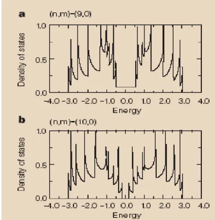
Fig. 2-6 Calculated one-dimensional electronic density of states on single-wall nanotubes. [16]
Fig. 2-7 Relation between the hexagonal carbon lattice and the chirality of carbon nanotubes. [17]
(a) (b)
(c) (d)
Fig. 2-8 (a) Characterization of CVD nanotube tips. (b) Transmission electron microscope (TEM) image of a CVD nanotube tip. (c) Tip oscillation amplitude (d) Imaging IgM macromolecules with a CVD nanotube tip at high resolution. [19]
Fig. 2-9 High-resolution electron microscope image of a 4 Å tubule (side walls are marked by lines) confined inside an 18-shell carbon nanotube. [20]
Fig. 2-10 Diamond and Graphite structures [21]
Fig. 2-11 (A) A conducting AFM tip is used to measure the resistance of the NT-HOPG interface. (B) The NT is in registry. (C) The NT Fermi-level states (dotted arrow) [22]
Fig. 2-12 (A) A tube that has been rotated through 180¡. (B) More dense data over one period on a different tube gives us a better indication of the shape of the curve. [22]
Fig. 2-13 In a metallic carbon nanotube, left-moving electrons (red) and right-moving electrons (blue) belong to two different bands with distinct microscopic structures. [23]
Fig. 2-14 (A) Typical atomically resolved STM image of a (15,0) SWNT. Scale bar, 1 nm. (B) Tunneling conductance data (C) Typical high-resolution normalized conductance (dI/dV)/(I/V) curves and measured I-V curves [24]
Fig. 2-15 (A) A dry ribbon deposited on a glass substrate. (B) A nanotube fiber (scale bar 5 25 mm). (C) Cross section of a nanotube fiber. (scale bar 5 16.7 mm). (D) Magnification of the bright region in (C) (scale bar 5 1 mm). [25]
Fig. 2-16 Mechanical measurements under tensile loading performed at a strain rate of 1% per minute.. [25]
Fig. 2-17 (A) An SEM image of two AFM tips holding a MWCNT.(B) High-magnification SEM image of the indicated region in (A), showing the MWCNT between the AFM tips. (C) Higher magnification SEM image [26]
Fig. 2-18 (A) Schematic showing the principle of the tensile-loading experiment. (B) Plot of stress versus strain curves for individual MWCNTs. [26]
Fig. 2-19 (A) SiC NRs or carbon nanotubes (B) Optical micrograph of a sample showing the SiO pads (white) and the MoS2 substrate (blue).. (C) An AFM image of a 35.3-nm-diameter SiC NR (D) Schematic of beam bending with an AFM tip. The tip (blue triangle) [27]
Fig. 2-20 (A)Surface plot showing the F-d responseof a 23.0-nm-diameter SiC NR (B) Dependence of the force constant k(x) on position x along the axis of the same NR [27].
Fig. 2-21. a. Device viewed from above. Preparation of samples involves chemical vapour deposition of SWNTs b, AFM image of an SWNT c. Side-view of the AFM pushing
Fig. 2-22 a. Experimental result of conductance. b. Conductance versus band energy calculated for an ideally contacted (5,5) SWNT. c,d. Simulated atomic configurations of the
Fig. 2-23 CESR (conduction electron spin resonance) of SWNT bucky paper films electrochemically doped by K for K C various x compositions. [29]
Fig. 2-24 Schematic of three types of MWNT (a) intershell intercalation; (b) no reaction; (c) intercalation-assisted break-up. [29]
Fig. 2-25 (a) Schematic illustration of the generation of a nanotube (b)Top: Band-structure of the 2D graphene sheet (in gray). [30]
Fig. 2-26 Time-dependence of the current flowing through a multi-walled nanotube during current-induced breakdown. [30]
Fig. 2-28 (A) Example of a nanotube (B) Atomically resolved image of an armchair nanotube. [32]
Fig. 2-29 (A) I-V characteristics of the tube. (B) Differential conductance dI/dV versus V, as calculated from the I-V curves. (C) Differential conductance dI/dV as a function of position along the tube. [32]
Fig. 2-30 Simple models and real materials. [33]
(a) (b)
Fig. 2-32 TEM images of an individual multi-walled carbon nanotube b, High-resolution TEM image of the apex of the tube.[35]
Fig. 2-33 a. Schematic overview of the point projection microscope. b. The Fresnel interference pattern of a hole in a thin carbon film [35]
Fig. 2-34 The emission pattern on a phosphor screen of an electron source consisting of an individual multi-walled carbon nanotube. [35]
Fig. 2-35 a, b, N-hydroxysuccinimide (NHS) esters formed on carboxylated. d, e, Atomic-force microscope (Tapping Mode) images of PNA–SWNTs. [36]
Fig. 2-39 Scheme with some parameters involved in the reaction kinetics of the growth mechanism of CNTs. [39]
Fig. 2-40 Schematics of tip-growth and extrusion mechanisms for carbon filament growth after Baker and Harris. [40]
![Fig. 2-2 Atomic structure and spectroscopy of metallic SWNTs. STM images of a SWNT [13]](https://thumb-ap.123doks.com/thumbv2/9libinfo/8754717.206626/43.892.110.787.549.924/fig-atomic-structure-spectroscopy-metallic-swnts-images-swnt.webp)
![Fig. 2-3 HRTEM image of two nanotubes with outer diameters of 6 nm and 16 nm. [14]](https://thumb-ap.123doks.com/thumbv2/9libinfo/8754717.206626/44.892.247.650.445.881/fig-hrtem-image-nanotubes-outer-diameters-nm-nm.webp)
![Fig. 2-10 Diamond and Graphite structures [21]](https://thumb-ap.123doks.com/thumbv2/9libinfo/8754717.206626/50.892.156.743.228.820/fig-diamond-graphite-structures.webp)
![Fig. 2-31 Observing the Aharonov–Bohm effect.[34]](https://thumb-ap.123doks.com/thumbv2/9libinfo/8754717.206626/65.892.266.628.233.518/fig-observing-the-aharonov-bohm-effect.webp)
![Fig. 2-33 a. Schematic overview of the point projection microscope. b. The Fresnel interference pattern of a hole in a thin carbon film [35]](https://thumb-ap.123doks.com/thumbv2/9libinfo/8754717.206626/66.892.236.664.528.823/schematic-overview-projection-microscope-fresnel-interference-pattern-carbon.webp)
