國
立
交
通
大
學
電子工程系 電子研究所
碩
士
論
文
金屬奈米點記憶特性及研究
The memory characterization and investigation of metal
nanocrystal
研 究 生:陳 德 安
De-An Chan
指導教授:羅 正 忠 博士
Dr. Jen-Chung Lou
金屬奈米點記憶特性及研究
The memory characterization and investigation of metal
nanocrystal
研 究 生:陳德安 Student:De-An Chan
指導教授:羅正忠 博士 Advisor:Dr. Jen-Chung Lou
邱碧秀 博士 Dr. Bi-shiou Chiou
國 立 交 通 大 學
電子工程學系 電子研究所
碩 士 論 文
A Thesis Submitted toDepartment of Electronics Engineering & Institute of Electronics College of Electrical and Computer Engineering
National Chiao Tung Unicersity in Partial Fulfillment of the Requirements
For the Degree of Master In
Electronic Engineering June 2007
Hsinchu, Taiwan, Republic of China
金屬奈米點記憶特性及研究
研究生:陳德安 指導教授:羅正忠 博士
邱碧秀 博士
國立交通大學
電子工程學系 電子研究所
摘要
早期非揮發性記憶體的製作,是採用整層的複晶矽的浮停閘(Floating Gate)結 構,利用此層來當電子的儲存層,當電子由通道注入到這層浮停閘之後,會影響 到元件的臨界電壓值(Threshold voltage),藉由判別臨界電壓的電壓值大小,即可 定以邏輯的 “0” & “1” 狀態。但是,因為這種浮停閘結構為整層的半導體薄膜, 在電子反覆的從穿遂氧化層進出這層浮停閘,會使得穿遂氧化層裂化以至於出現 缺陷,當缺陷一產生之後,所有儲存的電子將會隨這這層缺陷而有了漏電路徑, 導致所寫入的電子全部流失掉,無法達到記憶的效果。然而在不久的將來,會因MRAM 等…… 而在這個過渡時期,如何利用現有的技術,帶領快閃記憶體(Flash Memory) 在繼續的走過下一個世代。許多研究論文提出了利用半導體或金屬的奈米點來當 作電子的儲存層。利用奈米點的好處是,各個奈米點之前被絕緣體所包圍,所以 當穿遂氧化層產生缺陷後,電子不會全部流失掉,僅僅流失掉缺陷附近儲存的電 子,所以可以進一步應付尺寸的微縮和增加電子的保存能力(retention)。降低穿遂 氧化層厚度,使得可以減少操作電壓,增加電子寫入的效率。此外,利用金屬奈 米點電晶體還有幾個好處,一個是他能擁有高的狀態密度,再來就是金屬較半導 體有著更大的功函數,當電子注入到金屬奈米點之中後是儲存在較深層的能階 中,它所看到的能障較高,不易因鄰近元件的操作造成擾動,預期也能提升電子 的保存時間。再來,因為各個奈米點注入了電子後,會因為庫倫阻絕(Coulomb blockade)效應,所儲存的電子會排斥後續電子的寫入。故在低電壓操作模式下(例 如讀取時),電子不易被寫入到奈米點內,也就是有比較少的讀取干擾,在辨別邏 輯 “0” & “1” 上會較為容易。
The memory characterization and investigation of metal
nanocrystal
Student:De-An Chan Advisor:Dr. Jen-Chung Lou
Dr. Bi-shiou Chiou
Department of Electronics Engineering & Institute of Electronics
College of Electrical and Computer Engineering
National Chiao-Tung University
ABSTRACT
In early time, manufacture the nonvolatile memory uses poly-silicon layer treated as electron storage layer named floating gate(FG). When electron inject to this layer from channel. That will be influence the threshold voltage. Two state threshold voltages constitute logic “0” & “1”. For FG structure, the oxide has a defect because of
layer made by semi-conduct or metal nano-crystal. The benefit is that nano-crystal surrounded by dielectric. When oxide has defect merely lose the electron which nearby the defect stores up. So nano-crystal device can maintain good retention characteristics. Therefore may further deal with the aggressive size scale down, reduce tunneling oxide thickness, may reduce the operation voltage, the efficiency which the increase electron writes in. Otherwise metal nano-crystal has higher density of states, and the design freedom of engineering the work functions to optimize device characteristics. Coulomb blockade effect can effectively inhibit electron tunneling at low gate voltage and improve the flash memory array immunity to read disturbance, can easy recognize logic “0” & “1”.
誌 謝
首先,我要感謝我的指導教授羅正忠博士和邱碧秀博士,在我就讀碩 士班的這兩年來,給予熱心的協助與指導,對學生們的生活細節及處世態 度也循循善誘,兩年來領受到許多不同方面的啟發與指導。 其次我要感謝的是林柏村博士、陳永裕博士,對於我們實驗上所遇到 的問題,給予熱心的指導與建議。還有同學大峰、信智、正凱、智仁、宏 仁、建宏、昱鈞、建彰、俐婷、睿龍以及勝凱在生活上及學業方面彼此切 磋鼓勵和實驗上的幫助,甚至在假日時還熱心的幫忙指導儀器操作。還有 學弟佳樺、信富、國洲、元愷、晨修、嘉宏等學弟對我於實驗上的幫忙及 畢業論文的貢獻,感謝學弟們讓實驗室在嚴肅的研究氣氛中增添了許多歡 樂。同時感謝我大學同學及室友,常常陪伴我一同吃宵夜聊天排解我郁悶 的心情。 最後,感謝父母親陳永水先生及王淑玉女士,在這24 年來無為不至的 關懷照顧及支持還有感謝我的哥哥陳家仲及妹妹陳家羚在精神上的支持, 再這樣一個美好的家庭裡,我得以全力以赴完成學業及研究。Contents
Chapter 1 Introduction... 1
1.1 General Background ... 1
1.2 Organization of this thesis ... 3
Chapter 2 Nonvolatile memory basic concept and operation mechanism... 8
2.1 Introduce ... 8
2.1.1 SONOS nonvolatile memory devices... 8
2.1.2 Nanocrystal nonvolatile memory devices... 9
2.2 Memory basic concept ... 13
2.2.1 Reading operation ... 13
2.2.2 Write/Erase operation mechanism ... 13
2.2.2.1 Channel Hot-Electron Injection (CHEI)... 14
2.2.2.2 F-N tunneling... 15
2.2.2.3 Direct Tunneling ... 16
2.2.3 Data retention ... 16
2.2.4 Endurance... 17
Chapter 3 Metal nanocrystal memory use Co nanodot ... 24
3.1 Motivation... 24
3.3 Result and discussion ... 25
3.3.1 Self-Assembled Nanocrystal Formation... 25
3.3.2 Memory characteristics ... 27
3.3.3 Programming/Erase characteristics ... 28
3.3.4 Data retention characteristics ... 28
3.4 Summay... 29
Chapter 4 Conclusions and recommendations for future works ... 44
4.1 Conclusion... 44
4.2 Recommendation for future works... 44
List of Figures
Chapter 1
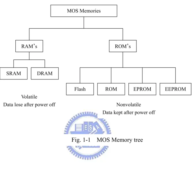
Fig. 1-1 MOS Memory tree
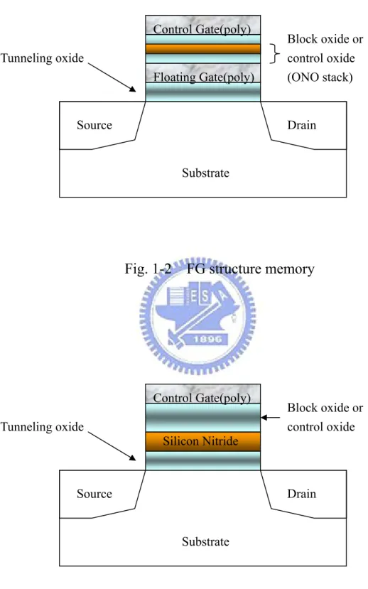
Fig. 1-2 FG structure memory
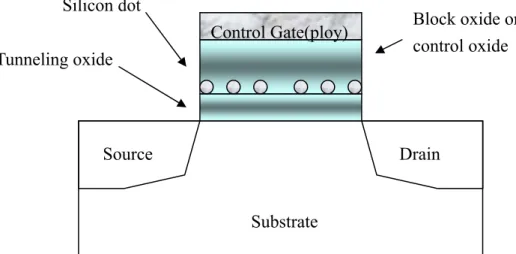
Fig. 1-3 SONOS structure memory
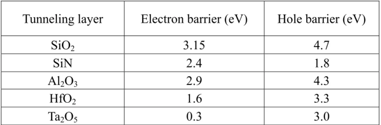
Fig. 1-4 Nanocrystal structure memory
Chapter 2
Fig. 2-1 SONOS band diagram during retention mode
Fig. 2-2 FG band diagram during retention mode
Fig. 2-3 Memory reading operation
Fig. 2-4 Memory band diagram in (a)write mode (b)Erase
mode
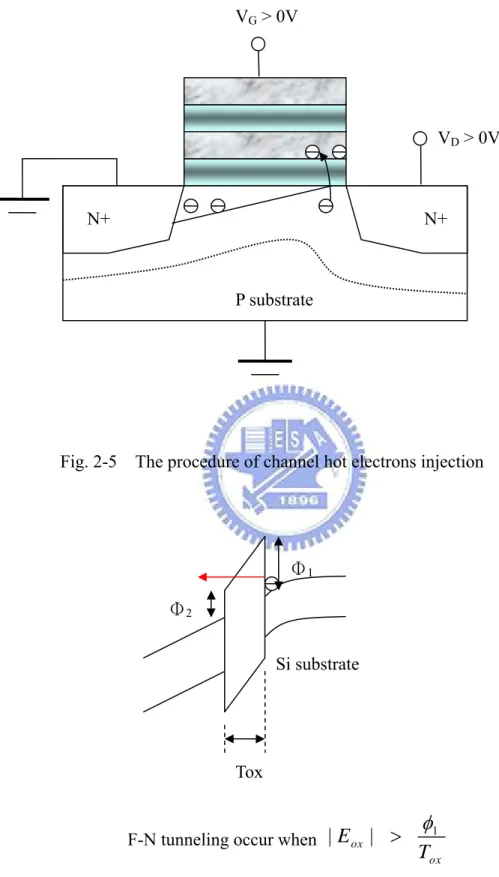
Fig. 2-5 The procedure of channel hot electrons injection
Fig. 2-6 The procedure of F-N tunneling
Chapter 3
Fig. 3-1 2-bit memory device
Fig. 3-2 process flowchart
Fig. 3-3 Co RTA 600℃ 60s sample AFM pictcure
Fig. 3-4 Co RTA 700℃ 30s sample AFM pictcure
Fig. 3-5 Co RTA 700℃ 60s sample AFM pictcure
Fig. 3-6 Co RTA 800℃ 30s sample AFM pictcure
Fig. 3-7 Co RTA 900℃ 30s sample AFM pictcure
Fig. 3-8 RTO samples C-V curve
Fig. 3-9 RTA 700℃ 30s sample C-V curve
Fig. 3-10 RTA 700℃ 60s sample C-V curve
Fig. 3-11 RTA 800℃ 30s sample C-V curve
Fig. 3-12 RTA 900℃ 30s sample C-V curve
Fig. 3-13 RTA 700℃ 60s sample program speed
Fig. 3-14 RTA 700℃ 60s sample erase speed
Fig. 3-15 RTA 700℃ 60s sample data retention
Fig. 3-16 RTA 700℃ 60s sample leakage current
Fig. 3-17 RTA 800℃ 30s sample program speed
Fig. 3-18 RTA 800℃ 30s sample erase speed
Fig. 3-19 RTA 800℃ 30s sample data retention
Fig. 3-20 RTA 800℃ 30s sample leakage current
List of Tables
Chapter 2
Table 2-1 Electron and hole barrier high for SiO
2and Si
3N
4Chapter 3
Table 3-1 Some character about cobalt
Table 3-2 Experiment split table
Chapter 1
Introduction
1.1 General Background
Since 1960 ages, the first semiconductor transistor is invented. One of great invention is semiconductor memory, semiconductor memory market is expected will have great increase. These memories approximately divide into two categories: random access memories (RAM’s) and read-only memory (ROM’s). See Fig. 1-1. These two kinds of memories most different in data retention. Data will be reserved or said nonvolatile after power off named ROM, opposite one data will be lost or said volatile after power off named RAM. The volatile memories like SRAM or DRAM, that very dense and have fast speed in writing and reading. RAM is massive applied in computer industry. The nonvolatile memories like EPROM, EEPROM, or Flash, are able to balance the less-aggressive programming and reading performances with no volatility.
In 1967, D. Kahng and S. M. Sze invented the first floating-gate nonvolatile semiconductor memory at Bell Labs [1.1]. The FG structure device show in Fig. 1-2. It has a poly-silicon gate completely surrounded by dielectric. The floating gate is electrically governed by a capacitive couple control gate (CG). When electrons injected to the floating gate from channel, electrons in the floating gate will influence device threshold voltage, use the threshold voltage difference to recognize logic “0” & “1”. Several physical mechanisms are available to accomplish this charge transfer, but the most commonly used ones are either channel hot electron injection (CHEI) or Fowler-Nordheim (FN) tunneling for the write operation, and FN tunneling for the erase operation.
The stacked-gate FG device structure continues to be the most prevailing nonvolatile semiconductor memory(NVSM) implementation, and is widely used in both standalone and embedded memories, and in both code and data storage applications. Although convention FG memories have many advantages over other kinds of nonvolatile memories, it still comes to be in face of their limitation from scaling down issues for the coming generation [1.2]. For conventional floating-gate memories, which offer longer than ten years of data retention time. But have drawbacks of high operation voltage and slowly write/erase speed because of their relatively thick tunnel oxide. Uses the thinner tunnel oxide can resolve the problem above, but why we can’t use the thinner oxide as tunnel oxide? The reason is that: (1) when electrons stored in FG, it can tunnel back to channel, so that data can’t reserve ten years. Use thicker tunnel oxide can reduce the probability of tunnel back. (2) since poly-silicon is a conducting material, once the tunnel oxide develops a leaky path under repeated write/erase operation, all the store charge will be lost. Therefore the thickness of tunnel oxide can not be scaled down. A thick tunnel oxide requires a high
operation voltage for write/erase, the power consumption will be high, and operation speed will be slower, but only can get good data retention. There is a trade-off between operation speed and data retention.
To overcome the scaling limits of the conventional FG structure, two candidates are mostly mentioned that are SONOS (poly-Si/oxide/nitride/oxide/silicon) [1.3-1.4] and nanocrystal memories [1.6-1.9]. The SONOS structure show in Fig. 1-3, the nitride layer is used as the charge trapping element, and nanocrystal structure show in Fig. 1-4. The basic idea of the “discrete-trap” mechanism is to replace the floating gate of nonvolatile memories by many discrete trapping centers, which can be made by natural traps in an appropriate insulator (for SONOS structure use nitride layer) or by semiconductor nanocrystals (usually silicon dot). The intrinsic distributed storage takes an advantage of SONOS device and nanocrystal device than the FG device, since a single defect will not cause the discharge of memory. Charge trapped in discrete trap centers are more immune to the leakage caused by localized oxide defects, thus allowing more aggressive scale down for the next generation.
1.2 Organization of this thesis
In chapter 3, this chapter introduces experiment flow and measures these samples. And discuss and analyze the result.
EEPROM MOS Memories RAM
’
s ROM’
s SRAM DRAM ROM EPROM Flash VolatileData lose after power off Nonvolatile Data kept after power off
Fig. 1-3 SONOS structure memory
Source Drain Substrate Silicon Nitride Tunneling oxide Block oxide or control oxide Control Gate(poly) Source Drain Substrate Floating Gate(poly) Tunneling oxide Block oxide or control oxide (ONO stack) Control Gate(poly)Block oxide or control oxide Source Drain Substrate Tunneling oxide Control Gate(ploy)
Fig. 1-4 Nanocrystal structure memory
Silicon dotChapter 2
Nonvolatile memory basic concept
and operation mechanism
2.1 Introduce
2.1.1 SONOS nonvolatile memory devices
SONOS structure nonvolatile memory, charge traps distributed throughout the volume of the nitride layer. A typical trap has a density of the order 1018-1019 cm-3 according to Yang et al [2.1]. SONOS nonvolatile semiconductor memories meet the memory challenges of scaling down issue. In general, NVSMs are required bear to 10K-100K times write/erase cycles (endurance) with 10-years memory retention at the temperatures as high as 125℃. The term “endurance” refers to the ability of the NVSM to bear repeated program cycles and still meet the specification. The term “retention” describes the ability of the NVSM to store and recover information after a number of program cycles at specified temperature.
The SONOS memory device has received a lot of attention due to its advantages over the traditional FG memory device. These include reduced process complexity, lower voltage operation, improved cycling endurance, and elimination of drain induced
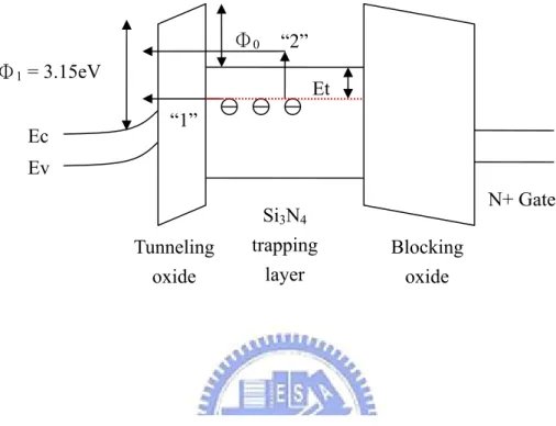
turn-on [2.2]. In SONOS memory device with SiO2 tunnel dielectric, the electrons and
holes must tunnel through 3.15eV and 4.5eV energy barriers, respectively, to be injected into the Si3N4 charge trap layer. The energy band diagram during retention is
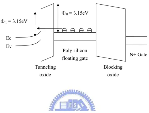
show in Fig. 2-1. It can compare to the FG structure band diagram during retention show in Fig. 2-2. For FG structure, the electrons injected from the channel are trapped in poly-silicon conduction band. For SONOS structure, the electrons injected from the channel are trapped in forbidden gap below the nitride conduction band (label with the trap energy level of Et). In this device, the electrons cannot move freely between the
discrete trap locations, hence the SONOS memory device is very robust against the defects inside the tunnel oxide and has better endurance than the floating gate flash memory. In the retention mode, electrons can leak to the substrae through the direct tunneling process shown as path “1” in Fig. 2-1. However, in this device the escape frequency is very small. Alternatively, electrons can be thermally de-trapped into the nitride conduction band and then tunnel back to the channel (this is path “2” in the fig. 2-1). This thermal de-trapping rate is exponentially reduced with a deep trap energy level. For these reasons, the SONOS flash memory can have much better retention time than the floating gate flash memory. A tunnel oxide of 3nm is thick enough to guarantee 10 years retention time in the SONOS flash memory.
That use silicon nanocrystals as the trapping material [2.4-2.5]. So the nanocrystal memory can robust against the defects inside the tunnel oxide like SONOS memory, and each dot will typically store only small amount of electrons. Collectively the charges stored in these dots control the channel-conductivity of the memory transistor.
As compared to conventional stacked-gate NVM devices, nanocrystal charge-storage offers several advantages, the main one being the potential to use thinner tunnel oxides without sacrificing nonvolatility. This is a quite attractive proposition, since reducing the tunnel oxide thickness is key to lowering operating voltages and/or increasing operating speeds. This claim of improved scalability results not only from the distributed nature of the charge storage, which makes the storage more robust and fault-tolerant, but also from the beneficial effects of Coulomb blockade [2.6]. Quantum confinement effects (band gap widening; energy quantization) can be exploited in sufficiently small nanocrystal geometries (sub-3 nm dot diameters) to further enhance the memory’s performance.
There are other important advantages though. First, nanocrystal memories use a more simplified fabrication process as compared to conventional stacked-gate FG NVM's by avoiding the fabrication complications and costs of a dual-poly process. Further, due to the absence of drain to FG coupling, nanocrystal memories suffer less from drain-induced-barrier-lowering (DIBL) and therefore have intrinsically better punchthrough characteristics. One way to exploit this advantage is to use a higher drain bias during the read operation, thus improving memory access time. Alternatively, it allows the use of shorter channel lengths and therefore smaller cell area (i.e., lower cost). Finally, nanocrystal memories are characterized by excellent immunity to stress induced leakage current (SILC) and oxide defects due to the distributed nature of the
charge storage in the nanocrystal layer.
For fabrication demand, a typical requirement the aerial density of nanocrystal dots is at least 1012cm-2. This is equivalent to approximately 100 particles controlling the channel of a memory FET with a 100 100 nm active area, and requires particle diameters of 5–6 nm and below. And the fabrication process should result in a planar nanocrystal layer, i.e., the thickness of the dielectric layer separating the nanocrystal and the substrate should be well controlled. Poor control of the tunnel oxide thickness will result in wider threshold voltage distributions and will increase the number of erratic bits. More generally, good process control is needed with regards to such nanocrystal features as: size and size distribution; inter-crystal interaction (lateral isolation); uniformity of aerial crystal density; and crystal doping (type and level). Finally, it is preferred that that the fabrication process is simple and that it uses standard semiconductor equipment.
Several nanocrystal fabrication processes have been demonstrated. King et al. [2.7] used Ge ion implantation subsequent high-temperature wet oxidation, which causes the implanted Ge atoms to pile up at the Si/SiO2 interface. And the number of
electrons trapped in the Ge nanocrystals was estimated to be 3.5×1012cm-2. Lin et al. [2.8] make HfO2 by co-sputtering with pure silicon (99.9999% pure) and pure
hafnium(99.9% pure) targets in an oxygen gas ambient deposition a 12-nm amorphous HfSiOx silicate layer. Then samples were subjected to RTA treatment in an O2 ambient
ambient to transfer the wetting layer into nanocrystals. This process is achieved through the relaxation of film stress and limited by the surface mobility [2.9]. Other than use deposition method, some special techniques formation nanocrystal are using ion implant [2.10-2.11] and sol-gel-spin-coating [2.12].
Nanocrystal memories have been presented in the midnineties as a possible alternative to conventional FG NVM devices, by allowing a further decrease in the tunnel oxide thickness. In particular, nanocrystal memories promise to enable a further scaling of the tunnel oxide, by relying on Coulomb blockade effects in small semiconductor geometries and on the enhanced robustness and fault-tolerance of distributed charge storage.
Research in this area has focused on the development of nanocrystal materials and fabrication processes, and on the integration of nanocrystal-based storage layers in actual memory devices. Promising device results have been presented, demonstrating low-voltage operation for comparable threshold voltage windows and operating speeds, and thin tunnel oxide retention behavior that suggest meeting long-term nonvolatility requirements.
In spite of these promising results, it is unclear whether nanocrystal memories will ever see commercialization. In order for that to happen, their claimed benefits will need to be more unambiguously substantiated, and a more appealing bundle of memory features will have to be demonstrated.
2.2 Memory basic concept
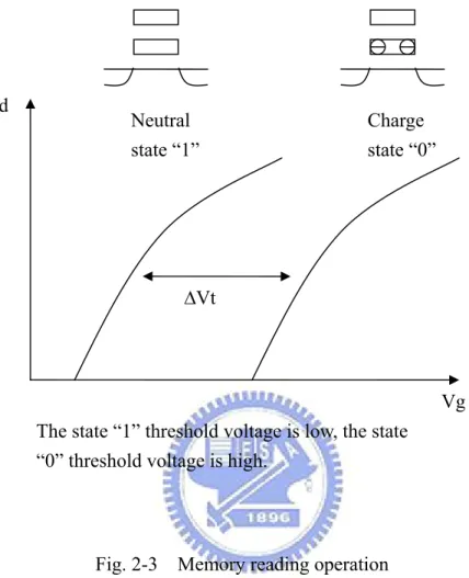
2.2.1 Reading operation
The data stored in a Flash cell can be determined measuring the threshold voltage of the memories. The best and fastest way to do that is by reading the current driven by the cell at a fixed gate bias show Fig. 2-3. When electrons stored in nanocrystal, the threshold voltage will shift (
∆
V
T ) that is proportional to the stored electron charge (Q). The threshold voltage shift of a Flash transistor can be written as [2.13-2.14]:T
Q
V
C
∆
= −
(2.1)
Here Q is the carge stored in nanocrystal, and C is the capacitance between nanocrystal and control gate. It is possible to fix a reading voltage in such way that the current of the “1” cell is very high (in the range of tens of microamperes), while the current of the “0” cell is zero, in the microampere scale. In this way, it is possible to define the logical state “1” from a microscopic point of view as no electron charge (or positive charge) stored in the nanocrystal and from a macroscopic point of view as large reading current. Vice versa, the logical state “0” is defined, respectively, by electron charge stored in the nanocrystal and zero reading current.
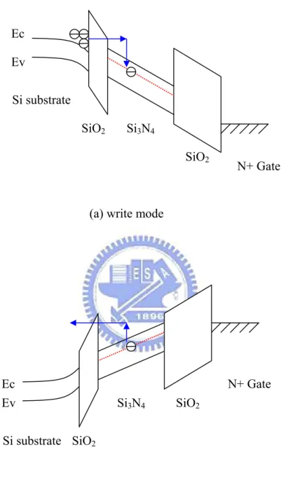
semiconductor memory device are illustrated schematically in Fig. 2-4. During the write process, a positive gate voltage is applied to inject channel inversion-layer electrons into the nitride layer. During the erase process, a reverse gate bias is applied to cause the electrons to tunnel back into the channel and the accumulation layer holes to tunnel into the nitride from the channel. There are many ways to achieve “programming” or “erasing”. In general, hot carrier electron injection and Fowler-Nordheim tunneling (F-N tunneling) are two kinds of common operation mechanism employed in novel nonvolatile memories.
2.2.2.1 Channel Hot-Electron Injection (CHEI)
The physical mechanism of CHEI is relatively simple to understand. An electron traveling from the source to the drain gains energy from the lateral electric field and loses energy to the lattice vibrations (acoustic and optical phonons). At low fields, this is a dynamic equilibrium condition, which holds until the field strength reaches approximately 100kV/cm [2.15]. For fields exceeding this value, electrons are no longer in equilibrium with the lattice, and their energy relative to the conduction band edge begins to increase. Electrons are “heated” by the high lateral electric field, and a small fraction of them have enough energy to surmount the barrier between oxide and silicon conduction band edges. Fig. 2-5 shows schematic representation of CHEI MOSFET and the energy-distribution function with different fields. In the other hand, the effective mass of hole is heavier than one of electron. It is too hard to obtain enough energy to surmount oxide barrier. Therefore, hot-hole injection rarely is employed in nonvolatile memory operation.
2.2.2.2 F-N tunneling
Tunneling is another way writes electrons into nanocrystal from substrate. But during retention electrons could tunnel back to the channel too, constituting a large leakage current. The magnitude of the leakage current depends on both the thickness and the electron barrier height of the tunnel dielectric. The tunneling probability is expressed as: 0
( )*
exp( 2
dx
m
e)
T
=
−
∫
φ
dx
=
(2.2)
Here
φ
( )
x
is barrier height. It is 3.1eV in Si-SiO2 for electrons see Table 2.1[2.16-2.20]. d is tunnel dielectric thickness,
=
the Planck’s constant and me is theelectron mass inside the tunnel dielectric and it is 0.5m0 for both nitride and oxide.
Many tunneling species can achieve charge transfer. Among them, in the memory operation mechanism, F-N tunneling is most often mentioned. The F-N tunneling mechanism occurs when applying a strong electric field (in the range of 8–10MV/cm) across a thin oxide. In these conditions, the energy band diagram of the oxide region is very steep. Therefore, there is a high probability of electrons passing through the energy barrier itself. The F-N tunneling [2.20] which can be expressed as follow:
total thickness of the tunnel and control oxide. As shown in Fig. 2-6, when the voltage drop across the tunnel dielectric exceeds the electron tunnel barrier height
φ
B, F-Ntunneling current depends more on the tunnel barrier height than on the tunnel dielectric thickness. Increasing the tunnel dielectric thickness will not decrease the tunneling current if the same electric field is applied.
2.2.2.3 Direct Tunneling
For nanocrystal memories, the control-gate coupling ratio of nanocrystal memory devices is inherently small. As a result, FN tunneling cannot serve as an efficient write/erase mechanism when a relatively thick tunnel oxide is used, because the strong electric field cannot be confined in one oxide layer. The direct tunneling is employed in nanocrystal memories instead. In the other hand, the direct tunneling is more sensitive to the barrier width than barrier height, two to four orders of magnitude reduction in leakage current can still be achieved if large work function metals, such as Au or Pt.
2.2.3 Data retention
Any nonvolatile memory technology, Flash memories are specified to retain data for over ten years. This means the loss of charge stored in the memory must be as minimal as possible. In updated Flash technology, due to the small cell size, the capacitance is very small and at an operative programmed threshold shift—about 2 V—corresponds a number of electrons in the order of 103 to 104. A loss of 20% in this number (around 2–20 electrons lost per month) can lead to a wrong read of the cell and then to a data loss. Possible causes of charge loss are: 1) defects in the tunnel oxide; 2)
defects in the interpoly dielectric; 3) mobile ion contamination; and 4) detrapping of charge from insulating layers surrounding the FG [2.21].
2.2.4 Endurance
Flash products are specified for 105 write/erase cycles. Cycling is known to cause a fairly uniform wear-out of the cell performance, mainly due to tunnel oxide degradation, which eventually limits the endurance characteristics. The oxide defect will increase stress induce leakage current (SILC), that let electrons store in memory will be lost. Threshold voltage gradually recovery the initial value that before writing, the memory window will be close. Data retention after cycling is the issue that definitely limits the tunnel oxide thickness scaling. For very thin oxide, below 8–9 nm, the number of leaky cells becomes so large that even error-correction techniques cannot fix the problem.
Tunneling layer
Electron barrier (eV)
Hole barrier (eV)
SiO
23.15 4.7
SiN 2.4 1.8
Al
2O
32.9 4.3
HfO
21.6 3.3
Ta
2O
50.3 3.0
Ec Ev Φ1 = 3.15eV Tunneling oxide Blocking oxide Φ0 Et Si3N4 trapping layer N+ Gate “1” “2”
Ec Ev Φ1 = 3.15eV Tunneling oxide Blocking oxide Poly silicon
floating gate N+ Gate
Fig. 2-2 FG band diagram during retention mode Φ0 = 3.15eV
Id Vg Neutral state “1” Charge state “0” ∆Vt
The state “1” threshold voltage is low, the state “0” threshold voltage is high.
Fig. 2-4 Memory band diagram in (a)write mode (b)Erase mode Ec Ev N+ Gate Si substrate SiO2 SiO2 Si3N4
(a) write mode
Ec Ev N+ Gate Si substrate SiO2 SiO2 Si3N4 (b) erase mode
Fig. 2-5 The procedure of channel hot electrons injection N+ N+ P substrate VD > 0V VG > 0V Si substrate Tox Φ1 Φ2
Chapter 3
Metal nanocrystal memory use Co
nanodot
3.1 Motivation
Memory with discrete charge elements allows more advanced scaling of tunneling oxide and exhibit superior characteristics compared to conventional FG structure memories in terms of operation voltage, write/erase speed, retention and endurance [3.1-3.4]. Scaling tunneling oxide can increase write/erase speed, but simultaneous decrease data retention because of increase electrons tunneling back to substrate from nanocrystals. For the data retention characteristics, however, have not provided sufficient nonvolatility mainly due to the high leakage current of ultrathin SiO2
tunneling barrier. Metal NC has been proposed in [3.5-3.8] aiming to improve the data retention. Since there are many kinds of metals that have the greater work function than silicon (Pt 5.29eV, Ni 4.84eV, Co 4.18eV), the electrons trapped in such metal NC are less likely to tunnel back to the substrate due to the higher electron barrier height, resulting in the prolonged data retention time. And due to the absence of drain to FG coupling, nanocrystal memories suffer less from drain induced barrier lowering (DIBL) and therefore have intrinsically better punchthrough characteristics. In addition, the large variety of the metal work functions from various metals allows more design flexibility in such device application. Besides for data retention goal, used discrete
storage still one advantage. The advantage is it can store two different data in only one device (i.e. one bit stored near drain side, other one store near source side, see Fig. 3-1) [3.9-3.10]. That can effective use each device and increase the memory size but don’t increase die size. The cost will be lower than one bit memory device.
3.2 Experimental procedure
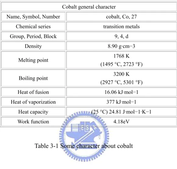
For manufacture nonvolatile memory device, we used P-type (100) silicon wafer. After RCA clean, growth tunneling oxide by furnace system. The oxide measured by ellipsometer is 35~38 Ǻ. Then used E-Gun evaporator deposited Co wetting layer about 40 Ǻ. This Co wetting lay thickness used 40 Ǻ refer to Liu’s paper [3.7-3.8] and Lee’s paper [3.11]. Some characters about cobalt list in Table 3-1. Then used rapid thermal process (RTP) anneal system of 400℃ ~ 900℃ in N2 and O2 ambient was
then performed to transform cobalt wetting-layer into cobalt nanocrystals. The split table show in the Table 3-2. The blocking oxide used PE-CVD method deposited about 250 Ǻ SiO2 for isolation each nanodots. Final deposited Al layer in front and back side
as electrode. Here, we use shadow mask in front side to define the cell pattern. The process flowchart show in Fig. 3-2.
The basic procedures for metal nanocrystal formation are starting with Si wafer covered by a thin layer of thermal oxide, a metal wetting layer of 1–5 nm is deposited by e-beam evaporation. Then, the film is annealed at elevated temperatures close to its eutectic temperature with the substrate in an inert ambient to transfer the wetting layer into nanocrystals. This process is achieved through the relaxation of film stress and limited by the surface mobility. Some long-range forces such as the dispersion force and the electrical double layers will also affect the nanocrystal size and location distributions [3.12-3.13].
Before RTA, the as-deposited film comes naturally with some thickness perturbation and even nanocrystals start to form (without a clear separation in between, though). When the film is RTA treated to give the atoms enough surface mobility, the film will self-assemble into a lower-total-energy state. To reduce the elastic energy carried by the stress built into the film during the deposition process, the film tends to break into islands along the initial perturbation. However, minimization of the surface energy and the dispersion force between the top and bottom interfaces can help stabilize the film. So the final geometry will depend on the balance between these driving forces. Once the nanocrystals have formed, the work function difference between the metal and the extrinsic substrate generates localized depletion or accumulation region in the substrate. The repulsion force between those regions helps stabilize the nanocrystals and keep a uniform distance between them.
Fig. 3-3 ~ Fig. 3-7 shows the AFM pictures of nanocrystal formation from Co films on top of 3.5 nm thermal oxide and the resulted nanocrystal size distribution. All samples went through the annealing cycle at different temperature for 30s and 60s. After RTA, well-defined nanocrystals with round shape and certain size distribution
can be achieved. The density of NC is decreased and the size of NC is increased as the RTA annealing temperature is increased. These results show that the greater thermal energy induced agglomeration of the metal wetting layer into the larger NCs. For sample6, we observe very dense nanocrystal formation. It be estimated about 3×1011cm-2. For the sample7、 sample8、 sample9 and sample10, the dot is baldly bigger than the sample6. But sample6 density is the highest. The higher treatment temperature and time, dots growth larger and the density decreased is agreeable we anticipation. The density for each sample are 1.6×1011cm-2 (sample7)、1.37×1011cm-2
(sample8)、0.971×1011cm-2 (sample9)、0.556×1011cm-2 (sample10).
3.3.2 Memory characteristics
In order to confirm the memory operation, high-frequency capacitance–voltage (HF C–V) characteristic of a capacitor with a SiO2 –cobalt NC–SiO2 –Al stack was
measured, as shown in Fig. 3-9 ~ Fig. 3-12. The observed large hysteresis in HF C–V indicates the charging and discharging process of the NC memory cell. The C-V curves are fail when samples treatment at low temperature (700℃). We guess maybe the metal film treat at low temperature not get enough energy translate film to nanodots. But sample7 although treatment at 700℃, but it C-V curve not express any memory character too. From sample AFM picture Fig. 3-3 and Fig. 3-4, although the dots have formation, but maybe not clear separation in each dot, so that these sample(sample6
design. In these samples, we found the sample8 have a larger flat-band voltage shift than other sample. It have more charge injection into cobalt NCs. And the sample9, it have a flat-band voltage shift up to 2 V too, but operating voltage is higher than sample8. The sample10 observe from its C-V curve, even then gate bias sweeps between 8V and -8V but not express memory window. And the sample10 AFM picture Fig.3-7, we look the lower dot density than other sample (sample10 only 5.56×1010cm-2). It maybe a reason explain this phenomenon. In RTO sample we observe each samples have stable C-V curve Fig. 3-8 but not show any memory window. Maybe the Co’s metal-oxide hasn’t trap ability.
3.3.3 Programming/Erase characteristics
Programming transient characteristics of cobalt NC memory devices are demonstrate in Fig. 3-13. Only programming in a low voltage 5V can get an obvious flat-band voltage shift. This is due to the fact that cobalt NC provides considerably greater density of available energy states, resulting in the larger amount of electrons stored inside the NC after programming. We compare Fig. 3-13 and Fig. 3-17, we find in the same programming voltage, sample8 flat-band voltage shift is larger than sample9. This is matching our measure in C-V curve. When operate in Erasing mode the gate apply negative bias, operation time over 0.01s the over-erase situation take place see Fig. 3-14. It maybe the hole be writing into NCs from channel or the free electrons in the cobalt be erasing.
Fig. 3-15 and Fig. 3-19 illustrated the retention characteristics of Co NCs at the room temperature. The retention time is very poor for a nonvolatile memory. The charge loss 76% and it can’t reach 10 year data retention. Sample9 only remain 0.264V flat-band voltage shift and sample10 remain 0.173V flat-band voltage shift. Some charge loss reasons have be mention in chapter 2. In these reasons, we guess the PE-oxide maybe a main reason for charge loses. Because dots in the surface, their inter-distance are very close only tens nanometer. If PE-oxide quality not very good, it will cause large charge loss in NCs. The blocking oxide leakage current illustrated in Fig. 3-21. Except for this reason, according to Liu’s paper [3.7] some dots have inter-connect will induce large leakage current show in Fig. 3-21. The tunneling oxide defect also can make large charge lose, but other experiment can prove the furnace system is clear. One reason can make the tunneling oxide defect generate. When metal film deposition on the tunneling oxide, it rely on heating process to translate metal film into dots. This process is achieved through the relaxation of metal film stress. During stress relaxation, maybe underlay oxide stand the stress. Make the oxide crack or defect generate so that the leakage current get more. Fig. 3-16 and Fig. 3-20 show these samples leakage current.
Cobalt general character
Name, Symbol, Number cobalt, Co, 27 Chemical series transition metals Group, Period, Block 9, 4, d
Density 8.90 g·cm−3
Melting point 1768 K
(1495 °C, 2723 °F)
Boiling point 3200 K
(2927 °C, 5301 °F) Heat of fusion 16.06 kJ·mol−1 Heat of vaporization 377 kJ·mol−1
Heat capacity (25 °C) 24.81 J·mol−1·K−1
Work function 4.18eV
Time (s)
Temperature
30s 60s
400℃
Sample1 Sample2
500℃
Sample3 Sample4
600℃
Sample5 Sample6
700℃
Sample7 Sample8
800℃
Sample9
900℃
Sample10
Source Drain
Substrate Control Gate(ploy)
Fig. 3-1 2-bit memory device
P type (100)
P type (100) P type substrate use pre-furnace RCA clean
Growth 35
Ǻ thin
oxide as tunneling
oxide
P type (100)E-Gun evaporator
deposited Co
P type (100)Use RTA system
transform Co layer
to nanodots
P type (100)Deposite 250 Ǻ
SiO
2Deposite Al as
electrode
Fig. 3-3 Co RTA 600℃ 60s sample AFM pictcure
Fig. 3-7 Co RTA 900℃ 30s sample AFM pictcure
-8 -6 -4 -2 0 1.0x10⁻¹¹ 2.0x10⁻¹¹ 3.0x10⁻¹¹ 4.0x10⁻¹¹ 5.0x10⁻¹¹ 6.0x10⁻¹¹ 7.0x10⁻¹¹ 8.0x10⁻¹¹ 9.0x10⁻¹¹ Capc itanc e VG 0 ~ -8v -8 ~ 0v RTO sample-8 -6 -4 -2 0 2 4 0.00E+000 5.00E-011 1.00E-010 1.50E-010 2.00E-010 2.50E-010 3.00E-010 capcitance VG 2v ~ -4v -4v ~ 2v 4v ~ -8v -8v ~ 4v
Fig. 3-9 RTA 700℃ 30s sample C-V curve
1.00E-010 1.50E-010 2.00E-010 2.50E-010 3.00E-010 3.50E-010 Capacitance 4v ~ -4v -4v ~ 4v 6v ~ -6v -6v ~ 6v 700oC 60s RTA
-6 -4 -2 0 2 4 6 0.00E+000 5.00E-011 1.00E-010 1.50E-010 2.00E-010 2.50E-010 3.00E-010 3.50E-010 Capaci tance VG 4v ~ -4v -4v ~ 4v 6v ~ -6v -6v ~ 6v 800oC 30s RTA
Fig. 3-11 RTA 800℃ 30s sample C-V curve
-10 -8 -6 -4 -2 0 2 4 6 8 10 2.00E-011 4.00E-011 6.00E-011 8.00E-011 1.00E-010 1.20E-010 1.40E-010 1.60E-010 1.80E-010 c apc it a n c e VG 8v ~ -8v -8v ~ 8v 900oC 30s RTA
1E-4 1E-3 0.01 0.1 1 0.0 0.1 0.2 0.3 0.4 0.5 0.6 0.7 0.8 0.9 1.0 1.1 1.2 1.3 1.4 V fb sh ift (V ) Time (s) 5v 7v 9v 11v 13v 15v
program at different voltage
Fig. 3-13 RTA 700℃ 60s sample program speed
0.0 0.2 0.4 0.6 0.8 1.0 V fb shift -6V -7V -8V not erase
10-1 100 101 102 103 104 105 106 107 108 20 30 40 50 60 70 80 90 100 110 No rm a liz e V fb s h ift ( % ) Time (s) 24% sample 8 data retention
Fig. 3-15 RTA 700℃ 60s sample data retention
-10 -8 -6 -4 -2 0 2 4 6 8 10 1E-12 1E-11 1E-10 1E-9 1E-8 0 ~ 10v 0 ~ -10v Lea k a g e current VG
700oC RTA leakage current
1E-4 1E-3 0.01 0.1 1 0.00 0.05 0.10 0.15 0.20 0.25 0.30 0.35 0.40 0.45 0.50 0.55 0.60 0.65 0.70 0.75 0.80 0.85 0.90 5v 7v 9v 11v 13v 15v V fb shi ft (V) Time (s)
800oC 30s sample program at different voltage
Fig. 3-17 RTA 800℃ 30s sample program speed
-0.1 0.0 0.1 0.2 0.3 0.4 0.5 0.6 V fb shi ft (V) -6v -7v -8v Erase at different gate voltage
10-1 100 101 102 103 104 105 106 107 108 20 30 40 50 60 70 80 90 100 110 No rmali z e V fb sh ift (% ) Time (s) 23% sample 9 data retention
Fig. 3-19 RTA 800℃ 30s sample data retention
-10 -8 -6 -4 -2 0 2 4 6 8 10 1E-10 1E-9 1E-8 1E-7 1E-6 1E-5 Le akage c u rrent VG 0 ~ 10v 0 ~ -10v 800oC RTA Leakage current
-10 -8 -6 -4 -2 0 2 4 6 8 10 1E-10 1E-9 1E-8 1E-7 1E-6 L eak ag e cu rr en t VG 0 ~ 10v 0 ~ -10v Oxide 25nm Leakage current
Chapter 4
Conclusions and recommendations
for future works
4.1 Conclusion
In this thesis “The memory characterization and investigation of metal nanocrystal”, we have investigated the memory effects and performance of cobalt metal nanocrystal memory devices. From our experiment, this memory can use low operation voltage to program and erase. But it has a big problem in data retention that is most important for nonvolatile memory. In our sample demonstrate poor data retention. It has some existing problem need analyze and solve that discuss in the before chapter. Maybe we can find another recipe (process) to improve this problem or maybe this metal is not suit for metal nanocrystal nonvolatile memory.
4.2 Recommendation for future works
1)
Use Co and SiO2 co-sputter that can let the Co dots surround by SiO2. It2) Find other metal material has large work function.
3) Used TEM analysis to find exactly dot density and some problems which make poor retention.
4) Use high-K material and metal dots simultaneously to improve data retention.
5) Use cobalt to manufacture nonvolatile memory device. Some high temperature process step in MOSFET manufacture after metal film anneal must be avoid. High temperature process can make metal dots unstable or affect other character. One high temperature process will be encounter that is after S/D implant anneal. We can use implant S/D and anneal before gate oxide growth. After S/D anneal, star gate oxide growth and following process. And use metal gate TiN can avoid in furnace system that to deposition poly-gate.
References
Chapter 1
[1.1] D. Kahng, S. M. Sze, “A Floating Gate and Its Application to Memory Devices,”
Bell Syst. Tech. Journal., vol. 46, pp. 1288-1295, 1967
[1.2] S. Lai, “Tunnel Oxide and ETOX Flash Scaling Limitation,” IEEE International
Non –Volatile Memory Conference, pp. 6 -7, 1998
[1.3] M. H. White, D. A. Adams, J. Bu, “On the Go with SONOS,” IEEE Circuits and
Devices Magazine., vol. 16, pp. 22-31, 2000
[1.4] H.E. Maes, J.S. Witters, G. Groeseneken, "Trends in non-volatile memory devices and technologies", Proceedings of the 17th
ESSDERC-conference, Invited paper, pp.
743-754, 1987, and in Solid State Devices, North Holland Publishing Company, Eds. G. Soncini, P.U. Calzolari, pp. 157-168, 1987
[1.5] S. Tiwari, F. Rana, K. Chan, H. Hanafi, C. Wei, and D. Buchanan, “Volatile and nonvolatile memories in silicon with nano-crystal storage,” in IEEE Int. Electron
Devices Meeting Tech. Dig., 1995, pp. 521–524.
[1.6] J. D. Blauwe, “Nanocrystal Nonvolatile Memory Devices,” IEEE Transactions on
Nanotechnology., vol. 1, pp. 72-77, 2002
[1.7] S. Tiwari, F. Rana, K. Chan, H. Hanafi, C. Wei, D. Buchanan, “Volatile and non-volatile memories in silicon with nano-crystal storage,” IEEE Int. Electron
[1.8] J. J. Welser, S. Tiwari, S. Rishton, K. Y. Lee, Y. Lee, “Room temperature
operation of a quantum-dot flash memory,” IEEE Electron Device Letters., vol. 18, pp. 278-280, 1997
[1.9] Y. C. King, T. J. King, C. Hu, “MOS memory using germanium nanocrystals formed by thermal oxidation of Si1-xGex,” IEEE Int. Electron Devices Meeting Tech. Dig., pp.115-118, 1998
Chapter 2
[2.1] M. White, Y. Yang, P. Ansha and M. L. French, “A low voltage SONOS nonvolatile semiconductor memory technology,” IEEE Transactions on Components,
Packaging and Manufacturing Technology, Vol.20, pp.190-195, 1997.
[2.2] M. K. Cho and D. M. Kim, “High performance SONOS memory cells free of drain turn-on and over-erase: compatibility issue with current flash technology”, IEEE
Electron Device Letters, pp.399-401, Vol.21, No.8, 2000.
[2.3] D. Kahng, S. M. Sze, “A Floating Gate and Its Application to Memory Devices,”
Bell Syst. Tech. Journal., vol. 46, pp. 1288-1295, 1967
[2.4] A. Fernandes, B. DeSalvo, T. Baron, J. F. Damlencourt, A. M. Papon,D. Lafond, D. Mariolle, B. Guillaumot, P. Besson, G. Ghibaudo, G. Pananakakis, F. Martin, and S.
Dig., 2002, pp. 181–184.
[2.6] J. J. Welser, S. Tiwari, S. Rishton, K. Y. Lee, and Y. Lee, “Room temperature operation of a quantum-dot flash memory,” IEEE Electron Device Lett., vol. 18, pp. 278–280, June 1997.
[2.7] Y. C. King , T. J. King and C. Hu, “Charge-trap memory device fabricated by oxidation of Si1-x Gex,” IEEE Trans. Electron Devices, vol 48, pp. 696-700, Apr. 2001.
[2.8] Y. H. Lin, C. H. Chien, C. T. Lin, C. Y. Chang, T. F. Lei, “Novel two-bit HfO/sub 2/ nanocrystal nonvolatile flash memory, ” IEEE Trans. Electron Devices, vol. 53,pp. 782-789, Apr. 2006
[2.9] Z. Liu, C. Lee, V. Narayanan, G. Pei, and E. C. Kan, “Metal nanocrystal memories—Part I: Device design and fabrication,” IEEE Trans. Electron Devices, vol. 49, pp. 1606-1613, Sept. 2002
[2.10] W. Eckstein, O. N. Gorshkov, A. P. Kasatkin, V. A. Novikov, D. I. Tetelbaum,S. A. Trushin, A. S. Ostashov, and A. N. Mikhailov, “Modeling of the formation and properties of nanocrystals in insulator matrices(SiO2:Si, ZrO2(Y):Zr) produced by ion
implantation,” in Conf. on Ion Implantation Technology, 2000, pp. 757–760.
[2.11] C. J. Nicklaw, M. P. Pagey, S. T. Pantelides, D. M. Fleetwood, R. D. Schrimpf, K. F. Galloway, J. E. Wittig, B. M. Howard, E. Taw, W. H. Mc- Neil, and J. F. Conley Jr., “Defects and nanocrystals generated by Si implantation ninto a-SiO2,” IEEE Trans.
[2.12] H. C. You, T. H. Hsu, F. H. Ko, J. W. Huang, T. F. Lei, “Hafnium Silicate Nanocrystal Memory Using Sol–Gel-Spin-Coating Method,” IEEE Electron Device
Lett., vol. 27, pp. 644–646, Aug. 2006
[2.13] P. Pavan, R. Bez, P. Olivo, E. Zanoni, “Flash memory cells—An overview,”
Proc. IEEE, vol. 85, pp. 1248-1271, 1997
[2.14] M. Woods, “Nonvolatile Semiconductor Memories: Technologies, Design, and Application,” C. Hu, Ed. New York: IEEE Press, (1991) ch. 3, pp. 59
[2.15] P. E. Cottrell, R. R. Troutman, T. H. Ning, “Hot-electron emission in n-channel IGFET's,” IEEE Journal of Solid-State Circuits, vol. 14, pp. 442-455, 1979
[2.16] J. Bu, M. H. White, “Design considerations in scaled. SONOS nonvolatile memory devices,”Solid State Electronics., vol. 45, pp. 113-120, 2001
[2.17] M. L. French, M. H. White, “Scaling of multidielectric nonvolatile SONOS memory structures,” Solid-State Electron., vol. 37, pp. 1913-1923, 1994
[2.18] M. L. French, C. Y. Chen, H. Sathianathan, M. H. White, “Design and scaling of a SONOS Multididectric device for nonvolatile memory applications,” IEEE Trans.
Comp. Pack. and Manu. Tech., part A, vol. 17, no. 3, pp. 390-397, 1994
Wiley, New York, 2002
[2.21] R. Bez, E. Camerlenghi, A. Modelli, A. Visconti, “Introduction to Flash Memory,” In Proc. of the IEEE, vol. 91, no. 4, pp. 489-502, 2003
Chapter 3
[3.1] S. Tiwari, F. Rana, K. Chab, H. Hanafi, C. Wei, and D. Buchanan, “Volatile and non-volatile memories in silicon with nano-crystal storage,” IEEE Int. Electron
Devices Meeting Tech. Dig., 521(1995)
[3.2] H.I. Hanafi, S. Tiwari, and I. Khan, “Fast and long retention-time nano-crystal memory,” IEEE Trans. Electron Devices, vol. 43, pp. 1553-1558, Sept. (1996).
[3.3] J. J. Welser, S. Tiwari, S. Rishton, K. Y. Lee, Y. Lee, “Room temperature
operation of a quantum-dot flash memory,” IEEE Electron Device Letters., vol. 18, pp. 278-280, 1997
[3.4] Y. C. King, T. J. King, C. Hu, “MOS memory using germanium nanocrystals formed by thermal oxidation of Si1-xGex,” IEEE Int. Electron Devices Meeting Tech. Dig., pp.115-118, 1998
[3.5] M. Takata, S. Kondoh, T. Sakaguchi, H. Choi, J. C. Shim, H. Kurino, and M. Koyanagi, “New nonvolatile memory with extremely high density metal nano-dots,” in IEDM Tech. Dig., 2003, pp. 553–556.
[3.6] C. Lee, A. Gorur-Seetharam, and E. C. Kan, “Operational and reliability comparison of discrete-storage nonvolatile memories: Advantages of single- and
double-layer metal NCs,” in IEDM Tech. Dig., 2003, pp. 557–560.
[3.7] Z. Liu, C. Lee, V. Narayanan, G. Pei, and E. C. Kan, “Metal NC memories-Part 1: Device design and fabrication,” IEEE Trans. Electron Devices, vol. 49, pp. 1606–1613, Sep. 2002.
[3.8] Z. Liu, C. Lee, V. Narayanan, G. Pei, and E. C. Kan, “Metal Nanocrystal Memories—Part II: Electrical Characteristics,” IEEE Trans. Electron Devices, vol. 49, pp. 1606-1613, Sept. 2002
[3.9] A. Datta, P. B. Kumar and S. Mahapatra, “Dual-Bit/Cell SONOS Flash EEPROMs: Impact of Channel Engineering on Programming Speed and Bit Coupling Effect,” IEEE Electron Device Letters., vol. 28, pp. 446 - 448, May. 2007
[3.10] Y. H. Lin, C. H. Chien, C. T. Lin, C. Y. Chang, “Novel Two-Bit HfO2
Nanocrystal Nonvolatile Flash Memory,” IEEE Trans. Electron Devices, vol. 53, pp. 782 - 789, Apr. 2006.
[3.11] J. J. Lee, Dim-Lee Kwong, “Metal nanocrystal memory with high-K tunneling barrier for improved data retention,” IEEE Trans. Electron Devices, vol. 52, pp. 507-511, Apr. 2005