536 IEEE ELECTRON DEVICE LETTERS, VOL. 32, NO. 4, APRIL 2011
Improved Power Conversion Efficiency of InGaN
Photovoltaic Devices Grown on Patterned
Sapphire Substrates
C. C. Yang, J. K. Sheu, C. H. Kuo, M. S. Huang, S. J. Tu, F. W. Huang,
M. L. Lee, Yu-Hsiang Yeh, X. W. Liang, and W. C. Lai
Abstract—The InGaN/sapphire-based photovoltaic (PV) cells with Al0.14Ga0.86N/In0.21Ga0.79N superlattice structures that
serve as absorption layers were grown on patterned sapphire substrates (PSSs). Under global air-mass 1.5 conditions, the short-circuit current density, the open-short-circuit voltage, and the fill factor obtained from the PV cells were 1.21 mA/cm2, 2.18 V, and 0.65, respectively, corresponding to a conversion efficiency of 1.71%. Compared with PV devices grown on flat sapphire substrates, the photocurrent of PSS-grown PV devices was enhanced by 26%. The improved PV performance was attributable to the positive effects of the PSS on the material quality.
Index Terms—InGaN, patterned sapphire substrate (PSS), photovoltaic (PV).
I. INTRODUCTION
S
INCE 2002, InGaN-based compounds for photovoltaic (PV) devices have been extensively discussed, mainly with regard to multiple quantum well [1], [2], p-i-n junction [3], [4], and short-period superlattice (SPS) designs [5], [6], due to their potential for applications in full-solar-spectrum absorption [7], [8]. The most common sapphire (Al2O3) substrates havebeen widely applied to light-emitting and laser diodes [9] and show a great potential for mass production and affordable prices for future PV applications. Although InGaN semiconductors for light-emitting devices show a little sensitivity to material qualities [e.g., threading dislocation (TD)] because of their unique quantum-dot-like localized states from indium-rich re-gions [10], the power conversion efficiency of InGaN-based PV devices is still low because of the sensitivity to structural defects in the InGaN absorption layer [2], [6]. To maintain the quality of InGaN alloys utilized in PV devices, the indium
Manuscript received January 5, 2011; accepted January 12, 2011. Date of publication February 24, 2011; date of current version March 23, 2011. This work was supported by the National Science Council under Grant NSC 97-2221-E-006-242-MY3. The review of this letter was arranged by Editor P. K.-L. Yu.
C. C. Yang, J. K. Sheu, M. S. Huang, S. J. Tu, F. W. Huang, X. W. Liang, and W. C. Lai are with the Institute of Electro-Optical Science and Engineering, Advanced Optoelectronic Technology Center, and the Center for Micro/Nano Science and Technology, National Cheng Kung University, Tainan 70101, Taiwan (e-mail: [email protected]).
C. H. Kuo is with the Institute of Lighting and Energy Photonics, National Chiao Tung University, Tainan 71150, Taiwan.
M. L. Lee and Y.-H. Yeh are with the Department of Electro-Optical Engineering, Southern Taiwan University, Tainan 71005, Taiwan (e-mail: [email protected]).
Color versions of one or more of the figures in this letter are available online at http://ieeexplore.ieee.org.
Digital Object Identifier 10.1109/LED.2011.2107725
contents need to be low (e.g., optical band gap around the ultraviolet regions), and the InGaN epilayer thickness needs to be within hundreds of nanometers to avoid generating excess TDs [9]. Several techniques, such as selective area growth and epitaxially lateral overgrowth for GaN/sapphire template sub-strates, have been developed to reduce the TD density to a lower level (∼6 × 107cm−2) [11], [12]. However, the epilayer might be as thick as tens of micrometers to achieve a low TD density, thereby smoothing the surface of GaN films. In contrast, back-mirror reflectors are utilized to increase the photocurrent up to 18.4% in the thin absorption layer [2], [4, and references within]. To further increase the photocurrent of InGaN-based PV devices, the indium contents must be raised to a higher level (e.g., visible-light regions) and reach an appropriate ab-sorption layer thickness. In this letter, the sapphire substrates with truncated-cone patterns were used to grow InGaN-based PV devices, and the related PV performance in electrical and optical properties were also shown in this letter.
II. EXPERIMENTS
InGaN epitaxial layers were deposited on c-face sapphire substrates by a commercial metal–organic vapor phase epitaxy reactor. Both a conventionally flat sapphire substrate (FSS) and a patterned sapphire substrate (PSS) were simultaneously used during the epitaxy process. The PSSs were prepared via con-ventional photolithography and dry-etching process. As shown in Fig. 1(a), the PSS featured truncated-cone patterns in the closely triangular package with a spacing of 1.5 μm. The height, top, and bottom diameters of each pattern were 1.5, 1.0, and 3.0 μm, respectively. The growth process involved a thin low-temperature GaN nucleation layer and a 4.0-μm-thick undoped-GaN (u-undoped-GaN) layer consisting of a 1.0-μm-thick u-undoped-GaN under a chamber pressure of 500 torr and a 3.0-μm-thick u-GaN grown under a pressure of 100 torr to feature lateral, coalescence, and quasi-2-D growth models to achieve a smooth surface.
Each step of u-GaN on the PSS is shown in Fig. 1(b) and (c), respectively. After both u-GaN template substrates were prepared, the main p-i-n structure, consisting of a 1-μm-thick Si-doped n+-GaN layer (n∼ 5 × 1018 cm−3), an undoped Al0.14Ga0.86N/In0.21Ga0.79N (4/3 nm for 14 pairs,
respec-tively) SPS layer, and a 0.1-μm-thick Mg-doped p-GaN (p∼ 5× 1017 cm−3) layer, was sequentially grown. The alloy contents and the layer thickness were calibrated by X-ray diffraction analyses based on a 100-nm-thick Al0.14Ga0.86N 0741-3106/$26.00 © 2011 IEEE
YANG et al.: IMPROVED POWER CONVERSION EFFICIENCY OF InGaN PV Devices 537
Fig. 1. Typical 45◦-tilt scanning-electron-microscope images of (a) the surface morphology of truncated-cone patterns on sapphire substrates, (b) u-GaN under 500 torr, and (c) the coalesced quasi-2-D growth of u-GaN deposited on the PSS.
Fig. 2. Relative EQE and room-temperature PL spectra measured by epitaxy structures grown on the FSS (PV-A) and the PSS (PV-B).
bulk layer and a 14-pair GaN/In0.21Ga0.79N SPS structure
de-posited on the u-GaN and/or FSS templates. Samples with epi-layer structures deposited on the FSS and the PSS were labeled as PV-A and PV-B, respectively. The device fabrication process was similar to our previous work [6], [13]. Finally, a 200-nm-thick SiO2antireflection layer was coated via plasma-enhanced
chemical-vapor deposition. The device area and the electrode coverage rate were 1× 1 mm2and 11.4%, respectively.
III. RESULTS ANDCONCLUSION
Fig. 2 shows the relative external quantum efficiency (EQE) room-temperature photoluminescence (PL) spectra as a func-tion of incident photon wavelengths and photon energy, respec-tively. A slight redshift in the absorption edge of PV-B was clearly observed, as compared with PV-A. This is consistent with the PL results, which characterized the peak positions of the PV-A and PV-B samples as 2.793 and 2.780 eV (444 and 446 nm), respectively. When the same p-i-n epilayer structure was simultaneously deposited on both substrates, the relatively thinner thickness of u-GaN on the PSS resulted in a relatively higher compressive strain (i.e., with an effectively larger c-axial length) [14]. Although this redshift could be beneficial for broader solar-spectrum absorption, it should be carefully con-sidered because the excess strain would eventually relax, gen-erating additional TDs to result in leakage paths in the PV devices.
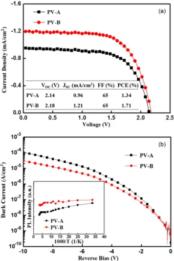
Fig. 3(a) shows the typical current-density–voltage (J –V ) characteristics and solar parameters measured under the global
Fig. 3. (a) Typical J –V characteristics of devices taken from the PV cells illuminated under the AM1.5G spectrum. (Inset) Measured PV parameters. (b) The measured dark current density with the reverse bias. (Inset) Arrhenius plots of integrated PL intensities for PV-A and PV-B.
air-mass 1.5 (AM1.5G) irradiance. Noteworthily, the PV-B samples with a relative lower optical band gap exhibited a higher open-circuit voltage VOC. VOC is strongly dependent
on the saturation current (or the reverse leakage current) of PV devices. At a given reverse bias of 10 V, the dark current density of the PV-B samples was measured to be 3.0× 10⁻⁵ A/cm2, which is lower than that of PV-A (1.1× 10⁻⁴A/cm2), as shown in Fig. 3(b). This improvement could be attributable to the slight reduction of the TD density by the lateral growth on the PSS [15]–[17]. Although a series of concaves on the PSS was filled with the u-GaN epitaxy associated with the bending of TDs, TDs in the epitaxial layers could be the primary factor behind the formation of trap states [18]. The leakage current in the
538 IEEE ELECTRON DEVICE LETTERS, VOL. 32, NO. 4, APRIL 2011
GaN/sapphire-based optoelectronic devices mainly originates from defect-related states that produce trap-assisted tunneling and/or recombination. In principle, the PV-B samples with a slightly lower optical band gap, as compared with the PV-A samples, would have a higher short-circuit current density (JSC). Compared with the PV-A samples, the calculated
en-hancement of JSCis within 10%. However, the measured JSC
of PV-B (1.21 mA/cm2) was enhanced by 26%, as compared with PV-A (0.96 mA/cm2). In addition to the small difference in the Egvalue of InGaN absorption layers between the PV-A and
PV-B samples, the increased JSCof PV-B is attributable to the
positive effects of the PSS. To clarify the influence of the PSS on the device efficiency, the relative internal quantum efficiency
ηint of the PV cells was indirectly evaluated via the intensity
integral of temperature-dependent PL spectra [19]. In principle, the thermal quench of luminescence in the absorption layer (Al0.14Ga0.86N/In0.21Ga0.79N superlattice) is mainly due to the
fact that carriers thermally escape from quantized states into the barrier states and/or are captured at nonradiative recombination centers in the active layers. The integrated PL (IPL) intensities as a function of temperature taken from PV-A and PV-B are displayed in the inset of Fig. 3(b). The IPL of both samples gradually declined with the increase in temperature. However, the decline rate of the IPL in PV-A was notably higher than that of PV-B, particularly when the temperatures were close to 300 K. This result indicates that the thermal quench of the IPL resulting from the capture at nonradiative recombination centers in PV-A had a relatively higher probability compared with that of PV-B. This result is consistent with the results that PV-B exhibited relatively higher JSC and VOC, as shown in
Fig. 3(a). The higher JSC value could be attributed to the fact
that photogenerated carriers recombined with defect-related centers in PV-B were relatively less than that in PV-A. On the other hand, the use of the PSS for the GaN/sapphire-based PV cells was beneficial to the reduction of TDs, which, in turn, leads to a reduction of the leakage current and, hence, the increase in VOCin PV-B.
In conclusion, the InGaN-based PV devices deposited on the PSS with truncated-cone patterns have been demonstrated. Enhancements by approximately 26% and 2% in terms of JSC
and VOC, respectively, as compared with the PV devices grown
on the FSS, have been obtained. The improved PV parameters could be attributable to the positive effects of the PSS on the material quality.
REFERENCES
[1] O. Jani, C. Honsberg, A. Asghar, D. Nicol, I. Ferguson, A. Doolittle, and S. Kurtz, “Characterization and analysis of InGaN photovoltaic devices,” in Proc. 31st IEEE PVSC, 2005, pp. 37–42.
[2] R. Dahal, J. Li, J. Y. Lin, and H. X. Jiang, “InGaN/GaN multiple quantum well concentrator solar cells,” Appl. Phys. Lett., vol. 97, no. 7, p. 073 115, Aug. 2010, and references therein.
[3] O. Jani, I. Ferguson, C. Honsberg, and S. Kurtz, “Design and charac-terization of GaN/InGaN solar cells,” Appl. Phys. Lett., vol. 91, no. 13, p. 132 117, Sep. 2007.
[4] R. H. Horng, M. T. Chu, H. R. Chen, W. Y. Liao, M. H. Wu, K. F. Chen, and D. S. Wuu, “Improved conversion efficiency of textured InGaN so-lar cells with interdigitated imbedded electrodes,” IEEE Electron Device
Lett., vol. 31, no. 6, pp. 585–587, Jun. 2010.
[5] J. K. Sheu, C. C. Yang, S. J. Tu, K. H. Chang, M. L. Lee, W. C. Lai, and L. C. Peng, “Demonstration of GaN-based solar cells with GaN/InGaN superlattice absorption layers,” IEEE Electron Device Lett., vol. 30, no. 3, pp. 225–227, Mar. 2009.
[6] C. C. Yang, J. K. Sheu, X. W. Liang, M. S. Huang, M. L. Lee, K. H. Chang, S. J. Tu, F. W. Huang, and W. C. Lai, “Enhancement of the conversion efficiency of GaN-based photovoltaic devices with AlGaN/InGaN absorption layers,” Appl. Phys. Lett., vol. 97, no. 2, p. 021 113, Jul. 2010.
[7] V. Y. Davydov, A. A. Klochikhin, R. P. Seisyan, V. V. Emtsev, S. V. Ivanov, F. Bechstedt, J. Furthmuller, H. Harima, A. V. Mudryi, J. Aderhold, O. Semchinova, and J. Graul, “Absorption and emission of hexagonal InN. Evidence of narrow fundamental band gap,” Phys. Stat. Sol. (B), vol. 229, no. 3, pp. R1–R3, Feb. 2002.
[8] J. Wu, W. Walukiewicz, K. M. Yu, J. W. Ager, III, E. E. Haller, H. Lu, W. J. Schaff, Y. Saito, and Y. Nanishi, “Unusual properties of the funda-mental band gap of InN,” Appl. Phys. Lett., vol. 80, no. 21, pp. 3967–3969, May 2002.
[9] S. Nakamura, “The roles of structural imperfections in InGaN-based blue light-emitting diodes and laser diodes,” Science, vol. 281, no. 5379, pp. 956–961, Aug. 1998.
[10] S. Chichibu, T. Azuhata, T. Sota, and S. Nakamura, “Spontaneous emis-sion of localized excitons in InGaN single and multiquantum well struc-tures,” Appl. Phys. Lett., vol. 69, no. 27, pp. 4188–4190, Dec. 1996, and references therein.
[11] A. Sakai, H. Sunakawa, and A. Usui, “Defect structure in selectively grown GaN films with low threading dislocation density,” Appl. Phys.
Lett., vol. 71, no. 16, pp. 2259–2261, Oct. 1997.
[12] S. Nakamura, M. Senoh, S. Nagahama, N. Iwasa, T. Yamada, T. Matsushita, H. Kiyoku, Y. Sugimoto, T. Kozaki, H. Umemoto, M. Sano, and K. Chocho, “Continuous-wave operation of InGaN/GaN/AlGaN-based laser diodes grown on GaN substrates,” Appl. Phys. Lett., vol. 72, no. 16, pp. 2014–2016, Apr. 1998.
[13] M. L. Lee, J. K. Sheu, and C. C. Hu, “Non-alloyed Cr/Au Ohmic contacts to n-GaN,” Appl. Phys. Lett., vol. 91, no. 18, p. 182 106, Oct. 2007. [14] K. Kusakabe, A. Kikuchi, and K. Kishino, “Characterization of overgrown
GaN layers on nano-columns grown by RF-molecular beam epitaxy,” Jpn.
J. Appl. Phys., vol. 40, pt. 2, no. 3A, pp. L192–L194, Mar. 2001, and
references therein.
[15] M. Yamada, T. Mitani, Y. Narukawa, S. Shioji, I. Niki, S. Sonobe, K. Deguchi, M. Sano, and T. Mukai, “InGaN-based near-ultraviolet and blue-light-emitting diodes with high external quantum efficiency using a patterned sapphire substrate and a mesh electrode,” Jpn. J. Appl. Phys., vol. 41, pt. 2, no. 12B, pp. L1 431–L1 433, Dec. 2002.
[16] S. Watanabe, N. Yamada, M. Nagashima, Y. Ueki, C. Sasaki, Y. Yamada, T. Taguchi, K. Tadatomo, H. Okagawa, and H. Kudo, “Internal quan-tum efficiency of high-efficient InxGa1−xN-based near-ultraviolet light-emitting diodes,” Appl. Phys. Lett., vol. 83, no. 24, pp. 4906–4908, Dec. 2003.
[17] W. K. Wang, D. S. Wuu, S. H. Lin, P. Han, R. H. Horng, T. C. Hsu, D. T. C. Huo, M. J. Jou, Y. H. Yu, and A. Lin, “Efficiency improvement of near-ultraviolet InGaN LEDs using patterned sapphire substrates,” IEEE
J. Quantum Electron., vol. 41, no. 11, pp. 1403–1409, Nov. 2005, and
references therein.
[18] J. K. Sheu, M. L. Lee, and W. C. Lai, “Effect of low-temperature-grown GaN cap layer on reduced leakage current of GaN Schottky diodes,” Appl.
Phys. Lett., vol. 86, no. 5, p. 052 103, Jan. 2005, and references therein.
[19] H. W. Huang, J. K. Huang, K. Y. Lee, C. F. Lin, and H. C. Kuo, “Light-output-power enhancement of GaN-based light-emitting diodes on an n-GaN layer using a SiO2 photonic quasi-crystal overgrowth,” IEEE