國立交通大學
電子工程學系 電子研究所
碩 士 論 文
新穎六層
k
‧
p
模擬器用於受應力(001)及(110)P型複晶矽,全矽化
及金屬閘極P通道金氧半場效電晶體之閘極電洞穿隧電流
A Novel Six-Band k‧p Simulator for Hole Gate
Tunneling Current in (001) and (110) Strained
pMOSFETs with Polysilicon, FUSI, and Metal Gates
研 究 生: 彭霖祥 Lim-Shyang Pee
指導教授: 陳明哲 博士 Prof. Ming-Jer Chen
新穎六層
k
‧p
模擬器用於受應力(001)及(110)P型複晶矽,全矽化及金 屬閘極P通道金氧半場效電晶體之閘極電洞穿隧電流A Novel Six-Band k‧p Simulator for Hole Gate Tunneling Current in
(001) and (110) Strained pMOSFETs with Polysilicon, FUSI, and
Metal Gates
研究生:彭霖祥 Lim-Shyang Pee
指導教授:陳明哲 Prof. Ming-Jer Chen
國立交通大學
電子工程學系 電子研究所
碩士論文
A Thesis
Submitted to Department of Electronics Engineering &
Institute of Electronics
College of Electrical and Computer Engineering
National Chiao Tung University
in Partial Fulfillment of the Requirements
for the Degree of
Master of Science
in
Electronics Engineering
August 2011
Hsinchu, Taiwan, Republic of China
I
新穎六層
k
‧
p
模擬器用於受應力(001)及(110)
P型複晶矽,全矽化及金屬閘極P通道金氧半場
效電晶體之閘極電洞穿隧電流
研究生: 彭霖祥 指導教授: 陳明哲 博士
國立交通大學
電子工程學系 電子研究所碩士班
摘要
本論文所提出嶄新進階式有效質量近似的演算法可以直接且有效的計算受 應力下(001)及(110)晶向P通道金氧半場效電晶體的閘極電洞穿隧電流.文中也 提及傳統的六層 kp 模型及舊式與進階式的有效質量近似的比較.此演算法已透 過幾道程序性的驗證,如(一)自身若合符節的電容與閘極電壓曲線重建;(二) 在受應力下的P型複晶矽,全矽化(FUSI)及金屬閘極P通道金氧半電晶體 晶都有令人滿意的實驗值與模擬值的比較;(三)應力值達負3GPa對遷移率 的增益與已發表的文獻相當一致;以及(四)在有應力及沒有應力的鰭式場效電 晶體(FinFET)(110)側壁所發表的文獻實驗值也一一被重建出來. 除此之外,透過此進階式有效質量近似的演算法,我們可以觀察與分析在P型複 晶矽閘極P通道金氧半電晶體(負1.83 GPA)與全矽化閘極P通道金氧半電 晶體(負2.29 GPA)所造成閘極電洞穿隧電流不同的起因.
II
A Novel Six-Band k‧p Simulator for Hole Gate
Tunneling Current in (001) and (110) Strained
pMOSFETs with Polysilicon, FUSI, and Metal Gates
Student: Lim-Shyang Pee Advisor: Dr. Ming-Jer Chen
Department of Electronics Engineering and Institute of Electronics
National Chiao Tung University
Abstract
We present an enhanced effective mass approximation (eEMA) algorithm with which one can straightforwardly calculate hole gate tunneling current Ig in (001) and (110) uniaxial compressive strained p-MOSFETs. The differences among the conventional EMA, enhanced EMA, and sophisticated six-band k dot p results are demonstrated. The algorithm is systematically validated in the various ways: (i) self-consistent Cg-Vg curve reproduction; (ii) satisfactory fitting of existing strain altered Ig data for both polysilicon, fully-silicided (FUSI), and metal gates; (iii) good agreement with literature mobility enhancement values for stress up to -3 GPa; and (iv) reasonable fitting of available experimental Ig-Vg curves in (110) sidewall-surface p-FinFETs with and without the stress. Moreover, with the use of the algorithm we can examine the origins of the observed Ig difference between polysilicon gate p-MOSFETs (-1.83 GPa) and FUSI ones (-2.29 GPa).
III
Acknowledgements
My wonderful time at 309A passed quickly, but it left me a lot of sweet
and unforgettable memories. It is my great honor to meet Prof. Chen,
and to have him to be my advisor. Thanks to Prof. Chen for the guidance
and tutor on my master study and even the morals of being human. I will
always remember the useful “slogan” that you always remind us on
research: back to the origin. Thanks to my dearest family for
encouraging me all the time either mentally or financially. Thanks to my
“boss”, C.C. Lee for providing instruction and assistance on my research,
it is my pleasure to work and cooperate with you.
IV
Contents
Chinese Abstract ... I English Abstract ... II Acknowledgements ... III Contents ... IV Figure Captions ... VI Table Captions ... XI Chapter 1 Introduction ... 1Chapter 2 Enhanced EMA Algorithm ... 3
2.1 Introduction ... 3
2.2 Strain and Surface Orientation ... 3
2.2.1 k‧p Hamiltonian... 3
2.2.2 Stress Effect ... 4
2.2.3 Surface Orientation Effect ... 5
2.3 Enhanced EMA (eEMA) Algorithm ... 6
2.4 Validation of eEMA ... 8
Chapter 3 eEMA Orientated Simulation Results ... 10
Introduction ... 10
3.1 Capacitance versus Gate Voltage ... 10
3.2 Hole Gate Direct Tunneling Current ... 11
3.2.1 Physical Model... 11
3.2.2Simulation Result and Discussion ... 13
Chapter 4 Individual Contributions to 40% Gate Current Reduction in FUSI Gate Strained (001) p-MOSFETs ... 15
V
4.2 Parameter Extraction ... 15
4.3 Simulation Result and Discussion ... 16
Chapter 5 Conclusion ... 18
VI
Figure Captions
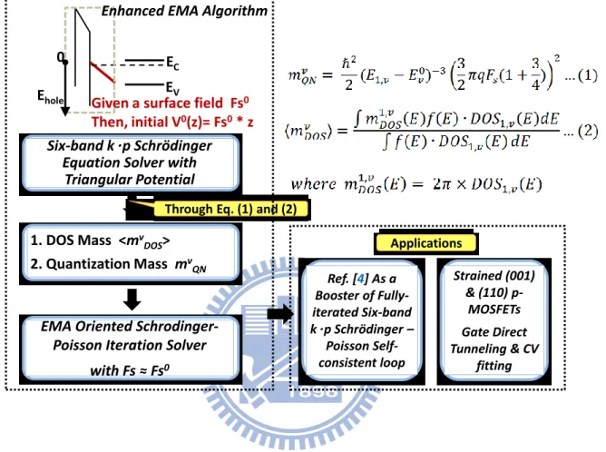
Fig. 2.1The flowchart of our enhanced EMA algorithm. In the inserted equations, 𝐸1, 𝑣 is the first subband of the 𝑣th bulk band 𝐸𝑣0, and 𝐷𝑂𝑆1, 𝑣𝐸 is the density-of-states function for 𝐸1, 𝑣. 𝐹𝑠 is the surface field, 𝑞 is the free electron charge, and 𝑓(𝐸) is the Fermi-Dirac distribution. ... 24 Fig. 2.2 The device structures for (001) and (110) p-MOSFETs. The channel
direction and applied stress direction are clarified. Here, only the favorable longitudinal compressive stress is under study. ... 25 Fig. 2.4.1 The resulting (001) effective masses for H1 bulk band versus
surface bending. The heavy, light, and split-off holes, for each subband energy, are mixed due to the coupling effect from the surface quantum confinement or the strain effect [7]. Therefore, we group the subband energies mainly according to the three lowest bulk bands, 𝐸10(H1), 𝐸20(H2), and 𝐸30(H3). ... 27 Fig. 2.4.2 The resulting (001) effective masses for H2 bulk band. The orange
dashed lines refer to the constant effective masses as in unstressed conditions. ... 28 Fig. 2.4.3 The resulting (001) effective masses for H3 bulk band. ... 29 Fig. 2.4.4 The resulting (110) effective masses for H1 bulk band. Only H1
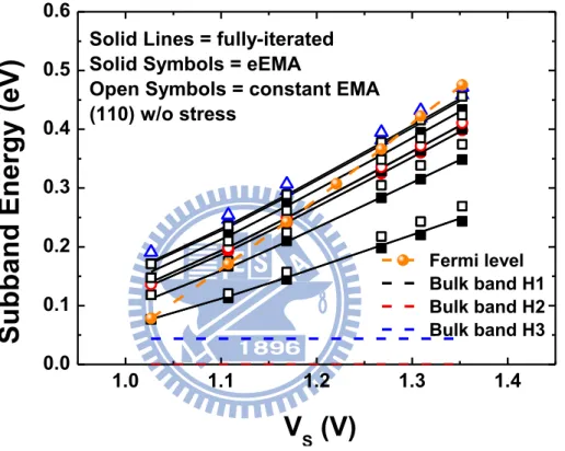
and H2 bulk bands are shown in (110) case here because of their high occupation in the subband energies. Note that (110) 𝑚𝑄𝑁𝐻1 is stress sensitive... 30 Fig. 2.4.5 The resulting (110) effective masses for H2 bulk band. ... 31 Fig. 2.4.6 The comparison of subband energy of (001) without stress among fully-iterated, eEMA and constant EMA. ... 32 Fig. 2.4.7 The comparison of subband energy of (001) under longitudinal
VII
EMA. ... 33 Fig 2.4.8 The comparison of subband energy of (001) under longitudinal
compressive stress 3 GPa among fully-iterated, eEMA and constant EMA. ... 34 Fig. 2.4.9 The comparison of subband energy of (110) without stress among
fully-iterated, eEMA and constant EMA. ... 35 Fig. 2.4.10 The comparison of subband energy of (110) under longitudinal
compressive stress 1 GPa among fully-iterated, eEMA and constant EMA. ... 36 Fig. 2.4.11 The comparison of subband energy of (110) under longitudinal
compressive stress 3 GPa among fully-iterated, eEMA and constant EMA. ... 37 Fig. 3.1.1 The comparison of calculated non-stress (001) gate capacitance
versus gate voltage from the constant EMA and enhanced EMA with the sophisticated six-band k·p results. ... 38 Fig. 3.1.2 The comparison of calculated non-stress (110) gate capacitance
versus gate voltage from the constant EMA and enhanced EMA with the sophisticated six-band k·p results. ... 39 Fig. 3.2.2.1 The calculated hole gate direct tunneling current density for (001)
and (110) p-MOSFETs under the longitudinal stress conditions of 0, -1, and -3 GPa. It is contributed by four parts: 1) F𝑖,𝑣 impact frequency of hole wave packet on interface, 2) n𝑖,𝑣(𝐸)inversion carrier density per energy, 3) 𝑇𝑖,𝑣𝑊𝐾𝐵 WKB part of transmission probability through
insulator, and 4) T𝑖,𝑣𝑅 reflection part of transmission probability through
insulator. ... 40 Fig. 3.2.2.2 The contribution of the averaged impact frequency of hole wave
packet on interface for (001) and (110) p-MOSFETs under the
VIII
Fig. 3.2.2.3 The contributions of the total inversion carrier density for (001) and (110) p-MOSFETs under the longitudinal stress conditions of 0, -1, and -3 GPa... 42 Fig. 3.2.2.4 The contributions of the average WKB transmission probability
through insulator for (001) and (110) p-MOSFETs under the
longitudinal stress conditions of 0, -1, and -3 GPa. ... 43 Fig. 3.2.2.5 The contribution of the average reflection part of transmission
probability through insulator for (001) and (110) p-MOSFETs under the longitudinal stress conditions of 0, -1, and -3 GPa. ... 44 Fig. 3.2.2.6 Schematic of energy band diagram of (110) p-MOSFET to show
the effective mass correction in p+-poly gate region. The two group velocities are associated with the effective masses labeled. ... 45 Fig. 3.2.2.7 The comparison of experimental and calculated hole gate direct
tunneling current change versus stress. The bias conditions and process parameters in the calculation are close to the experimental ones, where |VG|~1V for polygate and |VG|~1.6V for metal gate. ... 46
Fig. 3.2.2.8 The calculated hole gate direct tunneling current change as in Fig. 3.3.2.7 but with the stress range largely widened. The inset shows simulated mobility enhancement and its comparison with [19]. ... 47 Fig. 3.2.2.9 The comparison of calculated hole gate direct tunneling current
for p-FinFET with those measured from (110) sidewall surface
p-FinFET [2]. ... 48 Fig. 3.2.2.10 The calculated hole gate direct tunneling current density for
(001) p-MOSFETs with polysilicon, FUSI and metal gates under the longitudinal stress conditions of 0 and -2.5 GPa. ... 49 Fig. 3.2.2.11 The calculated hole gate direct tunneling current density for
(110) p-MOSFETs with polysilicon, FUSI and metal gates under the longitudinal stress conditions of 0 and -2.5 GPa. ... 50
IX
Fig. 3.2.2.12 The calculated hole gate direct tunneling current change versus stress for (001) and (110) p-MOSFETs with polysilicon, FUSI and metal gates. ... 51 Fig. 4.2.1 Capacitance-voltage fitting through proposed eEMA on (100)
p-MOSFETs with polysilicon and FUSI gates. The experimental data is measured under large devices. FUSI imposes an extra compressive stress ~460 MPa on the underlying p-MOSFET channel region. Table I shows the extracted parameters. ... 52 Fig. 4.2.2 Jg versus gate overdrive fitting under the small dimension samples.
Solid symbols indicate the experimental data and open symbols with line indicate the calculated one. The gate overdrive is used to eliminate Vth roll-off appearing in FUSI gate as shown in insert, so both the inversion conditions are same: Vth(Lmask=1um) for the ideal calculation results and Vth(Lmask=0.036um) for the experimental results. ... 53 Fig. 4.3.1 Comparison of CV fitting on (100) p-MOSFETs with polysilicon
and FUSI gates. (a) without consideration of stress on FUSI gate. (b) Longitudinal compressive stress 460 MPa considered on FUSI gate, which fitted perfectly. ... 54 Fig. 4.3.2 Impact of polysilicon dopant concentration on (a)
capacitance-voltage curve and (b) Ig versus Vg . 𝑁𝑠𝑢𝑏 = 1 × 10¹⁸𝑐𝑚 − 3, 𝑇𝑜𝑥 = 1.3𝑛𝑚 , 𝑚𝑜𝑥 = 0.37𝑚0 , Stress =
Long. −1.83 GPa. ... 55 Fig. 4.3.3 Impact of Longitudinal compressive stress on (a)
capacitance-voltage curve and (b) Ig versus Vg . 𝑁𝑠𝑢𝑏 = 1 × 10¹⁸𝑐𝑚 − 3, 𝑇𝑜𝑥 = 1.3𝑛𝑚 , 𝑚𝑜𝑥 = 0.37𝑚0 , 𝑁𝑝𝑜𝑙𝑦 = 7 ×
1019𝑐𝑚 − 3. ... 56 Fig. 4.3.4 Impact of work function shift on (a) Capacitance-voltage curve and (b) Ig versus Vg . 𝑁𝑠𝑢𝑏 = 1 × 10¹⁸𝑐𝑚 − 3, 𝑇𝑜𝑥 = 1.3𝑛𝑚 , 𝑚𝑜𝑥 = 0.37𝑚0 , without stress. ... 57
X
Fig. 4.3.5 The calculated hole gate direct tunneling currents for polysilicon- and FUSI-gate p-MOSFETs and the comparison with two data points [24]. The inset depicts the five main contributions for the observed hole gate direct tunneling current difference. ... 58 Fig. 4.3.6 The comparison of work function of Ni FUSI gates among this
work, [26] and [27]. The additional dopants to polysilicon before silicidation result the shifts in work function. ... 59
XI
Table Captions
Table I. The extracted parameters for Fig 4.2.1 and 4.2.2.
Table II. Hole band, hole scattering and physical parameters used in this
work
1
Chapter 1
Introduction
Owing to the successful effective mass approximation (EMA) in inversion layers of n-MOSFETs, it is possible to develop a gate direct tunneling model [1]. However, in the presence of the anisotropic and non-parabolic properties around Γ point of the valence-band structure, the ability to quantitatively deal with the hole effective masses in p-MOSFETs has long been one of the challenging issues. Currently, both the strain engineering and the p-FinFET structure with (110) sidewall surface have raised this concern further [2]. Sophisticated simulations [3],[4] have already quantified hole effective masses, primarily on (001) surface only. Although there exist some works [5],[6] dedicated to the strain and (110) orientation effects on effective masses, extensions to the hole gate direct tunneling current Ig were not yet done. Even in the citation [2], a conversion from measured stress altered threshold voltage to effective mass change was needed prior to Ig calculation. Here, we propose an enhanced EMA algorithm, based on our recent work [4], to achieve the goal directly, without accounting for the conversion procedure [2].
Firstly, the flowchart of enhanced EMA will be explained in Chapter 2. The process of extracting the quantization and two-dimensional DOS effective masses will be demonstrated. In addition, the simulated effective masses will be shown with the accompanying subband energies. Next, the capacitance and gate direct tunneling current calculation under the varying stress and wafer orientations will be exhibited in Chapter 3. The supporting experimental results will be also shown and discussed. Then, Chapter 4 is devoted to examine the twofold difference in hole gate direct tunneling current between FUSI and polysilicon gate. Finally, the conclusions will be given in
2
3
Chapter 2
Enhanced EMA Algorithm
2.1 Introduction
It has been well recognized that in the context of the effective mass approximation (EMA), a two-dimensional electron gas (2DEG) system in n-channel MOSFETs can be visualized and described successfully in a quasi-classical manner. However, the valence-band structure of inversion layers in p-MOSFETs is much complicated in terms of strong anisotropy and nonparabolicity of the hole subbands. As discussed in our previous work [4], the effective masses enable the acceleration of fully iterated six-band k dot p Schrödinger and Poisson numerical loop. Here, we propose an enhanced EMA algorithm in order to calculate hole gate direct tunneling current Ig in (001) and (110) under strain effects. Fig. 2.1 shows the flowchart of our enhanced EMA algorithm. Fig. 2.2 clarifies the effects of the in-plane stress and channel direction in (001) and (110) p-MOSFETs. We will first discuss how the strain and surface orientation effect can be treated in our k‧p Hamiltonian Hkp. Then, we extract both the
quantization effective mass mQN and DOS effective mass mDOS, followed by the
validation of this proposed eEMA.
2.2 Strain and Surface Orientation
2.2.1 k‧p Hamiltonian
The k‧p Hamiltonian Hkp used in our algorithm is composed of two parts: the
Luttinger-Kohn Hamiltonian HLK and the strain Hamiltonian Hstrain. These expressions
4 1 0 2 2 3 0 2 2 3 0 2 2 1 0 2 2 1 3 2 2 0 2 2 3 1 2 2 0 2 2 kp LK strain P Q L M L M L P Q M Q L M P Q L L Q H H H M L P Q M L L Q L M P M L Q L P , (2.2.1.1) where k k k k P P P Q Q Q L L L M M M , (2.2.1.2)
2 2 2 2 1 0 2 2 2 2 2 0 2 3 0 2 2 2 2 3 0 2 2 2 3 3 2 2 k x y z k x y z k x y z k x y x y P k k k m Q k k k m L k ik k m M k k i k k m ;
2 2 3 2 v xx yy zz xx yy zz xz yz xx yy xy P a b Q L d i M b id . (2.2.1.3)The P , k Q , k L and k M are the k pk terms and the P, Q, L and M are the strain terms, which will be discussed later. The is the split-off energy. The Luttinger parameters 1, 2, 3 and strain deformation potentials a , v b, d are both listed in Table II.
2.2.2 Stress Effect
Strain describes the change of size and/or shape in response to external forces which are applied on a deformable body; however, stress is defined as the average amount of
5
force exerted per unit area. Gratefully, a general form originating from Hooke’s law was developed, which can adequately deal with the mechanics of materials, as expressed below [8] 𝜀𝑥𝑥 = 1 𝐸[𝜎𝑥𝑥− 𝜈(𝜎𝑦𝑦+ 𝜎𝑧𝑧)] (2.2.2.1𝑎) 𝜀𝑦𝑦 = 1 𝐸[𝜎𝑦𝑦− 𝜈(𝜎𝑥𝑥+ 𝜎𝑧𝑧)] (2.2.2.1𝑏) 𝜀𝑧𝑧 = 1 𝐸[𝜎𝑧𝑧− 𝜈(𝜎𝑥𝑥+ 𝜎𝑦𝑦)] (2.2.2.1𝑐) 𝛾𝑥𝑦= 1𝐺𝜏𝑥𝑦 , 𝛾𝑥𝑧 = 𝐺1𝜏𝑥𝑧 , 𝛾𝑦𝑧 =𝐺1𝜏𝑦𝑧 (2.2.2.1d) where σ𝑖𝑖 refers to the normal stress component acting on the planes perpendicular to i-direction, τ𝑖𝑗 indicates the shear stress components oriented in the j-direction acting
on the planes perpendicular to i-direction, 𝛾𝑖𝑗 denotes engineered shear strain, and 𝜀𝑖𝑗 is average shear strain defined as one half the 𝛾𝑖𝑗 [9], [10]. 𝐸, 𝜈 and 𝐺 represent the
Young’s modules, Poisson’s ratio and shear modulus of elasticity, respectively. We therefore establish the elastic strain-stress matrix in the following [11]:
[ 𝜀𝑥𝑥 𝜀𝑦𝑦 𝜀𝑧𝑧 2𝜀𝑦𝑧 2𝜀𝑧𝑥 2𝜀𝑥𝑦] = [ 𝑆11 𝑆12 𝑆12 0 0 0 𝑆12 𝑆11 𝑆12 0 0 0 𝑆12 𝑆12 𝑆11 0 0 0 0 0 0 𝑆44 0 0 0 0 0 0 𝑆44 0 0 0 0 0 0 𝑆44][ 𝜎𝑥𝑥 𝜎𝑦𝑦 𝜎𝑧𝑧 𝜏𝑦𝑧 𝜏𝑧𝑥 𝜏𝑥𝑦] (2.2.2.2)
where 𝑆11, 𝑆12 and 𝑆44 are the elastic stiffness constants. Those parameters used in our simulation are listed in Table II.
2.2.3 Surface Orientation Effect
Since the k‧p Hamiltonian Hkp is established under the (001) systems, we need to
do some appropriate rotations on k space for the purpose of dealing with (110), (111), (112) or even (11x) surface. For (110) surface, a rotation from the original (001) k space to (110) 𝑘′ is required:
6 𝑘𝑥′ = −𝑘𝑧 𝑘𝑦′ = 1 √2(𝑘𝑥− 𝑘𝑦) (2.2.3.1) 𝑘𝑧′ = 1 √2(𝑘𝑥+ 𝑘𝑦) for (111) surface: 𝑘𝑥′ = 1 √6(𝑘𝑥+ 𝑘𝑦− 𝑘𝑧) 𝑘𝑦′ = 1 √2(−𝑘𝑥+ 𝑘𝑦) (2.2.3.2) 𝑘𝑧′ = 1 √3(𝑘𝑥+ 𝑘𝑦+ 𝑘𝑧) and likely for (112) surface:
𝑘𝑥′ = 1 √3(𝑘𝑥+ 𝑘𝑦− 𝑘𝑧) 𝑘𝑦′ = 1 √2(−𝑘𝑥+ 𝑘𝑦) (2.2.3.3) 𝑘𝑧′ = 1 √6(𝑘𝑥+ 𝑘𝑦+ 2𝑘𝑧)
2.3 Enhanced EMA (eEMA) Algorithm
The self-consistent six-band k dot p simulation in inversion layers of p-MOSFETs is time-consuming. To simplify the hole subband structure calculation, a triangular-potential approximation may be employed [12]. In this algorithm, we first input an initial surface field to six-band k dot p schrodinger equation solver with triangular potential approximation. Each of the k states is systematically calculated on the decided kx-ky space accordingly. The outcomes of the triangular-potential-based
six-band k dot p simulator contain the constant-energy contours in the k plane, the subband energy levels, the surface potential, and the Fermi level Ef of the sysyem. The
7
E(𝑘) resulting from our six-band k‧p calculation can be used to derive the density-of –states function for holes in the valence-band for semiconductor of interest. The corresponding two-dimensional density-of-states (DOS) functions are determined in the Cartesian coordinate system by
𝐷𝑂𝑆1,𝑣(𝐸) = 𝑈(𝐸 − 𝐸1,𝑣)(2𝜋)1 2×𝐴𝑟𝑒𝑎1,𝑣𝑘−𝑠𝑝𝑎𝑐𝑒(𝐸:𝑑𝐸);𝐴𝑟𝑒𝑎1,𝑣𝑘−𝑠𝑝𝑎𝑐𝑒(𝐸)
𝑑𝐸 (2.3.1)
where the index v means the subband order up to the sixth lowest subband and U (E) means the unit step function of energy. The total DOS function is given as
𝐷𝑂𝑆𝑡𝑜𝑡𝑎𝑙(𝐸) = ∑ 𝐷𝑂𝑆1,𝑣(𝐸) 𝑣
(2.3.2) According to the calculations above, DOS effective mass of each subband is energy dependent, and each of them can be inversely extracted from simulated 𝐷𝑂𝑆1,𝑣(𝐸):
𝑚𝐷𝑂𝑆1,𝑣 (𝐸) = 2𝜋ℏ2× 𝐷𝑂𝑆
1,𝑣(𝐸) (2.3.3)
To obtain the DOS effective mass efficiently and accurately, we average them by 〈𝑚𝐷𝑂𝑆𝑣 〉 =∫ 𝑚𝐷𝑂𝑆
1,𝑣 (𝐸)𝑓(𝐸) ∙ 𝐷𝑂𝑆
1,𝑣(𝐸)𝑑𝐸
∫ 𝑓(𝐸) ∙ 𝐷𝑂𝑆1,𝑣(𝐸)𝑑𝐸
(2.3.4) Additionally, based on triangular potential approximation [13], the quantization effective mass, 𝑚𝑄𝑁𝑣 , can also be analytically derived as
𝑚𝑄𝑁𝑣 =ℏ2 2 (𝐸1,𝑣− 𝐸𝑣0) ;3 (3 2𝜋𝑞𝐹𝑠(1 + 3 4)) 2 (2.3.5) where 𝐸1,𝑣 is the first subband of the 𝑣th bulk band 𝐸𝑣0, and 𝐷𝑂𝑆
1,𝑣(𝐸) is the
density-of-states function for 𝐸1,𝑣. 𝐹𝑠 is the surface field, 𝑞 is the free electron charge,
and 𝑓(𝐸) is the Fermi-Dirac distribution. All the items above are from the results of the six-band k·p Schrödinger equation with the triangular potential approach. Worthy to note that the hole type distinguishing (e.g. heavy hole, light hole, and split-off hole, for each subband energy) is obscure due to the coupling between each other under the surface quantum confinement and/or the strain effect. The correlative study can be found in [14], which states that one subband may mix with three hole types. Therefore,
8
we group the subband energies mainly according to the three lowest bulk bands, 𝐸10,
𝐸20, and 𝐸
30 (we can say that 𝑣 = 1 for heavy hole, 𝑣 = 2 for light hole, and 𝑣 = 3
for split-off hole with no applied stress). To recognize them easily, we call the 𝑣 = 1 bulk band as H1, the 𝑣 = 2 bulk band as H2, and the 𝑣 = 3 bulk band as H3. For (001) case within the 0 to -3 GPa channel stress, we assume that the three lowest subband energies from triangular potential approach are 𝐸1,𝐻1, 𝐸1,𝐻2, and 𝐸1,𝐻3. But for (110)
case, the three lowest subband energies from triangular potential approach are 𝐸1,𝐻1, 𝐸2,𝐻1, and 𝐸1,𝐻2.
Until now, both effective masses are readily to be served in the last but the most important section. Analogous to the electron counterparts [15], [16], the simple EMA-oriented Schrödinger-Poisson iterative solving can be employed using the aforementioned effective masses in the condition of the output surface field must nearly equal to the initial surface field. The EMA-oriented Schrödinger-Poisson iterative solving in pMOSFETs is therefore as fast as the nMOSFET, and finally the outputs are readily to be used, since its validity is seriously examined that will be given in next section
2.4 Validation of eEMA
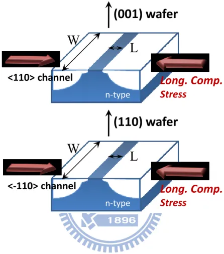
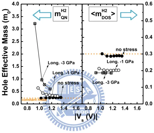
Fig. 2.4.1 to 2.4.5 show the effective masses of each bulk band on (001) and (110) surfaces as the valleys in electron counterpart. The H1 and H2 quantization masses on (001) can be approximated or treated reasonably well by constant mass just like what had been published elsewhere [17], [18]. However, the quantization mass of (110) should not be described by constant mass, since we can see that (110) H1 quantization effective mass increases rapidly because of the compressive channel stress. This is directly related to the stressed bulk heavy-hole constant energy surface as shown in
9
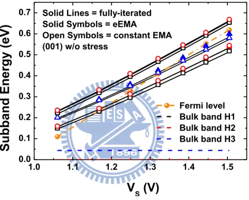
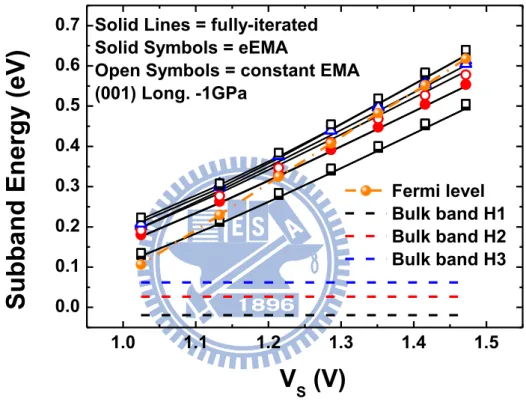
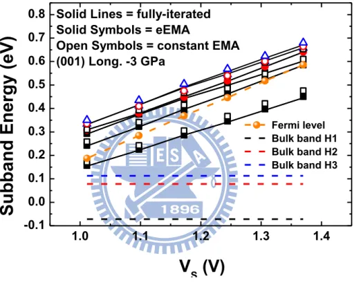
the insert of Fig. 2.4.4. Only H1 and H2 bands are shown in (110) case because they are the most dominant bands. To use both effective mass conveniently, surface band bending is labeled on x-scale, so they can directly be applied in Schrödinger and Poisson self-consistent calculation. Extremely huge CPU time is inevitable if one has to run the six-band k‧p calculation instead of using our simulation results. The corresponding subband energies and the subband comparison between the constant EMA, our enhanced EMA, and sophisticated six-band k·p results are also illustrated in Fig. 2.4.6 and 2.6.11. Thus, the validity of the enhanced EMA is confirmed by this comparison and it leads us to reach a clear conclusion: (i) the enhanced EMA remains its validity under various channel stresses on both (001) and (110) wafer orientations; and (ii) the result of enhanced EMA can find further application in gate capacitance and gate direct tunneling current.
10
Chapter 3
eEMA Orientated Simulation Results
Introduction
In this section, we check the reliability of our simulated capacitance and the hole gate direct tunneling current in (001) and (110) uniaxial compressive strained p-MOSFETs with the effective mass obtained from our enhanced effective mass approximation (eEMA). Then, we discuss the contributions of individual components and the effect of gate material on it.
3.1 Capacitance versus Gate Voltage
Owing to the voltage dependence of capacitance on both MOS and MOSFET, a more general expression for calculating capacitance is given as
𝐶 = |𝑑𝑄𝑠
𝑑𝑉𝐺| (3.1.1) where 𝑄𝑠 denotes the total charge on the semiconductor region. The calculated capacitance versus gate voltage curves are shown in Fig. 3.1.1 and 3.1.2 for unstressed (001) and (110) p-MOSFET. We adopt the effective masses listed in those figures in order to observe the distinctive differences among constant EMA, enhanced EMA, and fully-iterated results. Remarkably, a considerable discrepancy from the constant EMA is revealed in Fig. 3.1.2, due to much heavy (110) H1 quantization effective mass as shown in Fig. 2.4.4. Therefore, it is found that the effective masses must be treated properly as a consequence of extracting the process parameter. Only with this procedure can the subsequently calculated hole gate direct tunneling current be reasonable. The poly-gate doping, longitudinal compressive stress, and work function
11
dependence of (001) capacitance are shown theoretically in Fig. 4.3.2 (a), 4.3.3 (a), and 4.3.4 (a) with the enhanced EMA. Low poly-gate doping induces extra poly-gate capacitance in series that will finally cause the overall capacitance decrease, which is clearly demonstrated in Fig. 4.3.2 (a). Fig. 4.3.3 (a) shows the impact of poly-gate doping in weak inversion region, where the threshold voltage shift as the substrate doping and compressive stress increase. Moreover, different gate materials that result in diverse work functions can cause the capacitance shift according to our simulation, which is shown in Fig. 4.3.4 (a).
3.2 Hole Gate Direct Tunneling Current
3.2.1 Physical Model
By referring to [18], the hole current density contributed by the jth subband with energy E ranging from Ei,v, the subband of vth bulk band, to infinity can be written as
𝐽𝑖,𝑣 = ∫ 𝑞𝐸∞ 𝑖,𝑣 ∙ 𝐹𝑖,𝑣∙ 𝑛𝑖,𝑣(𝐸) ∙ 𝑇𝑖,𝑣 𝑊𝐾𝐵(𝐸) ∙ 𝑇 𝑖,𝑣𝑅(𝐸)𝑑𝐸 (3.2.1.1) 𝐽𝑔 = ∑ 𝐽𝑖,𝑣 𝑖,𝑣 (3.2.1.2) where q denotes the elemental charge, 𝐹𝑖,𝑣 is impact frequency of hole wave packet on interface, 𝑛𝑖,𝑣(𝐸) is inversion carrier density per energy, 𝑇𝑖,𝑣𝑊𝐾𝐵(𝐸) is transmission
probability through insulator of WKB part, 𝑇𝑖,𝑣𝑅(𝐸) is transmission probability
through reflection part of insulator and 𝑖 refers to the subband index while 𝑣 refers to bulk band index. There are 18 subbands considered in our calculation. These subbands are quantitatively and accurately enough in our simulation. The impact frequency can be described as
𝐹𝑖,𝑣 =qE𝑠 2 (2𝑚𝑄𝑁 𝑖 𝐸 𝑖,𝑣) ;12 (3.2.1.3) For the inversion carrier density, we calculate it through
12
𝑛𝑖,𝑣 = 𝑔𝑖𝑚𝐷𝑂𝑆𝑖
𝜋ℏ2 𝑘𝐵𝑇ln (1 + 𝑒 𝐸𝑓−𝐸𝑖,𝑣
𝑘𝑇 ) (3.2.1.4) where the degeneracy of ith subband 𝑔𝑖 is equal to 2. Among two terms in the
transmission probability through oxidelayer, the first one is WKB part, which can be modeled as 𝑇𝑖,𝑣𝑊𝐾𝐵(𝐸) = exp *−2 ℏ|∫ √2𝑚𝑜𝑥(𝐸 − 𝑞𝑉(𝑧))𝑑𝑧 𝑇𝑜𝑥 0 |+ = exp (4√2𝑚𝑜𝑥(𝜑𝑐𝑎𝑡 3/2 − 𝜑 𝑎𝑛3/2) 3𝑞ℏ|𝐸𝑜𝑥| ) (3.2.1.5) 𝜑𝑐𝑎𝑡 = 𝑞𝜒− 𝑞|𝐸𝑜𝑥|𝑇𝑜𝑥− 𝐸 (3.2.1.6) 𝜑𝑎𝑛 = 𝑞𝜒− 𝐸 (3.2.1.7)
where 𝜑𝑐𝑎𝑡 is the barrier height of the tunneling hole with total energy E at cathode side or gate/oxideinterface, and 𝜑𝑎𝑛 is that at anode side or oxide/n-well interface with
𝜒 is the barrier height of oxide/Si interface. Another one is 𝑇𝑖,𝑣𝑅(𝐸), which is given as
𝑇𝑖,𝑣𝑅(𝐸) = T 1𝑅 × T2𝑅 = 4𝑣𝑠𝑖,⊥(𝐸)𝑣𝑜𝑥(𝜑𝑎𝑛) 𝑣𝑠𝑖,⊥2 (𝐸) + 𝑣 𝑜𝑥2 (𝜑𝑎𝑛) × 4𝑣𝑠𝑖,⊥(𝐸 + 𝑞|𝐸𝑜𝑥|𝑇𝑜𝑥)𝑣𝑜𝑥(𝜑𝑐𝑎𝑡) 𝑣𝑠𝑖,⊥2 (𝐸 + 𝑞|𝐸 𝑜𝑥|𝑇𝑜𝑥) + 𝑣𝑜𝑥2 (𝜑𝑐𝑎𝑡) (3.2.1.8)
where Ts and TG refer to substrate and gat part, 𝑣𝑠𝑖,⊥(𝐸) and 𝑣𝑠𝑖,⊥(𝐸 + 𝑞|𝐸𝑜𝑥|𝑇𝑜𝑥)
are the group velocities of the holes incident and leaving oxide, respectively, as in the form:
𝑣𝑠𝑖,⊥(𝐸) = 𝑣𝑠𝑖,⊥(𝑧 = 0) = √
2𝐸𝑖,𝑣
𝑚𝑄𝑁𝑖 (3.2.1.9)
Moreover, 𝑣𝑜𝑥(𝜑𝑎𝑛) and 𝑣𝑜𝑥(𝜑𝑐𝑎𝑡) are the magnitudes of the purely imaginary
group velocities of holes at the cathode and anode side within the oxide, respectively, as in the form:
13 𝑣𝑜𝑥(𝐸) = 1 ℏ 𝑑𝐸𝑜𝑥 𝑑𝑘𝑜𝑥 = √ 2𝐸𝑜𝑥 𝑚𝑜𝑥 (3.2.1.10)
3.2.2Simulation Result and Discussion
The calculated hole gate direct tunneling currents for various stress conditions are illustrated in Fig. 3.2.2.1 for both (001) and (110) surfaces. Besides that, the contributions of individual components are given in Fig. 3.2.2.2 to 3.2.2.5. We sum up the inversion carrier density of each subband and average the transmission probability as described below: 〈𝑇𝑖,𝑣〉 =∫ 𝑇𝑖,𝑣 𝐸𝑖,𝑣+340𝑚𝑒𝑉 𝐸𝑖,𝑣 𝑓0(𝐸)𝑑𝐸 ∫𝐸𝑖,𝑣𝐸𝑖,𝑣+340𝑚𝑒𝑉𝑓0(𝐸)𝑑𝐸 (3.2.2.1) where f0 is the Fermi-Dirac distribution function under equilibrium. Through the
experimental fitting as addressed later, we found that for the polysilicon gate as shown in Fig. 3.2.2.6, the value of 𝑚𝑝𝑜𝑙𝑦;𝑆𝑖,⊥associated with the group velocity, Eq.(3.2.10), should be corrected as 0.3 m0, which is much smaller than the (110) H1 quantization
effective mass. The corrected group velocity is written as below:
𝑉𝑆𝑖,⊥𝑖,𝑣(𝐸 + 𝑞|𝐸𝑜𝑥|𝑇𝑜𝑥) = √
2 ((𝐸𝑖,𝑣− 𝐸𝑣0) + 𝑞|𝐸𝑜𝑥|𝑇𝑜𝑥)
𝑚𝑝𝑜𝑙𝑦;𝑆𝑖,⊥𝑖 (3.2.2.2)
where 𝐸𝑜𝑥 and 𝑇𝑜𝑥 refer to the oxide field and oxide thickness, respectively.
Obviously, the (110) Ig is 6~10 times lower than (001) one. This can be attributed to the reflection part of transmission probability as shown in Fig. 3.2.2.5. Moreover, we have stated that such Ig difference is unnoticeable in metal-gate devices due to negligible reflection term T𝑖,𝑣𝑅 , which can be easily noticed in Fig. 3.2.2.7. Also shown is the
comparison of experimental and calculated hole gate direct tunneling current change versus stress. The bias conditions and process parameters in the calculation are close to
14
the experiment ones. Apparently, both polysilicon gate and metal gate cases yield satisfactory fitting of strain altered Ig data as published in [2], [5] and [19]. The large slope of (110) Ig change versus stress is mainly due to the sensitive dependence on stress as illustrated in Fig. 3.2.2.2 to 3.2.2.5. In Fig. 3.2.2.7, we add the (110) case of no correction for the effective mass in the reflection term. There occurs a large discrepancy, unless a correction on 𝑚𝑝𝑜𝑙𝑦;𝑆𝑖,⊥ has been made. This trend remains the same even when we extend our simulation to higher stress of up to -3GPa, which is shown in Fig. 3.2.2.8. In addition, this is the first time to demonstrate that at higher stresses, the rate of Ig change gets slow for both (100) and (110) cases. In order to corroborate this projection, we again add into the inset of the figure the comparison of corresponding mobility enhancement values with those of Packan et. al [20]. Our simulation results are obtained through sophisticated simulations in Fig. 1.1 in combination with a Kubo-Greenwood formula. A good agreement is reached in our simulation for both (001) and (110) surface. We have also produced a reasonable fitting of available experimental Ig-Vg curves in (110) sidewall-surface p-FinFETs with and without the stress from [2], which is shown in Fig. 3.2.2.9. The hole gate direct tunneling current that dominated in (110) sidewall of FinFET was well described by our simulation. Moreover, calculated hole gate direct tunneling currents for both (001) and (110) p-MOSFETs with polysilicon, FUSI and metal gates are illustrated in Fig. 3.2.2.10 and Fig. 3.2.2.11. Fig 3.2.2.12 shows the comparison of hole gate direct tunneling current change versus stress for both (001) and (110) p-MOSFETs among polysilicon, FUSI and metal gates. Clearly, FUSI gates have outstanding control over hole gate direct tunneling current. More specific discussions about FUSI gate will be given in next chapter.
15
Chapter 4
Individual Contributions to 40% Gate Current
Reduction in FUSI Gate Strained (001)
p-MOSFETs
4.1 Introduction
Although use of metal gate can eliminate poly-depletion effect, some challenging issues exist in terms of the process integration and the work function control. The key requirement for work function control is to meet the threshold voltage specifications for each application. Fortunately, the fully silicided (FUSI) gate whose property lies between polysilicon gate and metal gate could serve as an alternative to metal gates due to the advantages of good process compatibility with silicon [21], threshold voltage control [22],[23], and even the suppression of hole gate direct tunneling current [24]. Our main purpose in this chapter is to decouple the contributions of the observed 40% gate current reduction in FUSI-gate (001) p-MOSFET with respect to polysilicon one [24]. Initially, the nominal process parameters are obtained by both the gate capacitance Cg fitting and gate current Ig fitting. Then, we separated out individual contributions due to (i) gate work function WF shift; (ii) elimination of poly depletion; (iii) channel stress change, (iv) TR part missing in FUSI gate, and (v)
Vth roll-off in FUSI gate, all achieved by means of our eEMA algorithm. The extracted
work function values will be justified.
4.2 Parameter Extraction
With the proposed eEMA, the nominal process parameters for both polysilicon gate and FUSI gate p-MOSFETs are obtained as shown in Fig. 4.2.1 and Fig. 4.2.2. For CV measurement, the large dimension devices are selected to ensure the quality of the
16
extracted parameters. On the other hand, samples with small dimension are preferred for the investigation of gate leakage current. The extracted process parameters are SiON effective oxide thickness EOT = 1.32nm , n-type substrate doping concentration 𝑁𝑠𝑢𝑏 = 1.6 × 10¹⁸𝑐𝑚;3 , permittivity of SiON 𝜀
𝑆𝑖𝑂𝑁 = 5𝜀0 , the
SiON/Si barrier height 𝑞𝜒= 3.8eV, effective electron mass 𝑚𝑆𝑖𝑂𝑁 = 0.27𝑚0, the p+
polysilicon dopant concentration and work function for polysilicon gate 𝑁𝑝𝑜𝑙𝑦 = 6.5 × 10¹⁹𝑐𝑚;3 and WF = 5.17eV, respectively. Particularly, the work function for FUSI
gate was found to be 5.013 eV.
4.3 Simulation Result and Discussion
The gate capacitance-voltage measurement is done using a large device sample. Thus, we can suppose no additional longitudinal or transverse stress induced by S/D region, STI or capping layers. However, we found that FUSI gates impose an extra stress of around -460 MPa on the underlying p-MOSFET channel region, which can be directly confirmed by C-V curve in Fig. 4.3.1. We have produced more consistent fittings in weak inversion region if longitudinal channel stress -460 MPa is taken into account in FUSI gates. In contrast to C-V counterpart, the measurement of Ig is done under small device, the corresponding longitudinal channel stress for polysilicon gate and FUSI gate are -1.83 and -2.29 GPa, respectively, as revealed from TCAD results in [24]. Fig. 4.3.2 shows the influence of polysilicon dopant concentration on both CV and Ig. For dopant concentration as high as 1 × 10²³𝑐𝑚;3, the strong inversion regions in
CV behave similarly as metal gate, but the Ig acts differently due to negligible transmission probability across reflection part of the insulator and work function shift. Besides, around 6% of Ig difference occurs between -1.83 GPa and -2.29 GPa, which is too small to be observed even in the log-scale, as shown in Fig. 4.3.3. This phenomenon is quite consistent with our simulation result in previous chapter, Fig.
17
3.3.2.8, where the rate of Ig change gets slow at higher stress. Moreover, C-V and Ig-Vg curves both shift tremendously due to various work functions, as shown in Fig. 4.3.4. The carrier reflection part of transmission probability through insulator TR is one
of the important issues in FUSI gate that should be discussed. As revealed in Fig. 4.2.1, we find that the TR part may not exist in FUSI gate as like the metal counterpart. The
similar discovery in metal gate is mentioned by Li, et al [25]. Finally, the Ig defference between polysilicon gate p-MOSFETs (-1.83 GPa) and fully-silicided (FUSI) ones (-2.29 GPa) can be quantitatively interpreted, as depicted in Fig. 4.3.5: most of the hole gate direct tunneling current changes are due to gate materials through either WF shift (-95%) or poly depletion (+62%), TR part missing(-26%), +24% for Vth roll-off in
FUSI gate (0.1 Volt, while having only -6% change from stress. We further demonstrate that the overall Ig change between polysilicon and FUSI gates is around 41% (from 8.2 to 4.8 A/cm2) if we sum all the contributions. The comparisons of work function of Ni FUSI with those of [26] and [27] are shown in Fig. 4.3.6. It is worth noticing that the addition of dopants such as B and P to polysilicon before silicidation may cause significant shifts in the work function of silicided [27], especially when the silicide is Si-richer. In contrast, the change is negligible in Ni-rich silicides. As a result, we strongly believe that the extracted work function from our eEMA is reasonable.
18
Chapter 5
Conclusion
We have proposed the enhanced version of effective mass approximation algorithm (eEMA). The validity of eEMA has been confirmed through the comparison between the conventional EMA, the enhanced EMA and the sophisticated six-band k.p. We have shown that conventional hole effective masses may lead to unacceptable error. Only with bias and stress dependencies taken into account can accurate calculation of gate capacitance and hole gate direct tunneling current be obtained. The hole gate direct tunneling current in both (001) and (110) strained p-MOSFETs have already been simulated under various longitudinal compressive stress. Moreover, the contributions of hole gate direct tunneling current have been distinguished and have been further discussed, especially the transmission probability of across reflection part of the insulator due to its substantial impact on resulting gate current. Satisfactory agreements could be achieved as compared with existing experimental data of strain-induced gate direct tunneling current change under polysilicon and metal gates. In addition, the simulated result from eEMA has successfully fitted the experimental data of p-FinFETs with and without stress. Finally, we have demonstrated the potential application on FUSI gate case in terms of individual contributions of work function shift, polysilicon depletion elimination, and increased channel compressive stress magnitude.
19
References
[1] L. F. Register, E. Rosenbaum, and K. Yang, “Analytic model for direct tunneling current in polycrystalline silicon-gatemetal–oxide–semiconductor devices,” Appl.
Phys. Lett, vol. 74, no. 3, pp. 457-459, Jan. 1999.
[2] M. Saitoh, A. Kaneko, K. Okano, T. Kinoshita, S. Inaba, Y. Toyoshima, and K. Uchida, “Three-dimensional stress engineering in FinFETs for mobility/on-current enhancement and gate current reduction,” in Symposium on
VLSI Technology, pp. 18-19, 2008.
[3] T. Low, Y. T. Hou, and M. F. Li, “Improved one-band self-consistent effective mass methods for hole quantization in p-MOSFET,” IEEE Trans. Electron
Devices, vol. 50, no. 5, pp. 1284-1289, May 2003.
[4] M. J. Chen, C. C. Lee, and K. H. Cheng, “Hole effective masses as a booster of self-consistent six-band k·p simulation in Inversion layers of pMOSFETs,” IEEE
Trans. Electron Devices, vol. 58, no. 4, pp. 931-937, April 2011.
[5] S. E. Thompson, G. Sun, Y. S. Choi, and T. Nishida, “Uniaxial-process-induced strained-Si: extending the CMOS roadmap,” IEEE Trans. Electron Devices, vol. 53, no. 5, pp. 1010-1019, May 2006.
[6] M. Saitoh, S. Kobayashi, and K. Uchida, “Physical understanding of fundamental properties of Si (110) pMOSFETs inversion-layer capacitance, mobility universality, and uniaxial stress effects,” in IEDM Tech. Dig., pp. 711-714, 2007. [7] Y. Sun, S. E. Thompson, and T. Nishida, “Physics of strain effects in
semiconductors and metal-oxide-semiconductor field-effect transistors,” J. Appl.
Phys., vol. 101, no. 10, p. 104503, May 2007.
[8] Roy R. Craig, Jr., Mechanics of Materials, second edition, John Wiley & Sons inc., 1999.
20
[10] Fusahito Yoshida, “Fundamentals of elastic plastic mechanics,” KYOROTSU SHUPPAN Co., Ltd., 1997.
[11] H. A. Reuda, “Modeling of mechanical stress in silicon isolation technology and its influence on device characteristics,” dissertation of degree of doctor of philosophy, university of Florida, 1999.
[12] M. V. Fischetti, Z. Ren, P. M. Solomon, M. Yang, and K. Rim, “Six-band k‧p calculation of the hole mobility in silicon inversion layers: Dependence on surface orientation, strain, and silicon thickness,” J. Appl. Phys., vol. 94, no. 2, pp. 1079-1095, Jul. 2003.
[13] Frank Stern, “Self-consistent results for n-type Si inversion layers,” Phys. Rev. B, vol. 5, no. 12, pp. 4891-4899, June 1972.
[14] W. J. Fan, M. F. Li, T. C. Chong, and J. B. Xia, “Valence hole subbands and optical gain spectra of GaN/Ga1-xAlxN strained quantum wells,” J. Appl. Phys.,
vol. 80, pp. 3471-3478, Sept. 1996.
[15] Schred. [Online]. Available:http://nanohub.org/resources/schred
[16] D. Vasileska, D. K. Schroder, and D.K. Ferry, “Scaled silicon MOSFETs: degradation of the total gate capacitance,” IEEE Trans. Electron Devices, vol. 44, no.4, pp.584-587, Apr. 1997.
[17] S. Takagi, M. Takayanagi, and A. Toriumi, “Characterization of inversion-layer capacitance of holes in Si MOSFET’s,” IEEE Trans. Electron Devices, vol. 46, pp. 1446-1450, July 1999.
[18] K. N. Yang, H. T. Huang, M. C. Chang, C. M. Chu, Y. S. Chen, M. J. Chen, Y. M. Lin, M. C. Yu, S. M. Jang, D. C. H. Yu, and M. S. Liang, “A physical model for hole direct tunneling current in p+ poly-gate pMOSFETs with ultrathin gate oxides,” IEEE Trans. Electron Devices, vol. 47, no. 11, pp. 2161-2166, Nov. 2000.
21
[19] X. Yang, J. Lim, G. Sun, K. Wu, T. Nishida, and S. E. Thompson, “Strain-induced changes in the gate tunneling currents in p-channel metal-oxide-semiconductor field-effect transistors,” Appl. Phys. Lett., vol. 88, pp. 0521081-0521083, Jan. 2006.
[20] P. Packan, S. Cea, H. Deshpande, T. Ghani, M. Giles, O. Golonzka, M. Hattendorf, R. Kotlyar, K. Kuhn, A. Murthy, P. Ranade, L. Shifren, C. Weber, and K. Zawadzki, “High performance Hi-K + metal gate strain enhanced transistors on (110) silicon,” in IEDM Tech. Dig., 2008, pp. 63-66.
[21] Hidenobu Fukutome, Kimihiko Hosaka, Kazuo Kawamura, Hiroyuki Ohta, Yasunori Uchino, Shinichi Akiyama, and Takayuki Aoyama, “Sub-30-nm FUSI CMOS transistors fabricated by simple method without additional CMP process,” IEEE Trans. Electron Devices, vol. 29, no. 7, pp. 765-767, July 2008 [22] E. P. Gusev, C. Cabral, B. Linder, Y. H. Kim, K. Maitra, E. Cartier, H. Nayfeh, R. Amos, G. Biery, N. Bojarczuk, A. Callegari, R. Carruthers, S. A. Chohen, M. Copel, S. Fang, M. Frank, S. Guha, M. Gribelyuk, P. Jamison, R. Janny, M. Ieong, J. Kedzierski, P. Kozlowski, V. Ku, D. Lacey, D. Latulipe, V. Narayanan, H. Ng, P. Nguyen, J. Newbury, V. Paruchuir, R. Rengarajan, G. Shahidi, A. Steegen, M. Steen, S. Zafar, and Y. Zhang, “Advanded gated stacks with fully silicided (FUSI) gates and high-κ dielectrics: enhanced performance at reduced gate leakage,” in IEDM Tech. Dig., pp. 79–83, 2004. [23] A. Lauwers, A. Veloso, T. Hoffmann, M. J. H. van Dal1, C. Vrancken, S. Brus,
S. Locorotondo, J.-F. de Marneffe, B. Sijmus, S. Kubicek, T. Chiarella, M. A. Pawlak, K. Opsomer, M. Niwa, R. Mitsuhashi2, K. G. Anil, H.Y. Yu, C. Demeurisse, R. Verbeeck, M. de Potter, P. Absil, K. Maex, M. Jurczak, S. Biesemans and J. A. Kittl, “CMOS Integration of dual work function phase controlled Ni FUSI with simultaneous silicidation of NMOS (NiSi) and PMOS (Ni-rich silicide) gates on HfSiON” in IEDM Tech. Dig., pp. 661-664, 2005. [24] D. W. Lin, M. Wang, M. L. Cheng, Y. M. Sheu, B. Tarng, C. M. Chu, C. W. Nieh,
C. P. Lo, W. C. Tsai, R. Lin, S. W. Wang, K. L. Cheng, C. M. Wu, M. T. Lei C. C. Wu, C. H. Diaz, and M. J. Chen, “A millisecond-anneal-assisted selective fully silicided (FUSI) gate process,” IEEE Electron Devices Letter, vol. 29, no. 9, pp. 998-1000, Sept. 2008.
22
[25] F. Li, S. P. Mudanai, Y. Y. Fan, L. F. Register, and S. K. Banerjee, “Physically based quantum-mechanical compact model of MOS devices substrate-injected tunneling current through ultrathin (EOT 1nm) SiO2 and high-κ gate stacks,”
IEEE Trans. Electron Devices, vol. 53, no. 5, pp. 1096-1106, May 2006.
[26] T. Nakayama, K. Kakushima, O. Nakatsuka, Y. Machida, S. Sotome, T. Matsuki, K. Ohmori, H. Iwai2, S. Zaima, T. Chikyow, K. Shiraishi, and K. Yamada: “Theory of workfunction control of silicides by doping for future Si-nano-devices based on fundamental Physics of why silicides exist in nature,”
IEDM, pp. 375-378, 2010.
[27] J. A. Kittl,a_ B. J. O’Sullivan, V. S. Kaushik, A. Lauwers, M. A. Pawlak, T. Hoffmann, C. Demeurisse, C. Vrancken, A. Veloso, P. Absil, and S. Biesemans, “Work function of Ni3Si2 on HfSixOy and SiO2 and its implication for Ni fully silicided gate applications,” Appl. Phys. Lett., vol. 90, 032103, Jan. 2007.
23
Table I The extracted parameters for Fig. 4.2.1 and 4.2.2.
Gate Material Nsub (cm -3) N poly (cm-3) EOT (nm) Long. Stress σ (GPa) mSiON (m0) BarrierHeight (eV) 𝜀𝑆𝑖𝑂𝑁 WF (eV) P+ Poly 1.6 × 10¹⁸ 6.5 × 10 19 1.32 -1.83 0.27 3.8 5 5.17 FUSI 1 × 10²³ -2.29 5.013
24
Table II. Hole band, hole scattering and physical parameters used in this
work.
Parameter
This
Work
Parameter
This
Work
γ1 4.285 Optical energy
(meV) 61.2 γ2 0.339 Crystal density (g cm ) / 3 2.329 γ3 1.446 Sound velocity ul (m/s) 9040a (eV) 2.46 Optical phonons
Dop (108 eV/cm)
6 b (eV) -2.1 Acoustic phonons
Dac (eV)
4.5 d (eV) -4.8 Surface Roughness Amplitude
(10-8 cm) 2.6
Δ (eV) 0.044
The Correlation Length of
Surface Roughness (10-8 cm) 0.5 𝑆11(10;12𝑚2/𝑁) 7.68 𝑆12(10;12𝑚2/𝑁) -2.14 𝑆44(10;12𝑚2/𝑁) 12.6
25
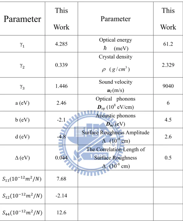
EV EC
Given a surface field Fs0
Then, initial V0(z)= Fs0* z Ehole
0
Six-band k・p Schrödinger Equation Solver with
Triangular Potential
1. DOS Mass <mv
DOS>
2. Quantization Mass mv
QN
EMA Oriented Schrodinger-Poisson Iteration Solver
with Fs ≈ Fs0
Through Eq. (1) and (2)
Ref. [4] As a Booster of Fully-iterated Six-band k・p Schrödinger – Poisson Self-consistent loop Applications Strained (001) & (110) p-MOSFETs Gate Direct Tunneling & CV fitting
Enhanced EMA Algorithm
Fig. 2.1The flowchart of our enhanced EMA algorithm. In the inserted
equations,
𝐸
1,𝑣is the first subband of the
𝑣th bulk band 𝐸
𝑣0, and
𝐷𝑂𝑆
1,𝑣(𝐸) is the density-of-states function for 𝐸
1,𝑣.
𝐹
𝑠is the surface
field,
𝑞 is the free electron charge, and 𝑓(𝐸) is the Fermi-Dirac
distribution.
26
Fig. 2.2 The device structures for (001) and (110) p-MOSFETs. The
channel direction and applied stress direction are clarified. Here, only the
favorable longitudinal compressive stress is under study.
Long. Comp.
Stress
n-typeW
L
(001) wafer
<110> channel
Long. Comp.
Stress
n-typeW
L
(110) wafer
<-110> channel
27 0.8 1.0 1.2 1.4 1.6 0.0 0.1 0.2 0.3 0.4 0.5 0.6 constant mass Long. -3 GPa Long. -1 GPa Long. -3 GPa Long. -1 GPa no stress
|V
s(V)|
Hole
Effec
tive Mass
(
m
0)
m
H1 QN<m
H1 DOS>
0.8 1.0 1.2 1.4 1.6 0.4 0.6 0.8 1.0 1.2 1.4 1.6 1.8 2.0 (001) p-MOSFET Temp. = 300 K ND= 1e17 cm-3 no stressFig. 2.4.1 The resulting (001) effective masses for H1 bulk band versus surface
bending. The heavy, light, and split-off holes, for each subband energy, are mixed
due to the coupling effect from the surface quantum confinement or the strain
effect [7]. Therefore, we group the subband energies mainly according to the three
lowest bulk bands,
𝐸
10(H1),
𝐸
28 0.8 1.0 1.2 1.4 1.6 0.0 0.1 0.2 0.3 0.4 0.5 0.6
|V
s(V)|
no stress 0.8 1.0 1.2 1.4 1.6 0.4 0.6 0.8 1.0 1.2 1.4 1.6 1.8 2.0 constant mass Long. -3 GPa Long. -1 GPa Long. -1 GPa Long. -3 GPaHole
Effec
tive Mass
(
m
0)
m
H2 QN<m
H2 DOS>
Long. -1 GPa no stressFig. 2.4.2 The resulting (001) effective masses for H2 bulk band. The orange
dashed lines refer to the constant effective masses as in unstressed conditions.
29 0.8 1.0 1.2 1.4 1.6 0.0 0.1 0.2 0.3 0.4 0.5 0.6
m
H3QN<m
H3DOS>
no stress 0.8 1.0 1.2 1.4 1.6 0.4 0.6 0.8 1.0 1.2 1.4 1.6 1.8 2.0 constant mass Long. -3 GPa Long. -1 GPa Long. -3 GPa Long. -1 GPa|V
s(V)|
Hole
Effec
tive Mass
(
m
0)
no stress30 0.8 1.0 1.2 1.4 1.6 1 2 3 4 5 6 7 8 9 10 (110) p-MOSFET Temp. = 300 K ND= 1e17 cm-3
m
H1QN<m
H1DOS>
no stress 0.8 1.0 1.2 1.4 1.6 0.0 0.1 0.2 0.3 0.4 0.5 0.6constant mass Long. -3 GPa
Long. -1 GPa Long. -3 GPa
|V
s(V)|
Hole E
ffec
tive Mas
s
(m
0)
no stress Long. -1 GPaFig. 2.4.4 The resulting (110) effective masses for H1 bulk band. Only H1 and
H2 bulk bands are shown in (110) case here because of their high occupation in
the subband energies. Note that (110)
𝑚
𝑄𝑁𝐻1is stress sensitive.
31 0.8 1.0 1.2 1.4 1.6 0.0 0.5 1.0 1.5 2.0 2.5 3.0 3.5 4.0 constant mass 0.8 1.0 1.2 1.4 1.6 0.0 0.1 0.2 0.3 0.4 0.5 0.6 Long. -3 GPa Long. -1 GPa no stress
|V
s(V)|
Hole
Effec
tive Mass
(
m
0)
m
H2QN<m
H2DOS>
Long. -3 GPa Long. -1 GPa no stress32 1.0 1.1 1.2 1.3 1.4 1.5 0.0 0.1 0.2 0.3 0.4 0.5 0.6 0.7 Fermi level Bulk band H1 Bulk band H2 Bulk band H3 Solid Lines = fully-iterated
Solid Symbols = eEMA
Open Symbols = constant EMA (001) w/o stress
V
S(V)
Sub
band
E
nergy (eV)
Fig. 2.4.6 The comparison of subband energy of (001) without stress among
fully-iterated, eEMA and constant EMA.
33 1.0 1.1 1.2 1.3 1.4 1.5 0.0 0.1 0.2 0.3 0.4 0.5 0.6 0.7 Fermi level Bulk band H1 Bulk band H2 Bulk band H3 Solid Lines = fully-iterated
Solid Symbols = eEMA
Open Symbols = constant EMA (001) Long. -1GPa
V
S(V)
Sub
band
E
nergy (eV)
Fig. 2.4.7 The comparison of subband energy of (001) under longitudinal
compressive stress 1 GPa among fully-iterated, eEMA and constant EMA.
34 1.0 1.1 1.2 1.3 1.4 -0.1 0.0 0.1 0.2 0.3 0.4 0.5 0.6 0.7 0.8 Fermi level Bulk band H1 Bulk band H2 Bulk band H3
Solid Lines = fully-iterated Solid Symbols = eEMA
Open Symbols = constant EMA (001) Long. -3 GPa
V
S(V)
Sub
band
E
nergy (eV)
Fig 2.4.8 The comparison of subband energy of (001) under longitudinal
compressive stress 3 GPa among fully-iterated, eEMA and constant EMA.
35 1.0 1.1 1.2 1.3 1.4 0.0 0.1 0.2 0.3 0.4 0.5 0.6 Fermi level Bulk band H1 Bulk band H2 Bulk band H3
Sub
band
E
nergy (eV)
Solid Lines = fully-iterated Solid Symbols = eEMA
Open Symbols = constant EMA (110) w/o stress
V
S(V)
Fig. 2.4.9 The comparison of subband energy of (110) without stress among
fully-iterated, eEMA and constant EMA.
36 1.0 1.1 1.2 1.3 0.0 0.1 0.2 0.3 0.4 0.5 0.6 Fermi level Bulk band H1 Bulk band H2 Bulk band H3
V
S(V)
Sub
band
E
nergy (eV)
Solid Lines = fully-iterated Solid Symbols = eEMA
Open Symbols = constant EMA (110) Long. -1GPa
Fig. 2.4.10 The comparison of subband energy of (110) under longitudinal
compressive stress 1 GPa among fully-iterated, eEMA and constant EMA.
37 0.8 0.9 1.0 1.1 1.2 -0.1 0.0 0.1 0.2 0.3 0.4 0.5 0.6 Fermi level Bulk band H1 Bulk band H2 Bulk band H3
Solid Lines = fully-iterated Solid Symbols = eEMA
Open Symbols = constant EMA (110) Long. -3 GPa
V
S(V)
Sub
band
E
nergy (eV)
Fig. 2.4.11 The comparison of subband energy of (110) under longitudinal
compressive stress 3 GPa among fully-iterated, eEMA and constant EMA.
38 -2 -1 0 1 2 0.0 0.4 0.8 1.2 1.6 2.0 (m0) mQN <mDOS> H1 0.27 1.13 H2 0.21 0.67 H3 0. 25 0.94
constant EMA with fully-iterated eEMA (001) p-MOSFET ND= 1e17 cm-3 Npoly= 1e20 cm-3 Tox= 1.9 nm
V
G(V)
Ca
pacitance
(
F/
cm
2)
Fig. 3.1.1 The comparison of calculated non-stress (001) gate capacitance
versus gate voltage from the constant EMA and enhanced EMA with the
sophisticated six-band k·p results.
39 -2 -1 0 1 2 0.0 0.4 0.8 1.2 1.6 2.0 2.4 (m0) mQN <mDOS> H1 0.59 0.12 H2 0.214 0.356 H3 0.212 0.248
constant EMA with fully-iterated eEMA (110) p-MOSFET ND= 1e17 cm-3 Npoly= 6.5e19 cm-3 Tox= 1.3 nm
V
G(V)
Ca
pacitance
(
F/
cm
2)
[6]Fig. 3.1.2 The comparison of calculated non-stress (110) gate capacitance
versus gate voltage from the constant EMA and enhanced EMA with the
sophisticated six-band k·p results.
40 0.0 -0.5 -1.0 -1.5 -2.0 -2.5 -3.0 10-2 10-1 100 101 102 103 eEMA Temp. = 300 K ND= 1e17 cm-3 Npoly= 6.5e19 cm-3 Tox = 1.3 nm moxh = 0.38 m0