國
立
交
通
大
學
物理研究所
博
士
論
文
氧化物金屬奈米線及其奈米線接點之電子傳輸特性
Electronic Transport
in Conducting Metal Oxide Nanowires and
through Their Nanowire Contacts
研 究 生:林永翰
氧化物金屬奈米線及其奈米線接點之電子傳輸特性
Electronic Transport
in Conducting Metal Oxide Nanowires and
through Their Nanowire Contacts
研 究 生:林永翰 Student:Yong-Han Lin
指導教授:林志忠 教授 Advisor:Prof. Juhn-Jong Lin
國 立 交 通 大 學
物 理 研 究 所
博 士 論 文
A Thesis
Submitted to Institute of Physics College of Science National Chiao Tung University in Partial Fulfillment of the Requirements
for the Degree of Doctor of Philosophy
in
Physics July 2007
Hsinchu, Taiwan, Republic of China
氧化物金屬奈米線及其奈米線接點之電子傳輸特性
學生:林永翰
指導教授:林志忠 教授
國立交通大學物理研究所博士班
摘
要
毫無疑問,瞭解電子在奈米線內部的運動行為是應用奈米線製作新穎
奈米電子元件一個相當重要的步驟,然而,要能實際達成應用的目的,
僅止於這樣的瞭解卻是不夠的。我們知道,任何奈米線,不論是作為
元件本身或是作為傳遞訊號的導線,它都必須與外界有所接觸,這個
接觸可能是元件與元件之間的連結,也可能是元件與巨觀世界之間的
連結。由於相關奈米製程的步驟繁複,一個非理想的接點顯然十分容
易因為污染或製程條件的些微差異而形成,而這樣一個非理想的接點
極可能會改變電子的運動方式,並進而影響元件的正常操作模式。因
此,徹底掌握電子在奈米線內部與在奈米線接點附近的傳輸特性是兩
個同等重要的研究課題。
本篇論文即是針對上述的主題,以 RuO
2與 IrO
2兩種極具應用價
值的氧化物金屬奈米線為主體,進行一完整的研究。RuO
2與 IrO
2是具
有相同結構、高度化學與熱穩定性,以及擁有相當於一般金屬導電率
的過渡金屬氧化物。利用標準的電子束微影製程,以及運用不同數目
的量測電極,我們不僅釐清了它們本身從室溫到液態氦溫度的電子傳
輸特性,也成功地描述了電子在奈米線接點附近從室溫到液態氦溫度
的運動行為。
關於 RuO
2與 IrO
2奈米線本身的電子傳輸特性,我們發現,與它
們的單晶塊材相同,其奈米線的電阻率從室溫到液態氦溫度的變化仍
舊可以用 Boltzmann 傳輸理論來成功描述。然而,對於 RuO
奈米線
縮小而大幅度的變小。對於直徑約 40 奈米的 RuO
2奈米線而言,其內
的 Debye 溫度已變小至只有其單晶塊材 Debye 溫度的大約一半大小。
對於我們所觀察到的結果,我們提出並探討了一些可能引發這種現象
的物理機制,我們歸納後認為,這樣的現象應該是來自於晶格點與晶
格點之間的等效鍵結力(亦即晶體的楊格彈性係數)隨著奈米線直徑變
小而減弱所導致。另外,在此篇論文裡,我們將僅報告較大直徑 IrO
2奈米線的測量結果,對於較小直徑 IrO
2奈米線的進一步測量則正在進
行當中。
對於電子通過 RuO
2與 IrO
2奈米線接點的傳輸行為,我們發現,
對於具有較高接觸電阻的接點而言,不同材質的奈米線,其接觸電阻
隨溫度變化的行為分別可以用不同的物理模型(函數關係)來成功解
釋。在 RuO
2奈米線方面,我們發現,其較高阻值的接觸電阻隨溫度
的變化行為可以用 thermally fluctuation-induced tunneling 的物理模型
來解釋,這主要是由於在接點附近形成一個等效的絕緣層,導致電子
通過接點時是以 tunneling 的方式來傳遞。在 IrO
2奈米線方面,我們發
現,在溫度約 100 K 以下,其較高阻值的接觸電阻與溫度的相依關係
則是遵從了 logR 正比於 T
-1/2的關係式,這主要是因為在接點附近形
成了一個由顆粒狀金屬所組成的區域,使得電子通過接點時是以
hopping 的方式來傳輸。我們認為,不同材質奈米線的接觸電阻具有
不同的溫度相依關係,極可能只是一個隨機的結果,亦即,接點結構
乃是從兩種可能的結構當中(絕緣層或顆粒層)隨機形成,然而,這樣
的結構差異也很可能是肇因於金屬電極材料(本篇論文使用 Cr/Au 作
為電極材料)在不同材質的奈米線上具有不同的表面應力。更進一步的
釐清我們則正在進行當中。
誌
謝
感謝我的父母
以及
Abstract
Fair understanding of the intrinsic electronic transport properties of individ-ual nanowires (NWs) is certainly the key step for numerous nanoelectronic applications. Quantitative knowledge about the relevant electronic contacts is also very crucial in correctly interpreting the experimental results. In this work, we have studied the intrinsic electronic transport properties of
indi-vidual single-crystalline RuO2 and IrO2 NWs, which belong to the family of
transition metal oxides that have advantages of being chemically stable while possessing comparatively high conductivities. With the help of the standard electron-beam lithographic technique, individual NWs are contacted by submi-cron metal electrodes from above. By applying different probe configurations to our measurements, not only the intrinsic electronic transport properties of the individual as-grown NWs but also the temperature behaviours of
high-resistance electronic contacts, Rc(T ), have been determined down to
liquid-helium temperatures.
Two main results have been obtained. First, the measured temperature dependent resistivity of the NWs is found to agree well with the current theo-retical understanding of these materials. Although they can be well described
by the existing theory, we found that the Debye temperature in RuO2 NWs
is significantly reduced to only one half of its bulk value when the diameter
of the NW decreases down to ≈ 40 nm. (Comparable experiments on IrO2
NWs with diameters down to this scale have not been performed.) Possible mechanisms accounting for this observation have been discussed. It is conjec-tured that the chemical binding in the NWs may be gradually weakened as the diameter decreases.
Second, for high-resistance electronic contacts, the measured Rc(T ) reveals
semiconducting or insulating behaviour, i.e., it increases rapidly with decreas-ing temperature. However, different temperature dependence has been found
for different kind of NW. For RuO2 NWs, the temperature behavior of Rc
can be satisfactorily explained in terms of the thermally fluctuation-induced tunneling through a junction formed at the interface between the electrode
and the NW. On the other hand, for IrO2 NWs, a power law of the form
logRc ∝ T−1/2 over a very wide temperature range from ≈ 100 K down to
liquid-helium temperatures has been observed. This later conduction process is ascribed to the hopping of electrons through nanoscale metal (Cr) granules incidentally formed at the contact region during the thermal evaporation of the submicron Cr/Au electrodes. Although such a difference may arise from the different surface conditions of different kinds of NWs (such as different surface stresses), we believe that either mechanism could occur even for the same kind of NW; they just appear randomly. Unfortunately, direct evidences supporting this viewpoint are not obtained in this work.
Contents
Abstract . . . ii
List of Tables . . . vi
List of Figures . . . vii
1 Introduction . . . 1 2 Experimental method . . . 5 2.1 Fabrication of nanowires . . . 5 2.1.1 RuO2 . . . 5 2.1.2 IrO2 . . . 8 2.2 Electrical measurements . . . 10
3 Electronic transport in metal nanowires . . . 16
3.1 Introduction . . . 16
3.2 Theoretical background . . . 16
3.3 RuO2 . . . 20
3.3.1 Nanowires with diameters ' 100 nm . . . 24
3.3.2 Nanowires with diameters < 100 nm . . . . 37
3.3.2.1 Size-dependent Debye temperature . . . 37
3.4 IrO2 . . . 46
4 Electronic transport through metal nanowire contacts . . . 51
4.1 Introduction . . . 51
4.2 RuO2 . . . 54
4.2.1 Fluctuation-induced tunneling conduction . . . 54
4.3.1 Electron hopping conduction . . . 60
5 Conclusion . . . 68
List of Tables
Table 3.1 Sample parameters for the eight RuO2 NWs measured by the
4-p method. Because the NWs have square cross sections, the diameter here means the side length of the square. The large uncertainties in length (defined as the length of the section that we actually probe) are mainly due to the large widths of the voltage probes and thus result in the large uncertainties
in resistivity. . . 22
Table 3.2 Values of the relevant parameters for the eight RuO2 NWs
measured by the 4-p method. . . 28
Table 3.3 Values of the relevant parameters for the two IrO2 NWs
mea-sured by the 4-p method. For both samples, W ≈ 180 ± 5 nm and L ≈ 0.83 ± 0.01 µm. The uncertainties in resistivities mainly arise from the uncertainties in the dimensions of the
NWs. . . 49
Table 4.1 Values of relevant parameters for four high-resistance NW devices, as determined from the 2-probe method. For each
device, the NW resistance Rs(300 K) was estimated from the
4-probe method, while the junction area A was determined
from the SEM image. . . 59
Table 4.2 Values of the relevant parameters for the three-probe and two-probe electrical measurement configurations implemented on the Ir-3 NW contacted by three submicron Cr/Au (10/90 nm) electrodes. The Ir-3 NW has a hypotenuse W ≈ 115 ± 5 nm,
length L ≈ 0.7 µm, and the sample resistance Rs(300 K) ≈ 0.5
List of Figures
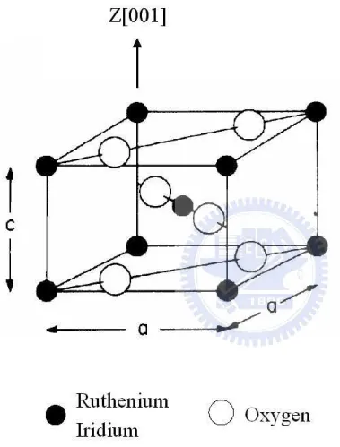
Figure 2.1 Rutile structure. . . 6
Figure 2.2 TEM image for a RuO2 NW. . . 7
Figure 2.3 (a) Tilted FESEM image of as-grown IrO2 NWs revealing nearly triangular cross sections. (b) Schematic plot of the geometry for a NW. (c) XRD pattern of the NWs. . . 9
Figure 2.4 Schematic plot of making electrical contacts onto individual NWs. . . 12
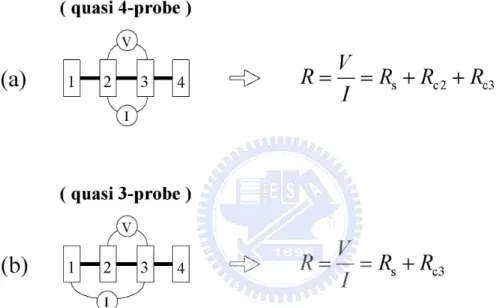
Figure 2.5 (a) Schematic diagram for a single NW (thick bar) with four electronic contacts on it and the equivalent circuit model. Rs denotes the resistance of each segment of the NW (i.e., the sample resistance). Rc1, Rc2, Rc3 and Rc4 denote the electronic contact resistances between the NW and the sub-micron electrodes 1, 2, 3 and 4, respectively. Rel,i denotes the submicron-electrode resistance of the ith electrode. Four-probe (b), three-Four-probe (c) and two-Four-probe (d) measurement configurations, and the corresponding measured resistances. In (d), the approximations Rc2 ≈ Rc3 ≡ Rc and Rel,2 ≈ Rel,3≡ Rel are assumed (see text). . . 13
Figure 2.6 Additional probe configurations needed to extract the resis-tance of each electronic contact. . . 15
Figure 3.1 Typical temperature behaviour of RuO2 NWs. . . 21
Figure 3.2 SEM image of the Ru-8 NW. . . 23
Figure 3.3 Variation of the resistivity at T = 300 K with diameter of the NW for the NWs measured in the present work. . . 25
Figure 3.4 log-log plot of the variation of the measured normalized resis-tivity, (ρ − ρ0)/ρ0, as a function of temperature for two NWs with diameters ≈ 100 nm. . . . 26
Figure 3.5 Variation of ΘD with diameter. . . 29
Figure 3.6 Variation of ΘE with diameter. . . 30
Figure 3.8 Variation of ρ0 with diameter. . . 32
Figure 3.9 Best fit for the sample Ru-4 by intentionally setting ΘD and
ΘEto their bulk values (i.e., 400 and 790 K, respectively) and
leaving only ρ0 and βBG as free variables. . . 33
Figure 3.10Best fit for the sample Ru-4 to the Eq. (3.10) by intentionally
setting ΘD and ΘE to their bulk values (i.e., 400 and 790 K,
respectively) and leaving only ρ0, βBG, and βintas free variables. 36
Figure 3.11Variation of βint with diameter. . . 38
Figure 3.12f (x) as a function of x for a material with a ΘD at several
different temperatures. . . 43
Figure 3.13Resistivity as a function of temperature for two IrO2 NWs
measured by the four-probe method. The symbols are the experimental data and the solid lines are the theoretical pre-dictions of equation (3.11). The inset shows the SEM image
of one NW contacted by four Cr/Au electrodes. . . 47
Figure 3.14Log-log plot of the variation of the normalized resistivity
∆ρ/ρ0 = (ρ − ρ0)/ρ0 with temperature for the two IrO2 NWs
studied in figure 3.13. Notice that the scales of the axes are
different in (a) and (b). The contribution from the ρint/ρ0
term in the Ir-1 NW has the same magnitude as that (∼ 10−3)
in the Ir-2 NW, and thus is outside the range displayed in (a). 50 Figure 4.1 Three typical temperature behaviours of the measured
resis-tance R, as determined from the 2-p method. . . . 53
Figure 4.2 Resistance as a function of temperature for two high-resistance contacts in series, as determined from the 2-probe method on the NW device C3 (see Table 4.1). The inset shows a plot of
logR versus T−1 for the same NW device. The straight solid
line indicates the thermal activation conduction. . . 55
Figure 4.3 Double logarithmic plot of the resistances versus temperature for four high-resistance NW devices, as determined from the 2-probe method. The symbols are the experimental data and
Figure 4.4 (a) Resistances as a function of temperature for the 2-probe and 3-probe measurement configurations as depicted in Figs. 2.5(c) and (d). The inset shows logR as a function of 1/T . (b)
logR as a function of T−1/2. Since R
2−p ≈ Rc2 + Rc3 and
R3−p ≈ Rc3, the difference between the two curves is simply
the electronic contact resistance Rc2. . . 62
Figure 4.5 (a) AFM image of a thin Cr layer with a mean thickness of 10 nm prepared by thermal-evaporation deposition on a mica substrate. (b) Surface profile along the line indicated in (a), showing a distribution of disk-shaped grains having radius of
Chapter 1
Introduction
Over the past decade, nanostructures have received much attention because they not only have great potential for novel industrial applications but also could provide a peculiar system for fundamental researches on issues about dimensionality and space-confined phenomena. Among the various nanostruc-tures, self-assembled quasi-one-dimensional (Q1D) metallic nanowires (NWs) are of particular interest due to their promising applicability in the future nano-electronics as elemental devices or as probes that diagnose functional circuitry. For instance, the molecular carbon nanotubes (CNTs) are shown to behave (in some cases) ballistically and be capable of sustaining extremely high cur-rent densities [1]. Prototypical nanoelectronic devices based on a single CNT have been proposed and tested [2]. To date, in addition to the extensively studied CNTs [1, 2], great amounts of efforts have been focusing on quasi-one-dimensional semiconductors [3] and their binary compounds including Si [4], ZnO [5], GaN [6], etc.
Of course, for all fascinating applications to be true, fair understanding of the intrinsic electronic transport properties of these Q1D metallic NWs is the very first and key step for the realization of numerous possibilities. How-ever, although nowadays various metallic NW systems have been successfully synthesized, electrical characterizations on individual metallic NWs have been comparatively less reported with only very few exceptions like metallic silicide [7] and semi-metallic Bi [8, 9]. This lack of reports mainly originates from the problem of uncontrollable surface oxidation that largely hinders reliable electrical measurements from being taken [8]. Measurements so far were thus mostly performed simultaneously on a great number of NWs imbedded in an insulating porous template, by using the simple 2-probe method. In that way, the influences of the contacts apparently cannot be explicitly excluded and the
unique properties of individual NWs could also be easily smeared out.
In this context, conducting metal oxides, such as RuO2 and IrO2, that
have advantages of being chemically stable while possessing comparatively high conductivities, can thus provide an alternative and excellent choice for nanodevice-related applications and most of all, fundamental electronic trans-port studies, from which the information inferred over a wide range of temper-ature (and, further, with the application of magnetic fields) will help clarify the electronic conduction mechanism in metal and semiconductor NWs.
Recently, syntheses of single-crystalline RuO2 and IrO2 NWs have been
reported by means of different techniques including cryogenic decomposition [10], metal-organic chemical vapor deposition [11], reactive sputtering [12], and many others [13, 14, 15]. Nevertheless, despite the fact that they are metallic oxides with superior chemical stabilities, the intrinsic temperature dependent electronic transport properties of these highly applicable materials down to the nanoscale have not yet been fully characterized so far.
This fact may result from another frequently encountered technical diffi-culty. Since exploring the electronic transport properties in these Q1D systems requires the connections of the instruments to the individual nanostructures, nanofabrication techniques such as the electron-beam lithography (EBL) and the focused ion beam deposition are usually employed to accomplish this need. However, it is known that fabrication of reliable electronic contacts to the nan-odevices has been a nontrivial issue, because very often an imperfect contact inevitably forms and may possess a non-negligible temperature dependent
con-tact resistance, Rc(T ), which in turn is prone to complicate the experiments
and could seriously mislead the physical interpretation of the data. The
high-resistance Rc may be as a result of the surface contamination of the NW,
or the minor break of the electrode at the contact where it just touches the NW. Either could be easily introduced due to the complexity of the whole fabrication process.
From the physical point of view, in the cases involving semiconductors, the contact between a metal electrode and a semiconductor NW usually forms a Schottky barrier, whose properties have been extensively studied [16]. A
different situation concerning heavily doped semiconductor NW has also been discussed [17]. On the contrary, the electrical properties of the contact between a metal electrode and a metal NW have not yet been much addressed in the literature. In the case of metal NWs, since the NWs may readily be separated from the electrode by a layer of some insulator (oxidation, contamination, an amorphous coating, or a break, etc.) of a few nm thick, the underlying physics of how electron waves transmit through such a nanoscale interface should be of fundamental interest and urgent industrial concerns.
In this work, we report the electronic transport measurements on
individ-ual single-crystalline RuO2 and IrO2 NWs fabricated by the thermal
evapora-tion method and the metal-organic chemical vapor deposievapora-tion method, respec-tively. With the help of the EBL technique, individual NWs were contacted by submicron electrodes from above. Utilizing different probe configurations in our measurements, not only the intrinsic electronic transport properties of individual NWs but also the temperature dependent high-resistance electronic contacts (which incidentally formed at the interfaces between the lithographic-patterned submicron electrodes and the NWs) have been determined from 300 K down to liquid-helium temperatures.
We found that the electronic transport properties of our as-grown NWs can be explained in terms of the current theoretical understanding for these ma-terials. The measured temperature dependent resistivities are well accounted
for by the scattering of electrons with phonons. However, for RuO2 NWs with
diameters of several tens nm, the effective Debye temperature was found to be
largely reduced as compared with its bulk value.1 It is conjectured that the
chemical binding of the lattice may be weakened as the diameter of the NW decreases.
On the other hand, instead of providing a solution to the problem resulting
in the high-resistance Rc, we demonstrated that the temperature behavior of
Rc, however, can be well understood in terms of two existing phenomenological
1Investigations of the IrO
2NWs with diameters down to the similar scales have not been
performed yet because of the experimental difficulty of patterning four submicron electrodes onto such NWs, of which the lengths are rather shorter than those of the RuO2 NWs.
theories, one for RuO2NWs, and one for IrO2NWs. Although such a difference
may arise from the different surface conditions of different kinds of NWs (such as different surface stresses), we believe that either mechanism could occur even for the same kind of NWs; they just appear randomly. Unfortunately, direct evidences supporting this viewpoint are not obtained in this work.
To our knowledge, the present work is the first quantitative electrical char-acterization on these highly applicable materials down to the nanoscale, and also over such a wide range of temperature.
Chapter 2
Experimental method
2.1
Fabrication of nanowires
The NWs used in the present work are provided by Profs. Fu-Rong Chen and Ji-Jung Kai’s group at the Department of Engineering and System Science
of National Tsing Hua University (RuO2) and by Prof. Ying-Sheng Huang’s
group at the Department of Electronic Engineering of National Taiwan
Uni-versity of Science and Technology (IrO2). The fabrication processes are briefly
given here. Detailed descriptions of fabrication processes and other material characterizations for each kind of NWs can be found in the references as indi-cated in the text.
2.1.1
RuO
2Ruthenium dioxide, RuO2, together with several other oxides, such as IrO2 and
OsO2, crystallizes in the rutile structure (Fig. 2.1) and belongs to the family
of transition metal oxides that exhibit metallic conductivities comparable with those of the parent metals themselves [18, 19]. Owing to its excellent thermal and chemical stability [20, 21], it has been investigated for applications in many diverse fields. For example, it has been used as resistive thermometers in cryogenics [22], as corrosion-resistant low-overpotential electrodes for chlorine and oxygen evolution in electrolysis [23], and as electrochemical capacitors for energy storage in power industry [24]. Moreover, in addition to being an strip-line conductor [25] and an electrical contact material [26] in vast electronics,
RuO2 as well finds its application in modern very large scale integrated circuits
as an outstanding diffusion barrier between Al and Si in contact metallizations [27].
evaporation method based on the vapor-liquid-solid growth mechanism,[28] using Au nanoparticles (Ted-pella, 5–40 nm in diameter) as catalyst. A con-ventional quartz tube furnace was used for the synthesis. The tube was first
cleaned by evacuating it to a base pressure of 10−3 torr. Oxygen gas (99.9%)
was then introduced as a carrier gas to transport the vapor produced by
evap-orating stoichiometric RuO2 powder (Aldrich, 99.9%), which was placed in the
tube center, at 920–960◦C. The pressure and the flow rate of the carrier gas
was 2 torr and 100 sccm, respectively. Silicon substrates with a native oxide layer on top were placed at the downstream end of the tube, where the
temper-ature was kept at 450–670◦C. Several hours later, single-crystalline RuO
2 NWs
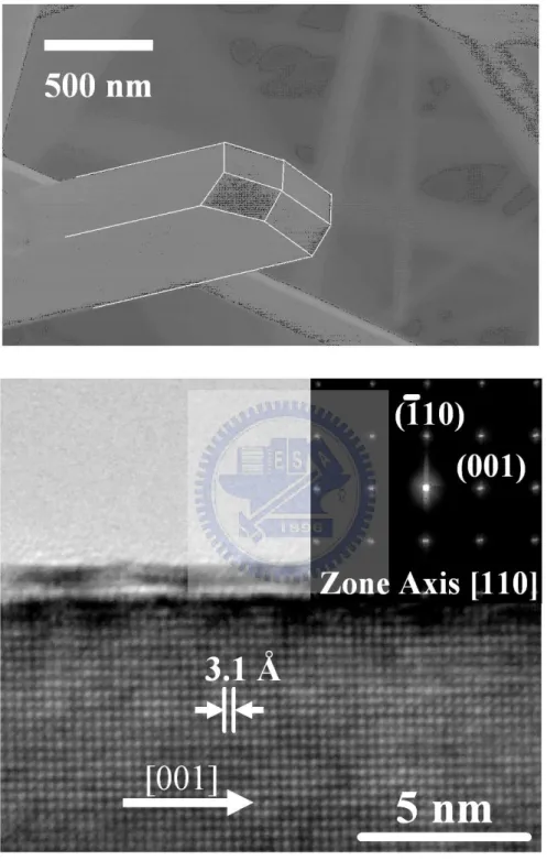
were grown on the substrates. The as-deposited NWs were further analyzed by using field-emission scanning electron microscopy (FE-SEM), transmission electron microscopy (TEM), x-ray diffraction (XRD), and x-ray energy disper-sive spectroscopy (XR-EDS). Figure 2.2(a) shows the SEM image focused on a particular NW, of which the nearly square cross section is illustrated. The TEM image and the corresponding electron diffraction pattern are shown in Fig. 2.2(b). Detailed results of the material characterizations can be found elsewhere [15].
2.1.2
IrO
2Iridium dioxide, IrO2, also crystallizes in the rutile structure with the lattice
constants differing from RuO2 by less than ≈ 1 % (see Fig. 2.1). Owing to its
high resistance to the inter-diffusion of oxygen, as well as its excellent thermal and chemical stability [29], it has been used in many diverse applications. For instance, it has been investigated for use as optical switches in electrochromic devices [30], as thin film electrodes for dynamic random access memories [31], and as durable electrode materials for oxygen or chlorine evolution [32]. More
recently, IrO2 NWs have been studied as high-performance and robust field
emitters due to their low surface work function [33].
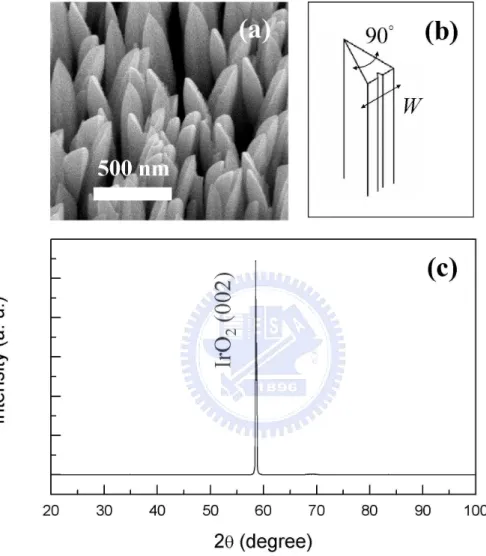
Self-assembled single-crystalline IrO2 NWs were grown onto sapphire (100)
Figure 2.3: (a) Tilted FESEM image of as-grown IrO2 NWs revealing nearly
triangular cross sections. (b) Schematic plot of the geometry for a NW. (c) XRD pattern of the NWs.
reagent (MeCp)Ir(COD) supplied by the Strem Chemicals. Both the pre-cursor reservoir and the transport line were controlled in the temperature
range of 100−130◦C to avoid precursor condensation during the vapor-phase
transport. High purity oxygen, with a flow rate of 100 sccm, was used as the carrier gas and reactive gas. During the deposition, the substrate
tempera-ture was kept at 350◦C, and the chamber pressure was held at 23±1 mbar to
obtain the quasi-one-dimensional IrO2 crystals. The deposition rate of NWs
with nearly triangular cross sections was estimated to be 20–25 nm/min. By adjusting the temperatures of precursor reservoir and substrate, NWs with different cross-sectional morphologies, such as triangles and squares, could be obtained [34]. For the sake of convenience for resistance measurements, the NWs with nearly triangular cross sections [figures 2.3(a) and 2.3(b)] were used in this work since they have the longest length (∼ 3 µm) among all morpholo-gies. The as-deposited NWs were analyzed using field-emission scanning elec-tron microscopy (FE-SEM), transmission elecelec-tron microscopy (TEM), x-ray diffraction (XRD) and x-ray photoelectron spectroscopy (XPS). Figure 2.3(c) shows the XRD pattern of the NWs used in this work, in which the unique (002) diffraction signal indicates the nearly single-crystalline quality as ob-tained in our previous results [35]. Detailed fabrication processes and material characterizations can be found elsewhere [33, 34, 35].
2.2
Electrical measurements
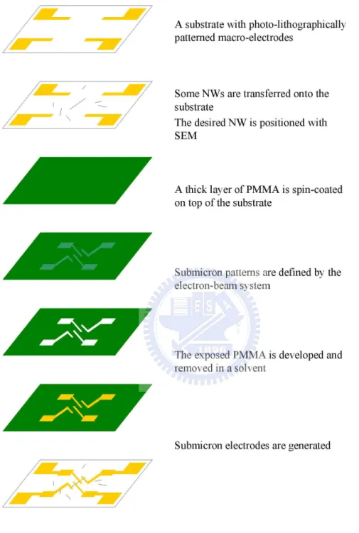
Electrical contacts onto individual NWs were fabricated by the standard EBL process as described below. Figure 2.4 shows the schematic plot of the
pro-cess. Silicon substrates with a ≈ 200-nm thick SiO2 layer on top were first
photo-lithographically patterned with Cr/Au (≈ 10/60 nm) macro-electrodes using bi-layer photoresist process to create reverse-slope resist sidewall profiles.
Several droplets of dispersed alcoholic solution containing RuO2 or IrO2 NWs
were dropped on the substrate. Transfer of the NWs could also be achieved by bringing the patterned Si substrate into loose surface contact with the substrate where the NWs were actually grown onto. No differences have been
found between these two methods.1 Individual NWs were then positioned with
SEM. A spin-coated thick layer of PMMA (polymethyl methacrylate) on top of the substrate was exposed to electron beam to produce submicron patterns. Following the thermal evaporation of Cr/Au films (≈ 10/90 nm thickness, ≈
1/5 ˚A/s deposition rate), lift-off techniques were applied to generate submicron
electrodes contacting the NWs.
Copper leads were attached to the macro-electrodes with Ag paste, and the substrate was thermally anchored to the sample holder mounted with a
calibrated silicon diode thermometer on a standard4He cryostat. For
measure-ments down to sub-Kelvin temperatures, an Oxford Heliox 3He refrigerator
with a calibrated RuO2 thermometer was used.
The resistances were measured by two different methods, depending on which measurement configuration was employed. First, in order to investigate the intrinsic electronic properties of individual NWs, a standard four-probe (4-p) measurement configuration [Fig. 2.5(b)] was applied, using a Linear Re-search LR-700 AC resistance bridge. Second, for the three-probe (3-p) and two-probe (2-p) measurement configurations [Fig. 2.5(c) and (d), respectively], the resistances were measured by the DC method, in which a Keithley K-6430 source meter as a current source and a K-182 nanovoltmeter were used, and the current-reversal method [36] was adopted so that any existing thermoelectric voltages along the measurement loop were canceled. For some 2-p measure-ments (in which higher resistance readings were obtained), only the K-6430 source meter was used.
Obviously, in the 2-p method, the measured resistance R is the sum of the
NW sample resistance Rs plus the two electronic contact resistances Rc’s and
the two submicron-electrode resistances Rel’s, i.e., R(T ) = Rs(T ) + 2Rc(T ) +
2Rel(T ). The prefactor 2 is introduced to denote that there are two similar
electronic contacts in series (and also, two similar submicron electrodes in
se-ries).2 We have assumed this simple case here because they were fabricated
1For IrO
2NWs, only the first method was used, i.e., the wet method.
2The resistances of the submicron electrodes are similar at least within an order of
Figure 2.4: Schematic plot of making electrical contacts onto individual NWs.
Figure 2.5: (a) Schematic diagram for a single NW (thick bar) with four
electronic contacts on it and the equivalent circuit model. Rs denotes the
resistance of each segment of the NW (i.e., the sample resistance). Rc1, Rc2,
Rc3 and Rc4 denote the electronic contact resistances between the NW and the
submicron electrodes 1, 2, 3 and 4, respectively. Rel,i denotes the
submicron-electrode resistance of the ith submicron-electrode. Four-probe (b), three-probe (c) and two-probe (d) measurement configurations, and the corresponding measured
resistances. In (d), the approximations Rc2≈ Rc3≡ Rcand Rel,2 ≈ Rel,3 ≡ Rel
simultaneously under the same condition and on the same NW. In the case
of high-resistance electronic contacts (i.e., R À Rs and R À Rel), the Rc
may dominate the measured resistance and the approximation R ≈ 2Rc is
valid for the whole range of experimental temperature. The measured magni-tude and temperature behavior of R thus faithfully reflect the magnimagni-tude and
temperature behavior of Rc. As a result, Rc(T ) can be quantitatively inferred.
For the case of low-resistance electronic contacts (i.e., Rc, Rs, and Rel are
similar within an order of magnitude), measurements using additional probe configurations are required to extract the resistance of each electronic contact.
For example, the resistance of the sum of the two electronic contacts Rc2
and Rc3 in Fig. 2.5 can be obtained by subtracting the 4-p result from the
result obtained from the quasi 4-p measurement configuration [Fig. 2.6(a)]. To further explicitly extract the resistance of each electronic contact, a quasi 3-p probe measurement configuration [Fig. 2.6(b)] is needed.
In the present work, only the cases of high-resistance electronic contacts are discussed.
Figure 2.6: Additional probe configurations needed to extract the resistance of each electronic contact.
Chapter 3
Electronic transport in metal nanowires
3.1
Introduction
Fundamental studies concerning the physical properties (e.g., electronic
struc-tures, Boltzmann transport properties, and optical properties) of RuO2 and
IrO2 have been investigated for a long time, both experimentally [18, 19, 37,
38, 39, 40] and theoretically [41, 42, 43, 44, 45]. It is often accepted that the current understanding of the material is fairly complete. In particular, the
electrical resistivities of RuO2 and IrO2 single crystals [18, 19] and disordered
thick films [46, 47, 48] have been investigated over a wide range of
tempera-ture from 0.3 up to 1000 K. It has been shown that, for RuO2 and IrO2 single
crystals, the temperature dependence of resistivity is essentially independent of the crystal orientation [18]. More specifically, the electronic conduction
pro-cess in RuO2 rutile has been theoretically determined from the first-principles
electronic-structure calculations and found to conform to the behavior as de-scribed by the Boltzmann transport equation [43]. Good agreement with the experiments has been established [19, 43].
3.2
Theoretical background
In this section, a brief description of the electronic transport properties of
RuO2 and IrO2 single crystals is given. More theoretical and experimental
details can be found in Refs. [19, 43].
Originally, the temperature dependent resistivities of RuO2 and IrO2 rutile
structures were explained [18] in terms of a tow-band model [49], which de-scribes the electron-phonon scattering in transition metals with parabolic s and
d bands. In this model, the electrons are scattered by acoustic phonons from
high band mass. However, based on their first-principles electronic-structure calculations, Glassford and Chelikowsky [43] have pointed out that the Fermi
surface of RuO2 has no such topology, which would account for such a high
degree of interband transitions between Fermi sheets. On the contrary, they
gave a description of the temperature behaviour of resistivity for RuO2 by
including an additional contribution due to the scattering of electrons with optical-mode phonons. It has been found to agree well with the experiments [19, 43].
Theoretically, the resistivity is defined as
ρ = 4π
Ω2
pτ
, (3.1)
where Ωp is the plasma frequency and 1/τ is the electron scattering rate. The
Ωp can be theoretically calculated from a knowledge of the electronic
struc-ture of the material or experimentally determined from optical and transport measurements. If only electron-phonon scattering is taken into account, the scattering rate 1/τ can be written as
1 τ ∝ Z ∞ 0 dω ω α 2F (ω) · ~w/2kBT sinh(~ω/2kBT ) ¸2 , (3.2)
where ω is the phonon frequency, α2 is the effective frequency dependent
electron-phonon coupling parameter, and F (ω) is the phonon density of states, which can be obtained from neutron scattering data. However, no matter
experimentally or theoretically, the so called “spectral function” α2F (ω) is
difficult to get separated and normally has to be considered as a whole. For typical metals, a Bloch-Gr¨uneisen type behaviour which accounts for the scattering of electrons with acoustic-mode phonons is followed. This model
can be obtained by replacing the α2F (ω) with its equivalent in the Debye
approximation (where F (ω) ∝ ω2 is assumed):
α2F (ω) ∝ λBG µ ω ωD ¶4 θ(ωD− ω) , (3.3)
where θ is the step function, ωD is the Debye frequency (which is defined as
coupling constant in the Bloch-Gr¨uneisen model. Substituting Eq. (3.3) into
Eq. (3.2) and letting x = ~ω/kBT , from Eq. (3.1) we have
ρBG(T ) = βBGT µ T ΘD ¶4Z ΘD/T 0 x5dx (ex− 1)(1 − e−x) , (3.4)
where βBG is a material dependent constant containing the information about
λBG and Ωp, and ΘD is the Debye temperature corresponding to the
max-imum phonon energy in the Debye approximation of the phonon spectrum
(i.e., ΘD = ~ωD/kB). At higher temperatures, Eq. (3.4) results in a
temper-ature dependence which is proportional to T , while at lower tempertemper-atures, it
gives a T5 dependence.
For transition-metal oxides which contain multi-atom bases that can de-velop extra branches of lattice vibrations, the scattering of electrons with such
optical-mode phonons should be considered as well. (In fact, for RuO2, there
exist 15 possible optical branches that the electrons can scatter from.) The contribution due to this scattering process can be obtained by replacing the
α2F (ω) with its equivalent in the Einstein approximation (where F (w) is a
delta function centered at the Einstein frequency ωE):
α2F (ω) ∝ λ
EωEδ(ω − ωE) , (3.5)
where δ is the delta function, and λEis the transport electron-phonon coupling
constant in the Einstein model. Substituting Eq. (3.5) into Eq. (3.2), from Eq. (3.1) we have ρE(T ) = βET · ΘE/2T sinh(ΘE/2T ) ¸2 , (3.6)
where where βE is a material dependent constant containing the information
about λE and Ωp, and ΘE is the Einstein temperature representing the sole
phonon energy in the Einstein approximation of the phonon spectrum (i.e.,
ΘE= ~ωE/kB).
Apart from the electron-phonon scattering, there is an additional term that could contribute to the temperature dependent resistivity. This is the usual
electron-electron scattering which depends on T2. It can be simply written as
where Aee is a material dependent constant.
According to Matthiessen’s rule, these three contributions [i.e., Eq. (3.4)– (3.7)] are additive and independent of each other. The total resistivity ρ(T )
is thus the sum of the residual resistivity ρ0 and Eqs. (3.4)–(3.7), i.e.,
ρ(T ) = ρ0+ ρBG(T ) + ρE(T ) + ρee(T ) . (3.8)
The measured resistivity can then be fitted to Eq. (3.8), in which ρ0, ΘD, βBG,
ΘE, βE, and Aee are normally regarded as adjusting parameters.
However, with so many fitting parameters, ambiguous results might occa-sionally occur. Fortunately, at not too high temperatures (e.g., at
tempera-tures below 300 K)1, the resistivity due to the usual electron-electron scattering
can be neglected in the first approximation because in practice in transition
metals Aee is only of the order of 10−5 K−2 µΩ cm [49]. Indeed, it has been
shown [19] that in RuO2 single crystals fitting the experimental data without
this term leads to only minor deviations of the remaining parameters (i.e.,
ΘD, βBG, ΘE, and βE) from those obtained by considering all the three
contri-butions. This conclusion has also been established in other transition metals [50]. On the other hand, since in the previous studies [19, 43] the ratio of the
values of βBG/βE, which determines the relative strength of the coupling of
electrons with acoustic- and optical-mode phonons, was found to be ≈ 2, we further assume this value in our following analysis to reduce the number of the adjusting parameters so that the more reliable results could be obtained. Nev-ertheless, it should be noted that to our knowledge the physics of the disorder dependence of this relative strength is still not clear yet.
To sum up, in the following analysis, the measured ρ(T ) of our NWs would be fitted to the equation
ρ(T ) = ρ0+ ρBG(T ) + ρE(T ) , (3.9)
in which only ρ0, ΘD, βBG, and ΘE are treated as adjusting parameters.
1According to their mathematical expressions, the electron-electron scattering could
dominate over the other two scattering processes at temperatures below liquid-helium tem-peratures. Physically, this is due to the much smaller number of excited phonons because of the low-temperature (i.e., low-energy) environment.
3.3
RuO
2To study the intrinsic electronic transport properties of our single-crystalline
RuO2 NWs, the resistivities ρ as a function of temperature from 300 K down
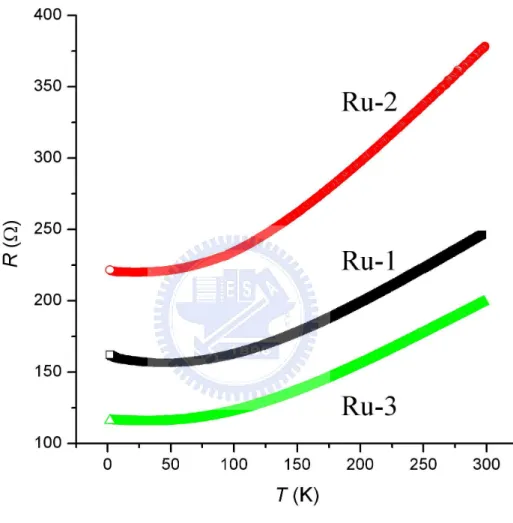
to liquid-helium temperatures for eight individual as-grown NWs were deter-mined with the 4-p measurement configuration. Typical behaviour of ρ(T ) is
shown in Fig. 3.1. The physical dimensions (inspected by SEM)2 and the room
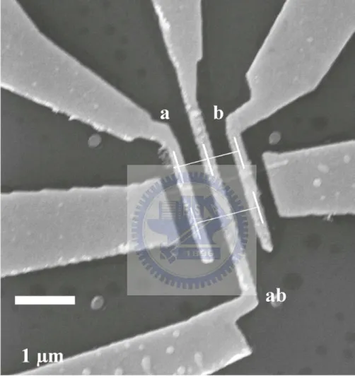
temperature resistivities of these NWs are listed in Table 3.1. Notice that the samples Ru-8a and Ru-8b are actually two different sections of the same NW, while the sample Ru-8ab is the sum of these two sections (see Fig. 3.2).
Clearly, the NWs reveal the electronic transport characteristic of a typ-ical metal, i.e., the resistivity decreases as the temperature decreases from room temperature down. However, the resistivity reaches a minimum value
(≡ ρmin) at a certain low temperature Tmin, below which it shows different
lev-els of upturn for different NWs. This notable resistance rise with decreasing temperature may originate from the weak-localization and electron-electron interaction effects [51] and two-level systems [52].
Figure 3.3 shows the variation of the resistivity at T = 300 K (≡ ρ300)
with diameter of the NW for the NWs measured in this work. Obviously, the
plausible ρ300 should be ≈ 150–300 µΩ cm, as obtained in 1, 4, and
Ru-5 (whose lengths are long enough to avoid the ambiguity of the determination of the length of the NW section that we actually probed). Nevertheless, this value is still considerably higher than that (≈ 85 ± 35 µΩ cm) in bulk single
crystals [18, 19]. Using the lowest measured ρ300 ≈ 150 µΩ cm and the relevant
material parameters for RuO2 [43], we extract in our NWs the electron mean
free path l ≈ 8.4 ˚A and the electron mean free time τ ≈ 3 × 10⁻¹⁵ s at 300 K.
Since this l is much shorter than the diameters of our NWs, an electron will on average have undergone several tens to few hundreds collisions (depending on
the diameter and the actual ρ300 of the NW) within the NW before it scatters
once off the NW surface. This diffusive motion of an electron implies that the
2To have more accurate values of the diameters, atomic force microscopy (AFM) was
Table 3.1: Sample parameters for the eight RuO2 NWs measured by the
4-p method. Because the NWs have square cross sections, the diameter here means the side length of the square. The large uncertainties in length (defined as the length of the section that we actually probe) are mainly due to the large widths of the voltage probes and thus result in the large uncertainties in resistivity.
Diameter Length ρ300 Tmin ρ300/ρmin
(nm) (µm) (µΩ cm) (K) Ru-1 155 ± 5 4.279 ± 0.984 149 ± 43 ≈ 45 1.588 Ru-2 135 ± 20 1.613 ± 0.882 724 ± 523 ≈ 22 1.725 Ru-3 110 ± 4 1.297 ± 0.842 339 ± 234 ≈ 32 1.742 Ru-4 104 ± 12 3.252 ± 0.790 281 ± 125 ≈ 42 1.685 Ru-5 97 ± 13 9.157 ± 0.704 184 ± 61 ≈ 43.5 1.561 Ru-6 76 ± 7 1.593 ± 0.862 825 ± 543 ≈ 53 1.435 Ru-7 55 ± 5 0.670 ± 0.441 483 ± 362 ≈ 27 1.609 Ru-8a 37 ± 2 0.516 ± 0.226 183 ± 95 < 10 1.536 Ru-8b 37 ± 2 0.516 ± 0.226 158 ± 82 < 10 1.579 Ru-8ab 37 ± 2 1.032 ± 0.226 141 ± 45 < 10 1.554
electronic transport properties in our NWs should be largely determined by their bulk properties while the surface effects may not be very effectual.
The residual resistivity ratio (RRR) ρ300/ρ0 ≡ ρ300/ρmin ≈ 1.5–1.7 for these
NWs are found to be significantly lower, as compared with the corresponding bulk value (≈ 100–1000, depending on the quality of the crystal) [18, 19]. Such properties as the low RRR values and the short l lengths all indicate the presence of a high level of defects (most likely, point defects) in the NWs. This observation is in sharp distinction to the conclusion drawn from conven-tional materials characterization techniques such as XRD and high-resolution TEM [15], which often reveal very high quality atomic structure. Similar phe-nomenon had also been found in single-crystalline metallic NiSi NWs [7]. This observation suggests that the electronic transport measurements over a wide range of temperature can serve as a powerful probe for investigating the physics concerning the microscopic defects in nanostructures because of its sensitivity to the microscopic motions of conduction electrons with the existence of any level of randomness in the crystal.
3.3.1
Nanowires with diameters ' 100 nm
Despite the disorder nature of our NWs, we found that for the temperature
behaviour above Tmin our experimental data still can be explained within the
framework of the Boltzmann transport theory for typical metals, as given in Section 3.2.
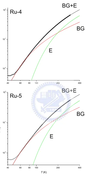
Figure 3.4 shows the log-log plot of the variation of the measured
normal-ized resistivity, (ρ − ρ0)/ρ0, as a function of temperature for two NWs with
diameters ≈ 100 nm. The solid line is the least-squares fit to Eq. (3.9). As
mentioned, we merely took ρ0, ΘD, βBG, and ΘE as adjusting parameters in
Figure 3.3: Variation of the resistivity at T = 300 K with diameter of the NW for the NWs measured in the present work.
40 60 80 100 200 400 10 -2 10 -1 10 0 40 60 80 100 200 400 10 -2 10 -1 10 0 E BG E BG BG+E BG+E Ru-5 Ru-4 / 0 T (K)
Figure 3.4: log-log plot of the variation of the measured normalized
Table 3.2. Figures 3.5–3.8 show the variations of ΘD, ΘE, βBG/ρ0,3 and ρ0
with diameter, respectively. In this section, only NWs with diameters ' 100 nm would be discussed. The results for NWs with diameters < 100 nm would be discussed later.
We first notice that the fitted values of ΘD and ΘE are nearly identical
for the NWs with diameters ' 100 nm. However, in comparison with the
corresponding bulk values (ΘD ≈ 400–410 K and ΘE ≈ 790–810 K) in single
crystals [19, 43], we find that the ΘD has a value of ≈ 400 ± 25 K, while the
ΘE has a value of ≈ 700 ± 25 K. A reduction of ≈ 13 % in ΘE is observed.
If we additionally set ΘD and ΘE to their bulk values (i.e., 400 and 790 K,
respectively) and left only ρ0 and βBG as free variables, we found that for all
the NWs no satisfactory results could be obtained as expected. A typical best fit in this way is shown in Fig. 3.9 for the sample Ru-4.
At first glance, since we are dealing with NWs, one might conjecture that this reduction in the effective phonon characteristic temperatures results from the increased electron scattering rate with surface phonons, which are softer than bulk phonons due to the lowered coordination number of surface atoms leading to their enhanced vibrational amplitudes. Nevertheless, in our case, as mentioned above, this electron-surface scattering is less effectual, because in our NWs, the much shorter electron mean free path as compared with the diameter of the NWs makes this process much infrequent. As a matter of fact, a change in phonon related properties such as these characteristic temperatures could also be induced by some structural [53, 54], compositional [55, 56], and mechanical [57, 58] effects. For instance, in thin gold films the lowering of the effective Debye temperature is ascribed due to the electron scattering with additional surfaces created by grain boundaries [53]. However,
3In fact, the measured resistance R was fitted to the equation of the form:
R − R0 R0 = ρ − ρ0 ρ0 = βBG ρ0 f (ΘD, ΘE) ,
where R0 is the residual resistance, and f is a function of ΘD and ΘE, obtained from
Eqs. (3.4) and (3.6). Therefore, the actual adjusting parameters are R0, βBG/ρ0, ΘD, and
Table 3.2: Values of the relevant parameters for the eight RuO2 NWs
mea-sured by the 4-p method.
Fit range ρ0 ΘD (βBG/ρ0) ΘE ρ300/ρ0 (K) (µΩ cm) (K) (10−3/K) (K) Ru-1 55–300 93 ± 27 426 ± 15 3.66 ± 0.04 726 ± 13 1.595 Ru-2 30–300 420 ± 303 365 ± 4 4.30 ± 0.01 689 ± 4 1.725 Ru-3 40–300 194 ± 134 372 ± 5 4.42 ± 0.02 687 ± 4 1.746 Ru-4 50–300 166 ± 74 377 ± 22 4.07 ± 0.06 674 ± 16 1.695 Ru-5 55-300 117 ± 39 373 ± 19 3.39 ± 0.04 690 ± 12 1.571 Ru-6 70–300 569 ± 375 393 ± 22 2.66 ± 0.03 672 ± 8 1.449 Ru-7 35–300 300 ± 225 324 ± 7 3.58 ± 0.02 692 ± 5 1.611 Ru-8a 30–300 119 ± 62 213 ± 13 3.07 ± 0.01 682 ± 2 1.532 Ru-8b 30–300 100 ± 52 234 ± 14 3.21 ± 0.02 617 ± 2 1.585 Ru-8ab 30–300 92 ± 29 229 ± 15 3.11 ± 0.01 660 ± 1 1.542
50 100 150 200 250 300 350 0.0 0.1 0.2 0.3 0.4 0.5 0.6 0.7 0.8 40 60 80 100 200 400 10 -2 10 -1 10 0 E E BG BG BG+E BG+E / 0 T (K)
Figure 3.9: Best fit for the sample Ru-4 by intentionally setting ΘD and ΘE
apart from being caused by these effects, we found that in the present work
another possibility could also account for the observed reduction in ΘE owing
to the simple fact that, in our moderately disordered NWs, we interpreted the resistivity variations as arising solely from the “pure” electron-phonon scattering process that usually dominate in clean metals.
Experimentally, it has been known for a long time that deviations from Matthiessen’s rule exist in many real metals. That is, the additivity and in-dependence which bring about Eq. (3.8) are no longer valid as the level of disorder in a metal increases. Recently, it becomes clear that such a devia-tion in an impure metal can be readily accounted for by merely adding an additional term into Eq. (3.8). This additional contribution was theoretically proposed and calculated by Reizer and Sergeev [59] as a consequence of the quantum interference mechanism between the elastic electron scattering and the electron-phonon scattering. It can be written as
ρint(T ) = βintρ0T2 Z ΘD/T 0 · x2ex (ex− 1)2 − x ex− 1 ¸ dx , (3.10)
where βint is a material dependent constant, being independent of the amount
of disorder contained in the sample. Such an “electron-phonon-impurity in-terference” has been experimentally demonstrated by many groups in many different material systems [48, 54, 60, 61]. It is shown that this effect can dominate the overall behaviour of ρ(T ) at lower temperatures, especially at
temperatures below ≈ 0.1ΘD. However, as temperature increases, the increase
of this contribution becomes less temperature dependent and finally saturates
to a constant value at T ≈ ΘD. In principle, at these higher temperatures
Eq. (3.10) contributes just a small amount to the total ρ(T ) (as compared with that contributed by the electron-phonon scattering) and thus can some-times be neglected in the first approximation.
Figure 3.10 shows the result obtained by fitting the experimental data of the same NW presented in Fig. 3.9 to the equation of the form:
ρ(T ) = ρ0+ ρBG(T ) + ρE(T ) + ρint(T ) , (3.11)
only ρ0, βBG, and βint as adjusting parameters. In comparison with Fig. 3.9,
it is clear to see that the experimental data turns out to agree quite well with the theoretical description including this additional correction.
This correction is ≈ 6 % of the total resistivity at T ≈ 400 K. It thence slightly decreases as temperature decreases, and eventually becomes more
im-portant at temperatures approaching ≈ 40 K.4 In fact, it is not surprising
at all to have reduced values of ΘD and ΘE if we regard the measured ρ(T )
as exclusively originating from the electron-phonon scattering mechanisms de-scribed by Eqs. (3.4) and (3.6). Phenomenologically, in order to compensate for lack of including Eq. (3.10), more collisions of electrons with optical and acoustic phonons accordingly had to be produced to take this accountability. At higher temperatures, the dominant behaviour of ρ(T ) in this range is
con-trolled by Eq. (3.6), in which ΘE corresponds to the unique optical phonon
energy in the Einstein approximation. To offer the needed extra resisting force
against the motion of electrons, the ΘEhad to lower itself so that more optical
phonons could be more easily excited. The environment consequently became more chaotic as seen by electrons. At last, the resistivity was compensated. Likewise, at lower temperatures, the optical phonons would quickly disappear, and the acoustic phonons thus became in this range the dominant source that the electrons could collide with. As described above, Eq. (3.4) has a tem-perature behaviour which crosses over from a T dependence at temtem-peratures
above ≈ ΘD to a T5 dependence at temperatures approaching zero. A lower
ΘDmeans that such a crossover would occur at relatively lower temperatures.
Therefore, the T dependence would prevail over a wider range of temperature to make the needed compensation for not including Eq. (3.10), which has a
weaker T2 dependence at lower temperatures.
4Due to the low temperature upturn in our NWs, any contribution originating from
Eqs. (3.4), (3.6), and (3.10) would be masked. Without this upturn, Eq. (3.10) would dominate the temperature behaviour down to the lowest temperature until it gets masked again by the residual resistivity, as can be seen in Ref. [61].
50 100 150 200 250 300 350 0.0 0.1 0.2 0.3 0.4 0.5 0.6 0.7 0.8 40 60 80 100 200 400 10 -2 10 -1 10 0 BG+E+int int int BG BG E E BG+E+int / 0 T (K)
Figure 3.10: Best fit for the sample Ru-4 to the Eq. (3.10) by intentionally
setting ΘD and ΘE to their bulk values (i.e., 400 and 790 K, respectively) and
3.3.2
Nanowires with diameters < 100 nm
We have also measured several NWs with diameters of < 100 nm. To have more accurate values of the diameters, atomic force microscopy (AFM) was used to determine the diameters of the two thinnest NWs. The measured ρ(T ) was then analyzed following the model that includes only electron-phonon scattering processes given by Eqs. (3.4) and (3.6). As can be seen from Figs. 3.5 and 3.6, with decreasing diameter a more significant reduction in
ΘD is observed while the value of ΘE remains barely not changed. For the
thinnest NW, the ΘD is reduced to only one half of its corresponding bulk
value.
As described in Section 3.3.1, the reduced ΘD, along with the reduced ΘE,
might be conjointly caused by explaining the measured ρ(T ) in terms of an incomplete model. In Figure 3.11, we show the variation of the as-obtained
βint with diameter.5 The βint is found to start increasing as diameter decreases
down to a certain scale. This is actually theoretically unreasonable in the present case. According to the electron-phonon-impurity interference theory
[59] leading to Eq. (3.10), the prefactor βint is a constant for a given material,
being independent of not only the amount of disorder contained in the sample but also the size of the sample, as long as the requirement of, roughly speaking,
ql > 1, is satisfied, where q is the phonon wavevector and l is the electron mean
free path. As will be seen in the next section, this condition is clearly obeyed
for the case of our NWs. Therefore, the observed futhter reduction in ΘD can
not be as well ascribed to the consequence of using a rather incomplete model. In sum, the consequence of using an incomplete model results in only the
initial reduction in ΘE, as described in Section 3.3.1.
3.3.2.1 Size-dependent Debye temperature
As mentioned earlier, a softening of an effective ΘD can be ascribed to the
increased number of phonon modes due to additional surface phonons that
5The as-obtained β
BG’s are nearly not changed. Its variation with diameter is almost
electrons can scatter from. For that to be valid, an electron mean free path l comparable to the characteristic dimension of the system is certainly required. For example, in thin metallic films grown by ultrahigh vacuum molecular beam
epitaxy [62], the ΘD was found to start deviating from the bulk value in the
films of thickness below ≈ l. A considerable reduction of ≈ 50 % in ΘD was
found in the thinnest film, which had a thickness approximately just one third
of the l. However, in our case, the observed significant decrease in ΘD with
decreasing diameter apparently cannot be simply explained in terms of such surface scattering because of the l being much shorter than the diameters of the NWs. Even for the thinnest one, its diameter is still several tens times longer than its l.
Obviously, we used a very simple model to describe the temperature be-haviour of the resistivity in our NWs. In deriving the Bloch-Gr¨uneisen formula,
the real but complicated and barely known phonon spectral function α2F (ω)
is replaced by a more simpler one, in which the phonon density of states hav-ing a quadratic dependence with a cutoff frequency (i.e., the Debye frequency)
ωD = kBΘD/~ is used. In this Debye model, the phonon dispersion relation
(spectrum) follows the form ω = vsq, where vs is the sound speed of the
ma-terial and q is the phonon wavevector. Although the approximation is rather crude, the Bloch-Gr¨uneisen formula has often been found to work remarkably well when compared with experiments. However, one might still conjecture that this simplification would make serious illegitimacy if the acoustic phonon dispersion relation of the NW is substantially modified from that of its bulk as the diameter of the NW decreases down to a certain scale. The change in
ΘD thus corresponds to an outcome that results from the application of an
inappropriate and too simple model.
Indeed, spatial confinement of phonons by boundaries or interfaces of the system could render material properties like optical spectra, electrical and ther-mal conductivities which depend on their dynamics subject to change when one or more dimensions of the system are reduced down to the scale close to the characteristic length, such as the phonon mean free path (MFP) and the dominant phonon wavelength λ [63, 64]. Specifically, for acoustic phonons [63],
no significant modification in the phonon spectrum has been found in systems with the feature size W smaller than the phonon MFP. On the other hand, however, a pronounced effect on the phonon spectrum is found to occur in sys-tems with the W further down to the scale close to or smaller than the λ. In fact, it has been theoretically shown [65] that such an acoustic phonon confine-ment effect can manifest itself by introducing not only acoustic subbands but also non-linear and considerably changed phonon dispersion relation curves at
q close to the Brillouin zone center. For a free-standing nanostructure, even
more complex dispersion relation curves could occur at the free surfaces due to the wave coupling of different vibrational modes [66].
The confinement effect can be roughly understood by simple means. It is known that when fundamental excitations, like phonons and electrons, are confined by the boundaries of the system, they are only allowed to exist at certain energy levels due to their wave nature. In bulk materials at tempera-ture T , these energy levels are almost identical and basically not distinguish-able from each other by experiments. As the W of the system decreases and becomes comparable with the wavelength of the excitation, the energy sepa-ration between these levels can be raised to a value larger than the thermal
energy of the lattice kBT ,6 and hence becomes non-negligible and causes the
related material properties to change. (Clearly, instead of reducing the W , the confinement phenomenon can as well be observed by decreasing the temper-ature of the system.) It is this energy “gap” that alters the total number of phonons at different levels and accordingly plays a role in possibly affecting the electron-phonon scattering rate that leads to the observed ρ(T ).
From this energy point of view, we can estimate in our NWs the tem-perature below which the energy separation between different phonon modes
6We have assumed that at temperature T , every phonon in the system has the same
energy kBT , which is in fact the exact energy of the phonon that has the occupancy of ≈
0.6 if the classical Planck distribution function is obeyed. This is the same approximation often used in textbooks to obtain a qualitative explanation of the Debye T3law for the heat
becomes appreciable. Suppose that we use a sphere in momentum space to
ap-proximate the phonon density of states,7 we end up with the simple expression
for the Debye temperature, which is given by
ΘD= ~vs kB µ 6π2N V ¶1/3 , (3.12)
where ~ and kB have their usual meanings, N is the number of primitive unit
cells in the sample, and V is the volume of the sample. In the above equation,
the N/V can be approximated by 1/a2c, where a and c are the lattice constants
for RuO2 and equal ≈ 4.5 and 3.1 ˚A, respectively. Using the value of ΘD= 400
K for bulk RuO2, we first estimate the sound speed of RuO2 to be vs ≈ 5360
m/s.8 At temperature T , the dominant phonon in the system is approximated
to have an energy kBT . The phonon wavelength subject to the influence of
changing the feature size W is λ = 2W/n, where n = 1. Therefore, the temperature below which the confinement effect becomes considerable is
T = ~πvs kBW
. (3.13)
For the case of our thinnest NW of diameter ≈ 37 nm, this leads to the occurrence of perceivable energy splittings at temperatures below ≈ 3.4 K. This is apparently a much lower temperature range than our fit range. At temperatures higher than ≈ 3.4 K, many phonon modes are occupied and have almost no differences from each other. In this case, the acoustic phonon spectrum and density of states may be regarded to be Debye-like, and thus the phonon confinement effect seems very unlikely to occur in our NWs, and
thus unable to account for the observed reduction in ΘD.
As a matter of fact, to be more specific, we shall consider the influence of acoustic phonon dimensionality on the temperature dependent resistivity directly from the point of view of the Bloch-Gr¨uneisen formula. As we know, if there exists any influence, it would manifest itself when the W is close to
7This is the same approximation which we assume in the derivation of the
Bloch-Gr¨uneisen formula.
the wavelength of the dominant acoustic phonons that electrons scatter with. All we have to do is find out this dominant phonon wavelength. It should be noted that the dominant acoustic phonons here might not be the same ones which we concerned about in the previous paragraph. By our definition, the dominant acoustic phonons, which we refer to here, mean the acoustic phonons
that contribute most to the temperature dependent resistivity, i.e., the ρBG(T )
[Eq. (3.4)]. We note that, for a specimen with a βBG and a ΘD, the largest
contribution at temperature T to the integral in ρBG(T ) would occur around
some phonon frequency ωd which makes the integrand f (x) in Eq. (3.4) has
the largest value, where f (x) has the form:
f (x) = x
5
(ex− 1)(1 − e−x) , (3.14)
and the x is given by ~w/kBT . The phonons that have this vibrating frequency
ωdcan thus be regarded as the most important phonons in the current
electron-phonon scattering process.
We plot in Fig. 3.12 the f (x) as a function of x for a material with a ΘD
at several different temperatures. The shaded area denotes the integral in Eq (3.4). What particularly deserves our attention in Fig. 3.12 is that when we are at different temperatures, we have different upper limit of integration
xmax, as indicated in the figure. Also notice that, for T larger than ≈ ΘD/5,
the f (x) always has the maximum value at x ≈ 5. From Fig. 3.12, it can be clearly seen that the dominant phonon frequency is temperature dependent.
For example, at T = ΘD/2, the maximum value of f (x) occurs right at the
Debye frequency ωD (i.e., ωd = ωD), while at T = ΘD/10, the maximum value
of f (x) occurs at the phonon frequency ωD/2 (i.e., ωd= ωD/2).
Evidently, we can categorize them into two different groups. The first group
is when we are at temperatures above ≈ ΘD/5, at which the dominant phonon
wavelength is exactly the Debye wavelength. The second group is when we are
at temperatures below ≈ ΘD/5, at which the dominant phonon wavelength is
Figure 3.12: f (x) as a function of x for a material with a ΘD at several