國立交通大學
材料科學與工程學系
博士論文
共軛高分子/奈米顆粒陣列結構應用於高分子太陽能
電池之研究
Nanostructured Arrays Presenting Conjugated
Polymer/Nanoparticle Composite for Solar Cells
Application
研究生: 王旭生 (Hsu-Shen Wang)
指導教授: 韋光華 (Kung-Hwa Wei)
Abstract
The main objective of this dissertation is to study the performance of polymer heterojunction solar cell involving conjugated polymers/nanoparticles incorporating nanostructured rod arrays of device. In the introduction of this dissertation, we gave an explanation on the historical evolution of polymer nanocomposites heterojunction solar cell, and summarized the literatures in the recent years. In the chapter 2, we have used melt-assisted wetting of porous alumina templates to prepare ordered core–shell nanorod arrays of poly(3-hexylthiophene) (P3HT) and
[6,6]-phenyl-C61-butyric acid methyl ester (PCBM). This particular core–shell nanorod arrays are characterized by using transmission electron microscopy and conductance atomic force microscopy, which revealed the presence of
phase-separated shell (p-type) and core (n-type) regions. Under illumination, we observed a variation of several picoamperes between the currents in the core and shell regions of the P3HT/PCBM nanorod arrays. In the chapter 3, the internal quantum efficiencies (IQE) and external quantum efficiencies (EQE) of these core/shell
nanorod inverted solar cells were higher than those of the corresponding conventional inverted bulk heterojunction device. The optimized nanorod array structure had a high hole mobilitythat was over one order magnitude greater than that of the conventional BHJ structure, as determined by fitting the dark J–V curves into the space
charge–limited current model. The more efficient carrier transport of the device incorporating the core/shell nanorod arrays provided it with both a higher short-circuit current density and power conversion efficiency. The rod array devices
incorporating titanium dioxide nanorod/P3HTwere discussed in chapter 4. This arrays was revealed that phase-separated TiO2 rich (n-type) and P3HT rich (p-type) regions. The optimized composite array structure had a higher hole mobility than that
of the film consisting of TiO2 nanorod and P3HT blend evidenced by fitting the dark
J–V curves into the space charge–limited current model.
In the chapter 5, we have used Grignard metathesis polymerization to prepare poly(3-hexylthiophene)-based copolymers containing electron-withdrawing
4-tert-butylphenyl-1,3,4-oxadiazole-phenyl moieties as side chains. The quenching effects was observed in the photoluminescence spectra of the copolymers
incorporating pendent electron-deficient 1,3,4-oxadiazole moieties on the side chains.
The photocurrents of devices were enhanced in the presence of an optimal amount of the 1,3,4-oxadiazole moieties, thereby leading to improved power conversion
摘要
本論文利用陽極氧化鋁(AAO)模板製備聚共軛高分子/奈米顆粒一維奈米棒陣 列結構後分別針對陣列奈米結構分析、太陽能電池元件的結構設計以及奈米棒尺 寸對元件效率的影響等逐步深入探討。其中依序針對奈米結構與元件性質探討: (1)穿隧式電子顯微鏡與導電模式之原子力顯微鏡分析奈米棒之殼層結構、(2)奈 米棒尺寸部分: 針對一系列不同尺寸的奈米棒尺寸對元件的內部量子轉換效 率、外部量子轉換效率與太陽能電池元件效率的影響進行研究、(3)太陽能電池 元件結構部分: 針對一般結構(normal structure)與反式結構(inverted structure)來 討論不同元件結構對元件效率的影響、(4)研究奈米棒的電洞傳導與元件效率的 關係、(5)導入不同奈米顆粒於此一維陣列結構中,增加其在太陽能電池元件研 究的廣度。我們可以非常有系統的找出元件效率與奈米棒陣列結構間的關聯性。 此完整的研究內容對未來高效率高分子太陽能電池的製作極具貢獻,其研究充分 的被參考及引用。 此外,高分子太陽能電池的新材料開發上我們使用Grignard metathesis聚合法 合成一系列具有強拉電子oxadiazole (OXD)基團之共軛高分子。在導入最佳比例 的拉電子OXD基團下,使高分子在適度的結晶條件下以及在短波長區域(~304nm) 具備額外的吸收波段,進而提升了高分子太陽能電池元件之效率。致謝 近六年的博士生涯中首先要感謝指導教授韋光華老師在學術論文寫作與科 學研究的指導。感謝口試委員王玉麟老師、黃華宗老師、林宏洲老師、鄭有舜博 士、郭宗枋老師、陳方中老師百忙中撥空蒞臨口試,提供寶貴的意見使論文更趨 完善。 在論文研究過程中,特別感謝王玉麟老師與陳師詠同學於實驗上的支持與協 助使研究能順利進展且使成果更加完善。感謝郭宗枋老師與蕭宇哲同學在元件製 備上的討論與經驗分享。感謝已畢業的的學長葉孝蔚博士、翁錦成博士、李中斌 博士、黃清茂博士在奈米複合材料分析技術上的指導與經驗分享;周嘉宏博士、 張耀德博士在高分子材料合成與分子結構設計上的指導與經驗分享;感謝一起建 立實驗室有機光電元件製程設備的夥伴:邱茂源、許碩麟、蘇明鑫等人;另外感 謝我帶的學妹林莉華在實驗上的熱心參與及協助;許碩麟、陳冠宇、袁茂川、江 建銘、游士彬學弟在材料合成上的相互討論讓我獲益良多;感謝學妹張含章對量 子點合成的經驗分享;也感謝學長姐、同學與學弟妹們在實驗與實驗室事務的協 助及精神上的支持,於此感謝田運宜、周靜怡、李世莉、劉曉雯、郭芝吟、許毓 倩、林慧妮、陳振平、陳家閔、許昌隆、紀傑元、陳紘揚、劉永盛、吳宗諭、余 璨丞、林柏宇、周奕任以及其他許多學弟妹之多方協助;歷年來行政助理們在行 政事務上的處理與幫忙。感謝童學長在洛杉磯機場的鼎力相助,讓那趟難忘的美 國迷航記以最戲劇化的方式完美落幕。 最後感激媽媽以及家人在精神上的鼓勵與生活上的支持與包容。老弟們在求 學過程中的鼓勵;好友偉聖、嘉駿、攫揚、逸恆、義智、宏義的支持與鼓勵,使 我可以走過在此一階段所遇見的種種挫折完成學業,在此致以誠摯的感激。
Table of Content
Abstract………....…i
摘要………... iii
Figure List………...vii
Scheme and Table List………...…………xii
Appendix List………...…….xiv
Chapter 1: Introduction………...1
1-1 Introduction of Polymer Solar cell………...………1
1-2 The Principle of Polymer Solar Cell………...……….2
1-2-1 Mechanisms leading to the charge generation and collection in organics………2
1-2-2 Characterization of a solar cell device………..6
1-3 Literature Review of Polymer Solar Cell……….8
1-3-1 Materials: Polymers and Inorganic Nanocrystals……….8
1-3-2 the wetting transition in nanopores of conjugated polymer………11
1-3-3 Inverted solar cell………...14
1-4 Motivation………..15
Chapter 2: Ordered Polythiophene/Fullerene Composite Core–Shell Nanorod Arrays for Solar Cell Applications………17
2-1. Introduction………...17
2-2. Experimental……….18
2-3. Results and Discussions………20
Chapter 3: Inverted Heterojunction Solar Cells Incorporating Fullerene /
Polythiophene Composite Core/Shell Nanorod Arrays………...33
3-1. Introduction………...33
3-2. Experimental……….35
3-3. Results and Discussions………37
3-4. Conclusions………..………….43
Chapter 4: Nanostructured Nanorod Arrays Presenting TiO2 Nanorods/ Poly(3-hexylthiophene) for Solar Cells Application………60
4-1. Introduction………...60
4-2. Experimental……….62
4-3. Results and Discussions………65
4-4. Conclusions………...69
Chapter 5: Synthesis and Characterization of Donor–Acceptor Poly(3-hexylthiophene) Copolymers Presenting 1,3,4-Oxadiazole Units and Their Application to Photovoltaic Cells……..………79
5-1. Introduction………...79
5-2. Experimental……….82
5-3. Results and Discussions………90
5-4. Conclusions………...97
Chapter 6: Conclusions………114
Figure Lists
Chapter 1: Introduction
Figure 1-1. General mechanism for photo energy conversion in solar cells………….4 Figure 1-2. Elementary steps in the process of photoinduced charge separation for a
donor (D) and an acceptor (A): (1) Photoexcitation of the donor; (2) diffusion of the exciton and formation of an encounter pair; (3) electron transfer within the encounter pair to form a geminate pair; (4) charge separation………...4
Figure 1-3. Schematic drawing of the donor and acceptor energy levels……….5 Figure 1-4. The Characterization of a solar cell device. Current-voltage (I-V) curves
of an organic solar cell. The characteristic intersections with the abscissa and ordinate are the open circuit voltage (Voc) and the short circuit current (Isc), respectively. The largest power output (Pmax) is determined by the point where the product of voltage and current is maximized. Division of Pmax by the product of Isc and Voc yields the fill factor FF………...7
Figure 1-5. The example of organic semiconductors used in polymer solar cells. The
structure of P3HT, MDMO-PPV, F8T2, PSiF-DBT, PCDTBT, PBDTTBT,
PBDTTT-CF, PCBM, and PCBM derivatives……….10
Figure 1-6. 1-6 Schematic diagram of the template-assisted fabrication of
cross-linked free-standing nanorod arrays………...………13
Figure 1-7. Schematic depiction of the regular structure and inverted structure of the
Chapter 2: Ordered Polythiophene/Fullerene Composite Core–Shell Nanorod Arrays for Solar Cell Applications
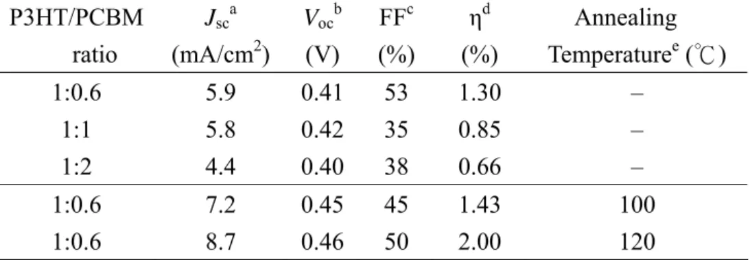
Figure 2-1. Cartoon representation of the well-ordered nanorod structures…………26 Figure 2-2. (a) SEM image of the P3HT/PCBM (1:1, w/w) nanorod array; the inset
displays the ordered Al membrane (scale bar: 100 nm). (b) Top view TEM image of the P3HT/PCBM (1:4, w/w) nanorod structure (scale bar: 50 nm)……….26
Figure 2-3. UV spectrums of P3HT/PCBM(1:1, w/w) as-cast film (circle) and
nanorods structures (square)………27
Figure 2-4. C-AFM (a) topographic vertical distance: 70 nm (b) current images of a
thin film of P3HT/PCBM nanorods and (c) The variation in current between the labeled core (PCBM rich region) and shell (P3HT rich region) regions was 14.3 pA.
……….28 Figure 2-5. J–V characteristics of P3HT/PCBM nanorod array devices prepared after
annealing at various temperatures, measured under AM 1.5G illumination at an intensity of 100 mW/cm2……….29
Chapter 3: Inverted Heterojunction Solar Cells Incorporating Fullerene / Polythiophene Composite Core/Shell Nanorod Arrays
Figure 3-1. (a) Schematic representations of the inverted structure and the
PCBM/P3HT core/shell structure of the inverted solar cell device. (b) Energy level
diagram of the inverted solar cell device. And SEM images of PCBM/P3HT (1:1, w/w) nanorod arrays featuring nanorods having diameters and covered densities (D) on the substrate of (c) 70 nm and 54%, (d) 80 nm and 64%, respectively…………..46
Figure 3-2. (a). Reflectance spectra of PCBM/P3HT nanorod array BHJ solar cell
diameter) /MoO3 (20 nm)/Ag (80 nm); sample only with electrodes: a device fabricated without the active layer. Inset: Schematic representation of the incident light path in a completed device and sample only with electrode. (b) Absorption efficiency (ηA,a) of the devices. (c) EQE spectra of the nanorod array inverted devices and the conventional structure inverted devices .(d) Internal quantum efficiency (ηIQE) spectra of PCBM/P3HT BHJ solar cells (conventional structure; nanorod array with diameter: 80 nm; length: 200 nm)………...49
Figure 3-3. (a) the EQEs of 120nm length nanorods with diameter of 65, 70 or 80nm.
(b) the EQEs of 80nm diameter nanorods with length of 120, 150 or 300nm. (c) the IQEs of 120nm length nanorods with diameter of 65, 70 or 80nm. (d) the IQEs of 80nm diameter nanorods with length of 120, 150 or 300nm………...52
Figure 3-4. (a) J–V characteristics of PCBM/P3HT nanorod array devices
incorporating 120-nm-length nanorods with diameter of 65, 70 and 80nm. (b) J–V characteristics of PCBM/P3HT nanorod array devices incorporating 80-nm–diameter nanorods having lengths of 120, 150, and 300 nm. Devices were measured under AM 1.5G illumination at an intensity of 100 mW cm–2. The thickness of active layer for conventional structure is 120nm………..54
Figure 3-5. Conducting atomic force microscopy (C-AFM) dark J–V curves for
hole-dominated carrier samples incorporating PCBM/P3HT (0.8:1, w/w) in
conventional structure and nanorod array structures. Inset: C-AFM current images of
PCBM /P3HT nanorods………..55 Figure 3-6. J–V characteristics of annealed PCBM/P3HT nanorod array devices
incorporating 80-nm–diameter nanorods having lengths of 120, 150, and 200 nm. Devices were annealed at 120 °C for 10 min and then measured under AM 1.5G illumination at an intensity of 100 mW cm–2………...56
Chapter 4: Nanostructured Nanorod Arrays Presenting TiO2
Nanorods/Poly(3-hexylthiophene) for Solar Cells Application
Figure 4-1. Schematic representations of the TiO2/P3HT nanorod core/shell structure of the inverted solar cell device………72
Figure 4-2. (a) High-resolution TEM (HRTEM) image of TiO2 nanorods. The scale bar is 20nm. (b) X-ray diffraction pattern of TiO2 nanorods………73
Figure 4-3. The TEM images of cross-section and top view of pure P3HT nanorod
array and TiO2 nanorod/P3HT nanorod array with different weight ratio. (a), (b) for pure P3HT, (c), (d) for TiO2 nanorod/P3HT: w/w=1/1. The scale bar is 100nm…….74
Figure 4-4. (a) Normalized optical absorption spectra of the nanorod arrays with
different weight ratio of P3HT/TiO2 and pure P3HT. (b) PL spectra of nanorod arrays, recorded at an excitation wavelength of 500 nm. The size of the nanorod is 110nm long with 80nm diameter………75
Figure 4-5. C-AFM image (Image size: 0.5 μm × 0.5 μm) of TiO2 nanorod/P3HT array (a) topographic image. (vertical distance: 100 nm) and (b) current images of a thin film of TiO2 nanorod/P3HT array; Z-range: 20 pA………..76
Figure 4-6. Conducting atomic force microscopy (C-AFM) dark J–V curves for
hole-dominated carrier samples incorporating TiO2 nanorod/P3HT arrays………….77
Figure 4-7. J–V characteristics of TiO2 nanorod/P3HT array devices. Devices were measured under AM 1.5G illumination at an intensity of 100 mW cm–2……….78
Chapter 5: Synthesis and Characterization of Donor–Acceptor
Poly(3-hexylthiophene) Copolymers Presenting 1,3,4-Oxadiazole Units and Their Application to Photovoltaic Cells
Figure 1. Normalized optical absorption spectra of the self-made P3HT, the
copolymers P05-P20 and comonomer (compound 3) in (a)THF solution (9.6×10⁻⁵ M) and (b) self-made P3HT and the copolymers P05-P20 as thin films (the thickness of film is 90nm on quartz.)……….101
Figure 2. PL spectra of films of the self-made P3HT and the copolymers P05, P15,
and P20, recorded at an excitation wavelength of 450 nm. The thickness of film is 90nm on ITO substrate………...………102
Figure 3. Cyclic voltammograms of films of the self-made P3HT and the copolymers P05, P15, and P20, recorded at a scan rate of 50 mV/s……….103 Figure 4. Current density–voltage characteristics of illuminated (AM 1.5G, 100 mW
cm–2) polymer photovoltaic cells incorporating PCBM blends of the self-made P3HT and the copolymers P05, P15 and P20………..104
Figure 5. (a) EQEs of solar cells incorporating copolymer P15/PCBM and the
self-made P3HT/PCBM blends. (b) Absorption spectra of the copolymer P15/PCBM and the self-made P3HT/PCBM at blend ratios of 1:1………...105
Figure 6. Topographic AFM images of films of PCBM blends (1:1, w/w) with (a) the
self-made P3HT and (b–d) the copolymers (b) P05, (c) P15, and (d) P20. Image size: 2.5 μm × 2.5 μm……….106
Scheme & Table Lists
Chapter 2: Ordered Polythiophene/Fullerene Composite Core–Shell Nanorod Arrays for Solar Cell Applications
Table 2-1. Electronic parameters of vertical p–n junction structure devices prepared
from various P3HT/PCBM weight ratios and annealed at various temperatures…….25
Chapter 3: Inverted Heterojunction Solar Cells Incorporating Fullerene / Polythiophene Composite Core/Shell Nanorod Arrays
Table 3-1. External quantum efficiencies (EQEs) and internal quantum efficiencies
(IQEs) at 520nm from nanorods of various sizes………....….44
Table 3-2. Electronic parameters of vertical p–n junction devices prepared from
nanorods of various sizes……….44
Table 3-3. Electronic parameters of annealed vertical p–n junction devices prepared
from nanorods of various sizes……….45
Chapter 4: Nanostructured Nanorod Arrays Presenting TiO2 Nanorods/Poly(3-hexylthiophene) for Solar Cells Application
Table 4-1. Electronic parameters of one dimensional structure array devices prepared
from various P3HT/TiO2 nanorod weight ratios………..71
Chapter 5: Synthesis and Characterization of Donor–Acceptor
Poly(3-hexylthiophene) Copolymers Presenting 1,3,4-Oxadiazole Units and Their Application to Photovoltaic Cells
Table 5-1. Polymerization Data and Thermal Properties of the Copolymers………..98 Table 5-2. Optical and Redox Properties of the Copolymers………..98
Table 5-3. Photovoltaic Properties of Polymer Photovoltaic Cells Incorporating
Blends (1:1, w/w) of P3HT/PCBM and P05–P20/PCBM………...99
Scheme 5-1. Synthetic Routes Toward M1 and M2………..100 Scheme 5-2. Synthetic Route Toward the Copolymers……….100
Appendix
Chapter 2: Ordered Polythiophene/Fullerene Composite Core–Shell Nanorod Arrays for Solar Cell Applications
FigureA.2-1. Grazing-incidence XRD diffraction diagrams of P3HT/PCBM(1:1, w/w)
as-cast films, identically annealed at 120℃ for 10 minutes and P3HT/PCBM
nanorods structure. The increase at 2Ө~50(interchain distance of interdigitated alkyl chain in P3HT) and 2Ө~220 (interchain distance of face-to-face packing of the
thiophene ring)are observed. That means crystallinity is improved………30
Figure A.2-2. Atomic force microscopy (AFM) topographic images for of a thin film
P3HT/PCBM nanorods structure. The image size is 1.48µm×1.48µm, and the vertical scale is 70 nm………...31
Figure A.2-3. Scanning electron microscopy (SEM) images of the P3HT/PCBM
nanorod nanostructures. The length of rod is 110nm………...32
Chapter 3: Inverted Heterojunction Solar Cells Incorporating Fullerene / Polythiophene Composite Core/Shell Nanorod Arrays
Figure A3-1. Large-area SEM image of the PCBM/P3HT (1:1, w/w) nanorod array;
inset: magnified image (scale bar: 100 nm)……….57
Figure A3-2. SEM images of PCBM/P3HT (1:1, w/w) nanorod arrays having lengths
of (a) 200 and (b) 300 nm. Inset to (b): Cartoon representation of the structure in the cross-sectional image………...58
Figure A3-3. (a) Cross-sectional SEM image of ITO glass/TiOx; the thickness of the TiOx layer was 45 nm. (b) AFM image of glass/TiOx surface; the RMS roughness of this film was 1.2 nm……….58
Figure A3-4. (a) and (b) reflectance spectra of PCBM/P3HT nanorod array with
different diameters (65nm to 80nm) and length (120nm to 300nm) respectively, solar cell devices. (c) and (d) absorption efficiency (ηA,a) of the devices with different diameters and lengths, respectively………..59
Chapter 5: Synthesis and Characterization of Donor–Acceptor
Poly(3-hexylthiophene) Copolymers Presenting 1,3,4-Oxadiazole Units and Their Figure A5-1. Display the 1H NMR spectra of self-made P3HT and copolymer
P05-P20. (a) self-made P3HT, (b) P05, (c) P15, (d) P20………...110 Figure A5-2. shows the dihedral angel between the plane of thiophene and the plane
of 1,3,4-oxadiazole moiety simulated from the ChemBio3D Ultra software. The dihedral angel between the polymeric main chain and the 1,3,4-oxadiazole moiety is 32.11˚………..111
Figure A5-3. The Photoluminescence of the comonomer (compound 3) in THF
solution (9.6×10⁻⁵ M) recorded at an excitation wavelength of 310 nm………112
Figure A5-4. Synchrotron Grazing-incidence XRD diffraction diagrams of self-made
P3HT and copolymer P05-P20 as-cast films (100nm on ITO substrate), identically annealed at 150◦C for 10 min. The decrease at 2θ~5◦ (interchain distance of
interdigitated alkyl chain in Polythiophene backbone) is observed obviously for P20. That means ordering of polymer chain is decreased………..113
Chapter 1: Introduction
1-1 Introduction of Polymer Solar cell
Conjugated polymers possessing extended delocalized π electrons are being investigated intensively for their potential uses in such organic optoelectronic devices as light emitting diodes (LEDs), thin film transistors, and photovoltaic cells
incorporating bulk heterojunctions (BHJ).1–8 In the last fifteen years, a significant progress has been made on the improvement of the power-conversion efficiency (PCE) of polymer BHJ solar cells, and the achieved efficiencies have evolved from less than 1% in the poly(phenylene vinylene) (PPV) system in 1995, to 4–5% in the
poly(3-hexylthiphene) (P3HT) system 9–12, as reported in 2005. The PCE value was further improved to 7%13 in recent year. The improvement of PCE resulted from the development of novel conjugated polymer with low band gap, high open-circuit voltage and the well-controllable nanoscale morphology of composite film. Here a brief introduction and overview is given of the field of polymer solar cell.
This dissertation is organized as follow. In the first part, we will give the work principles, critical parameters, the materials, wetting transition of polymers and the nanostructured polymer solar cell. In the second part, we will focus on our recently studies of fabricate and characterize the core-shell nanorod arrays of
efficiency, hole mobility, and the performance of conjugated polymer/fullerene BHJ solar cells are investigated. In the third part, we will discuss nanostructured arrays of conjugated polymer/inorganic nanocrystals for solar cell application. In the fourth part, a new class of conjugated polymer was synthesized and characterized for solar cell application. Finally, we will finish with some conclusions.
1-2 The Principle of Polymer Solar Cell
1-2-1 Mechanisms leading to the charge generation and collection in organics
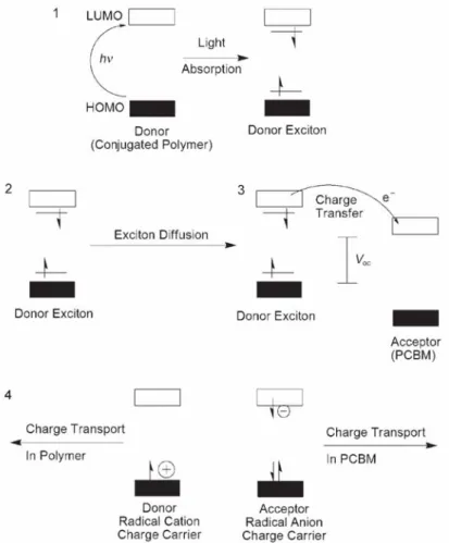
Efforts to optimize the performance of organic solar cells should find their basis in the fundamental mechanism of operation. Figure 1-1 illustrates the mechanism by which light energy is converted into electrical energy in the devices. The energy conversion process has four fundamental steps in the commonly accepted
mechanism:[14] (1) Absorption of light and generation of excitons, (2) diffusion of the excitons, (3) dissociation of the excitons with generation of charge, and (4) charge transport and charge collection. Figure 1-1 shows a schematic representation of a typical BHJ solar cell, illustrating the components involved in the mechanistic steps as well as a current–voltage curve defining the primary quantities used to validate the performance of a solar cell.
generation of free charges are shown in Figure 1-2.[15, 16] The processes can also occur in an analogous fashion in the case of an excited acceptor, and the details of these mechanistic steps have been described extensively in the literature.[17] The key point is that electron transfer is not as simple as depicted in Figure 1-1. The process must be energetically favorable to form the geminate pair in step 3 of Figure 1-2 and an
energetic driving force must exist to separate this Coulombically bound electron–hole pair. The open circuit voltage (Voc) is also governed by the energetic relationship between the donor and the acceptor (Figure 1-3) rather than the work functions of the cathode and anode, as would be expected from a simplistic view of these diode devices. Specifically, the energy difference between the HOMO of the donor and the LUMO of the acceptor is found to most closely correlate with the Voc value.[18, 19] Figure 1-3 shows a schematic drawing of the energy levels in an organic solar cell. The maximum short-circuit current is determined by the smaller optical band gap of the two materials, and Voc is proportional to the difference between the HOMO level of the donor material and the LUMO level of the acceptor compound. For an efficient charge generation in the donor–acceptor blend, a certain offset of the HOMO and LUMO levels (ΔEHOMO, ΔELUMO) is required,[20] which is believed to be a few
hundred milli-electron Volts. This offset, a minimum energy offset of 0.3 eV between the donor and acceptor, which is often referred to as the exciton binding energy,[21]
determines the ultimate device efficiency of bulk-heterojunction solar cells.[22-23]
Figure 1-1 General mechanism for photo energy conversion in solar cells.
Figure 1-2 Elementary steps in the process of photoinduced charge separation for a donor (D) and an acceptor (A):
(1) Photoexcitation of the donor;
(2) diffusion of the exciton and formation of an encounter pair;
(3) electron transfer within the encounter pair to form a geminate pair; (4) charge separation.
1-2-2 Characterization of a solar cell device
The current-voltage characteristics of a solar cell in the dark and under
illumination are shown in Figure 1-4. In the dark, there is almost no current flowing, until the contacts start to inject at forward bias for voltages larger than the open circuit voltage. The device generates power under light. At maximum power point (MPP), the product of current and voltage is the largest.[24] The photovoltaic power
conversion efficiency (ηe) of a solar cell is determined by the following formula:
where Voc is the open circuit voltage, Isc is the short circuit current, FF is the fill factor, and Pin is the incident light power density. This light intensity is standardized at 1000 W/m2 with a spectral intensity distribution matching that of the sun on the earth’s surface at an incident angle of 48.2°, which is called the AM 1.5 spectrum.[25] Impp and Vmpp are the current and voltage at the maximum power point.
(IPCE) is simply the number of electrons collected under short circuit conditions, divided by the number of incident photons. IPCE is calculated using the following formula:
where λ [nm] is the incident photon wavelength, Isc [µA/cm2] is the photocurrent of the device, and Pin [W/m2] is the incident power.
Figure 1-4: The Characterization of a solar cell device. Current-voltage (I-V) curves of an organic solar cell (Dark, - - -; illuminated, -). The characteristic intersections with the abscissa and ordinate are the open circuit voltage (Voc) and the short circuit current (Isc), respectively. The largest power output (Pmax) is determined by the point where the product of voltage and current is maximized. Division of Pmax by the product of Isc and Voc yields the fill factor FF.
1-3 Literature Review of Polymer Solar Cell
1-3-1 Materials: Polymers and Inorganic Nanocrystals
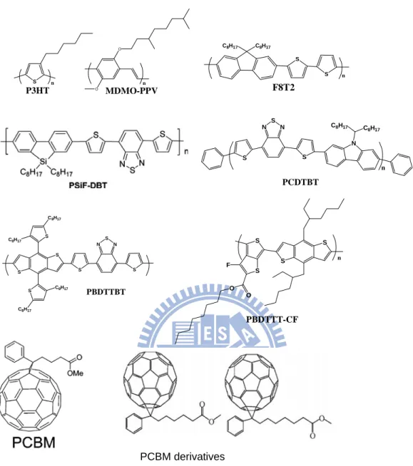
Generally, the organic materials having a delocalized π electron system can absorb sunlight, create photogenerated charge carriers, and transport these charge carriers for solar cell application. The conjugated polymers are named as the electron donor polymer in a BHJ solar cell device. Figure 1-5 shows the conjugated polymers which are widely applied to polymer solar cell devices. At present, the polymers poly(3-hexylthiophene)(P3HT), poly[2-methoxy- 5-(3,7-dimethyloctyloxy)] -1,4-phenylenevinylene) (MDMOPPV), and poly[2,7-(9,9-dihexylfluorene)-alt- bithiophene] (F8T2) have been applied to polymer solar cell. However, the narrow absorption spectrum of polymers in 300–650 nm is one of the main hindrances to the further improvement of the efficiencies of conjugated polymer-based solar cell devices. To overcome this problem, some low-band-gap polymer materials as donors have been synthesized successfully and applied to photovoltaic devices.
Recently, the polymers with high open-circuit voltages and consequently high PCEs (above 5 %) have been reported and further investigated for three kinds of polymers, poly[(2,7-silafluorene)-alt-(4,7-di-2-thienyl-2,1,3-benzothiadiazole)] (PSiFDBT), poly[N-9’’-heptadecanyl-2,7-carbazole-alt-5,5-(4’,7’-di-2-thienyl- benzothiadiazole) (PCDTBT), and poly{4,8-bis(2,5-dioctyl-2-thienyl)-benzo
[1,2-b:4,5-b’]dithiophene -alt-[4,7-bis(2-thienyl)-2,1,3-benzothiadiazole)-5,5’-diyl]} (PBDTTBT).[26-29] Furthermore, the performance of PBDTTT-CF, the derivatives of
PBDTTBT, shows PCE value of 7 %.[13, 30,31] There are number of excellent in-depth
reviews covering materials selection for polymer solar cells.[32-37]
The electron acceptor like Fullerenes derivatives [6,6]-phenyl-C61-butyric acid methyl ester (PCBM), and PC70BM is most commonly used when blended with a light absorbing and hole-conducting conjugated polymer to afford the
bulk-heterojunction active layer in a photovoltaic device (shown in Figure 1-5). The [6,6]-phenyl-C61-butyric acid methyl ester (PCBM)-like fullerene derivatives with the different side chain in PCBM are designed and synthesized to investigate the relationship between photovoltaic properties and the molecular structure of fullerene derivative acceptors.[38,39]
Various hybrid polymer solar cells such as polymer:inorganic-nanoparticle BHJs have been reported, using CdSe nanodots, nanorods,[40] and tetrapods,[41,42] and nanoparticles of TiO2,[43] ZnO,[44,45] PbS,[46,47] PbSe,[48,49] and CuInSe2.[50] In a related approach, nanostructured TiO2 has been filled with conjugated polymers,[51–56] but up to now random mixtures of conjugated polymers and inorganic nanoparticles have given the better efficiencies.
Figure 1-5 The example of organic semiconductors used in polymer solar cells. The structure of P3HT, MDMO-PPV, F8T2, PSiF-DBT, PCDTBT, PBDTTBT,
PBDTTT-CF, PCBM, and PCBM derivatives. S n O O n P3HT MDMO-PPV C8H17 C8H17 S S n F8T2 N S N N C8H17 C8H17 S S n PCDTBT S S S S C8H17 C8H17 C8H17 C8H17 S S N S N PBDTTBT S S F O O S S n PBDTTT-CF PCBM derivatives
1-3-2 the wetting transition in nanopores of conjugated polymer
The wetting of a solid substrate with a liquid has attracted substantial interest because of its various technical applications, including coatings, lubrication, adhesion, painting, and nanoimprinting. Different wetting regimes can be classified according to the spreading coefficient S, which is definedby[59-61]
where, γSG, γSL, and γ represent the solid-gas, solid-liquid, and liquid-gas interfacial tensions, respectively. S measures the interfacial energy difference between the bare substrate and the substrate covered with a film of liquid. If S ≥ 0, complete wetting will occur and a liquid droplet will spread spontaneously on the solid substrate until a complete coverage of the substrate with a thin liquid film is achieved. If S < 0, a liquid drop deposited on the solid substrate will spread partially. Wetting, in the case of a negative spreading coefficient, is called partial wetting.
The wetting of porous templates with polymer melts and solutions or
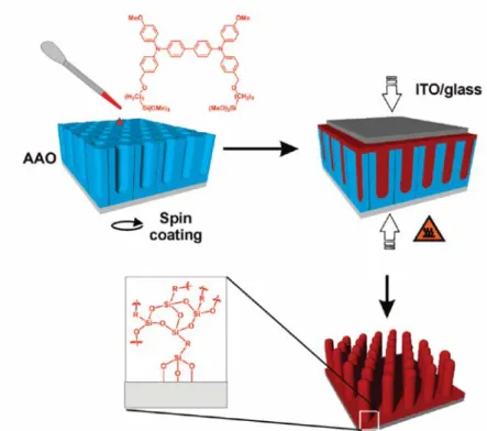
polymer-containing mixtures is a simple and versatile method for the preparation of tube or rod structures with diameters ranging from a few tens of nanometers to micrometers. Template wetting also makes it possible to modify the nanotubes in a variety of ways, for example through the controlled generation of pores or the
functionalized nanorods– template hybrid systems and free-standing nanorods. For example, the Poly(9,9-dioctylfluorene) (PFO) polymer nanowires was fabricated by melt-assisted wetting of porous alumina templates.[57] The single-nanowire imaging, spectroscopy, and nano-optical behavior were investigated for waveguides application. The template-based preparation of free-standing semiconducting polymeric nanorod arrays on conductive substrates is currently reported. The topography and local conductivity variations on fragile free-standing nanopillar arrays were investigated. The local current-voltage characteristics suggest a space-charge limited conduction in thesemiconducting nanopillars. These nanorod arrays are highly interesting for the fabrication of multilayered device architectures to be used in organic photovoltaics. [58]
The pure P3HT nanorods oriented perpendicularly to indium tin oxide (ITO) glass are fabricated using an anodic aluminum oxide template.Furthermore, the donor/acceptor contact area of polymer solar cells could be increasing for using P3HT nanorods as donor and C60 as acceptor. In a photovoltaic device employing this structure,
remarkable photoluminescence quenching (88%) and a seven-fold efficiency increase (relative to a device with a planar bilayer) are achieved. [59]
Figure 1-6 Schematic diagram of the template-assisted fabrication of cross-linked free-standing nanorod arrays. [58]
1-3-3 Inverted solar cell
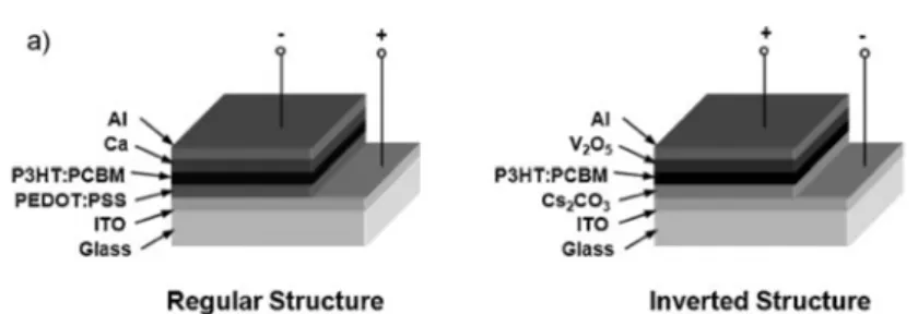
In most regular solar cell devices, the hole-collecting electrode consists of both an acidic PEDOT: PSS layer on high-work-function transparent conducting oxide, and a low work function metal as electron-collecting electrode. In such a device, the oxidation of air-sensitive low-work-function metal cathode such as Al and the degradation of indium tin oxide (ITO/poly (3, 4-ethylene dioxythiophene): (polystyrene sulfonic acid) (PEDOT:PSS) interface represents an instability that demands encapsulation techniques to prevent exposure to air [62,63]. The TiOx and ZnO (Zinc Oxide) [64-67] as electron collecting electrode and the V2O5 (Vanadium (V) oxide) and MoO3[68-70] (Molybdenum (VI) oxide) as hole transport layer are used to replace Al and PEDOT: PSS for the fabrication of polymer heterojunction solar cell device with an inverted geometry. Furthermore, this inverted structure has been shown that high-workfunction metals such as Au and Ag[71,72] can be deposited onto
polymer/metal oxide layers via thermal evaporation to prevent the oxidation of electrode.
Figure 1-7 Schematic depiction of the regular structure and inverted structure of the polymer solar cell devices.
1-4 Motivation
The morphology of the photoactive layer P3HT/PCBM without post treatment does not have severe suitable phase separation. However, the ordering of donor material (P3HT) and acceptor (PCBM,or inorganic crystals) domain size of phase separation which contribute to the charge transfer and percolation do not develop adequately. In particular, because the ordering and phase separation occur
simultaneously with post treatment, it is difficult to control the morphology to achieve the optimum state. Therefore, the fabrication of an ordered bulk heterojunction that can help enhance charge transport and overcome exciton recombination is a
promising way to obtain high performance solar cell devices. [73–75] Such structures
offer solar cell performance advantages compared with the planar bilayer, such as efficient charge extraction by the increase of donor–acceptor interfacial area, the decrease of exciton recombination loss, carrier transfer time and reverse electron transfer, and retention of the electron and hole pathways.[76,77] Therefore, we try to
fabricate ordered conjugated polymer/ nanoparticle composite nanorod arrays which contribute efficient transport of electrons and holes along the phase-separated regions in the nanorod array structure, respectively.
For the development of novel materials, the conjugated polymers containing electron donor–acceptor pairs in the polymeric main chain and/or side chains has
become quite attractive recently78–85 because such system exhibit tunable electronic properties and enlarged spectral absorption ranges. Alternatively, the introduction of a side-chain electron-acceptor unit—usually a conjugated species that absorbs a wavelength different from that of the conjugated polymer—can increase the breadth of the wavelengths of light absorbed. Furthermore, the photogenerated excitons can be dissociated into electrons and holes more efficiently in these types of conjugated polymer because of the internal field produced by the inherent dipole moment resulting from the donor–acceptor molecular structure, with subsequent charge transfer to nearby n-type nanoparticles (e.g., PCBM). Therefore, we developed a new class of donor–acceptor thiophene-type copolymer presenting electron-withdrawing 1,3,4-oxadiazole moieties as side chains for application in photovoltaic cells.
Chapter 2:
Ordered Polythiophene/Fullerene Composite Core–Shell
Nanorod Arrays for Solar Cell Applications
2-1 Introduction Materials
The development of conjugated polymers for use in organic optoelectronic devices has advanced dramatically in recent years. In particular, polymer heterojunction solar cell devices are receiving considerable attention.[1, 5, 86–90] Typically, the active layer of a polymer heterojunction solar cell is prepared from a thin film of an electron-donating conjugated polymer and an electron-accepting species. The power conversion efficiency (PCE) of polymer hetrojunction solar cells has improved dramatically over the last few years; those containing blends of
regioregular poly(3-hexylthiophene) (P3HT) and [6,6]-phenyl-C61-butyric acid methyl ester (PCBM), have recently reached PCEs of ca. 4–5% under standard solar conditions (AM 1.5G, 100 mW/cm2).[91–93]
There is generally no preferred direction for the internal fields of separated charges for a polymer heterojunction solar cell device; that is, the electrons and holes created within the volume have no net resulting direction in which they should move. [33] Furthermore, because the separated holes and electrons require percolated
pathways for transport to their contacts,device structures containing a two-phase donor/acceptor film must exhibit features interspaced with an average length of ca.
the losses that arise from recombination of charges moving in the wrong direction. The wetting of porous alumina membrane (AAO) templates with polymer melts, solutions, or polymer-containing mixtures is a simple and versatile method for the fabrication of one-dimensional structures having diameters ranging from a few tens of nanometers to several micrometers. This approach is a promising one for preparing functionalized nanorod–template hybrid systems and free-standing nanotubes and nanorods.[61, 94–96] Additionally, the hole mobility of a pure P3HT nanowire in a straight AAO pore is enhanced by as much as a factor of 20 compared with that in a neat film[97] because the polymer chains are partially aligned in the charge-transport direction after infiltrating the vertically straight nanopores of the anodic alumina. Therefore, in this present study, we used the wetting of ordered AAO templates to fabricate (figure 2-1) P3HT/PCBM core–shell nanorods for use in solar cell devices. We expect that such ordered nanorod structures will provide more-efficient polymer solar cells.
2-2 Experimental
We prepared P3HT/PCBM films having a thickness of 120 nm through solution casting onto ITO glass slides and then placed an alumina membrane (AAO) on top of the P3HT/PCBM film. This P3HT/PCBM film/alumina membrane was sandwiched
between two glass slides and then placed in an oven and annealed under vacuum. After 6 h, the assembled system was cooled to room temperature. Dissolving the alumina membranes in 10 wt% NaOH solution released the P3HT/PCBM core–shell nanorod structures, which were dried under vacuum for 12 h prior to characterization. Scanning electron microscopy (SEM) images of the resultant P3HT/PCBM
nanostructures were investigated using a JEOL 6500 model scanning electron
microscope at an accelerating voltage of 15 kV. The samples were coated with a thin layer of platinum (thickness: ca. 3 nm) prior to SEM imaging. Transmission electron microscopy (TEM) images were obtained using a Hitachi H-600 transmission electron microscope. The sample for the TEM analysis was prepared by removing the nanorod array thin film from the ITO substrate with 1% HF, and then collecting the thin film with a TEM Grid coated with carbon. We performed conductance atomic force microscopy (C-AFM) experiments using platinum-coated silicon cantilevers [NanoSensors Inc. (PPP-ContPt, spring constant k = 0.2 N/m)] and a Digital
Nanoscope Ⅳ operated under ambient conditions. The current density–voltage (J–V) characteristics of the polymers were measured using devices having the structure ITO/PEDOT:PSS/P3HT:PCBM/Al. The ITO-coated glass substrate was pre-cleaned and treated with oxygen plasma prior to use. The P3HT/PCBM layer was spin-coated from a chlorobenzene solution. Using a base pressure below 1 × 10⁻⁶ torr, a layer of
Al (100 nm) was vacuum-deposited as the cathode. Testing of the devices was performed under simulated AM 1.5G irradiation (100 mW/cm2) using a xenon lamp-based Newport 66902 150W solar simulator equipped with an AM1.5 filter as the white light source; the optical power at the sample was 100 mW/cm2, detected using an OPHIR thermopile 71964. The current density–voltage (J–V) characteristics were measured using a Keithley 236 source-measure unit.
2-3 Results and Discussions
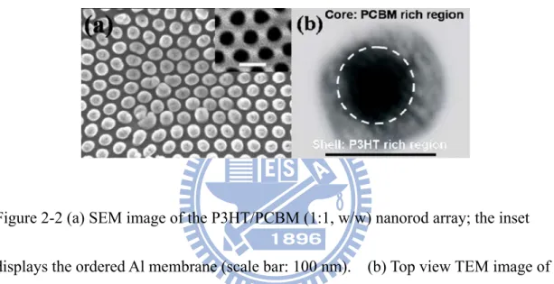
Figure 2-2a displays an SEM image of the P3HT/PCBM (1:1, w/w) nanorod array structure. The average diameter of the nanorods was ca. 65 nm, equal to the diameter of the nanopores (65 nm) in the ordered AAO membrane (inset to Figure 2-2a). Figure 2-2b provides a TEM top-view image of the P3HT/PCBM (1:4, w/w) nanorods, revealing their core–shell-like structures; the dark central region of the nanorods represents the PCBM-rich region, which has a higher electron density than that of the P3HT-rich region.
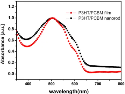
Intensity normalized absorption spectrum of P3HT/PCBM (1:1, w/w) thin film and nanorods are shown in figure 2-3. The maximum absorption (λmax) took place at ca. 504 nm for the P3HT/PCBM thin film, resulting from π–π* transitions. In comparison, the absorption peak of P3HT/PCBM nanorod array shifted slightly
towards a lomger wavelength at 508 nm displayed. The Full-width-at-half -maximum (FWHM) increase to 231nm for P3HT/PCBM nanorod array from 173nm for
P3HT/PCBM thin film, an increase of 58nm.
Figure 2-4 displays C-AFM images of the P3HT/PCBM (1:1, w/w) nanorods embedded onto the ITO glass substrate. In the topographic image (Figure 4a), the light regions having a height of ca. 70 nm represent the P3HT/PCBM nanorods. In the current image (Figure 4b), measured at a sample bias of –1 V, the currents of the
P3HT/PCBM nanorods (light regions) were ca. 30 pA, whereas those of the spaces
between the rods (dark regions) were at the level of the noise (ca. 0.5 pA); this image also reveals the contrast between the current images of the core and shell regions. The current resulted mainly from hole transport because Pt and ITO have high work functions of ca. 5.7 and 4.8 eV, respectively. Because the Pt-coated tip was biased, the influence of the surface electrical properties of ITO played only a minor role [98]. We observed a variation in current of 14.3 pA between the charge transport of the core and shell regions of the nanorods, despite have some inhomogeneities in their compositions. This phenomenon resulted primarily from the composition difference between the core and shell region, where the dark central region of the nanorods represent the PCBM-rich region and the light region of the nanorods represent the P3HT-rich region. The nanorods of the P3HT/PCBM blend possessed core–shell
structures, with the P3HT-rich regions of the shell evident in the C-AFM current image. Therefore, we expected most of the electron/hole pairs to separate at the p–n interface, such that the electron and hole transport would occur through the
PCBM-rich region (n-type) and P3HT-rich region (p-type) individually and
efficiently in this core–shell structure.
The phase separation of P3HT/PCBM blends in the wetting of porous AAO
membrane is determined by the flow induced shear stress, which is the largest along the AAO pore wall and is the lowest in the center of AAO pore. Since the viscosity of PCBM is much larger than that of P3HT at 120 , the largest stress along the AAO ℃ pore wall will induce lower viscosity part of the blend, i.e. P3HT rich region to flow along. Whereas, the minimum stress in the center of AAO pore will have higher viscosity part of the blend, PCBM rich region, to flow along. Consequently, this phase separation of the P3HT/PCBM blend during flow results in the core-shell structured nanorods after quenching to room temperature.
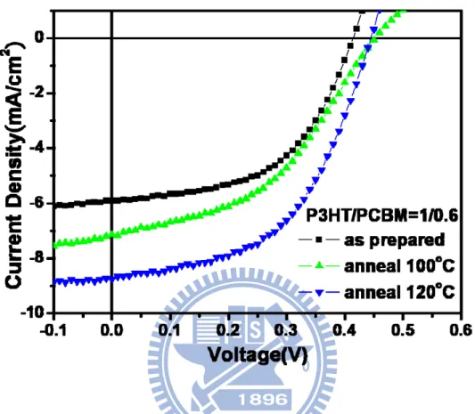
Figure 2-5 displays the J–V characteristics of solar cell devices incorporating ordered nanorods of various compositions. The performance increased upon decreasing the
PCBM content(Table 2-1). For the device containing P3HT and PCBM at a 1:2 ratio
(w/w), the values of the short circuit current density (Jsc), the fill factor (FF), and the PCE were 4.4 mA/cm2, 38%, and 0.66%, respectively; these values increased to 5.9
mA/cm2, 53%, and 1.30%, respectively, for the 1:0.6 (w/w) P3HT/PCBM device. This improvement in efficiency might be caused by more efficient charge transport in the device structure, due to the high difference in their composition of core and shell. To improve the performance of our solar cell devices, we subjected them to annealing at various temperatures. For the device incorporatingP3HT/PCBM at a 1:0.6 ratio
(w/w), the values of PCE and Jsc improved to 2.0% (from 1.3%) and 8.7 mA/cm2 (from 5.9 mA/cm2), respectively, after thermal annealing at 120 °C for 10 min. This improved performance after annealing quite possible resulted from increases in the degree of crystallization, [10] the transport properties, [99] and the light absorption [100] of the P3HT-rich region and also from the improved contact at the electrode for the transfer of electrons. The area covered by the nanorods on the substrate determines the amount of incident light absorbed. In our devices, this area was ca. 43% (defined by the AAO membrane) of the total substrate surface. Hence, increasing the packing density of the nanorods so that they occupy a greater percentage of the surface area might improve the devices’ performance further so that they would have potential for use in solar cell applications.
2-4 Conclusions
to fabricate vertical nanorod arrays of P3HT and PCBM having core–shell
nanostructures for application in polymer solar cells. C-AFM current images revealed the difference of charge transport behavior of the core and shell moieties.
TABLE 2-1. Electronic parameters of vertical p–n junction structure devices prepared from various P3HT/PCBM weight ratios and annealed at various temperatures. P3HT/PCBM ratio Jsca (mA/cm2) Vocb (V) FFc (%) ηd (%) Annealing Temperaturee ( )℃ 1:0.6 5.9 0.41 53 1.30 – 1:1 5.8 0.42 35 0.85 – 1:2 4.4 0.40 38 0.66 – 1:0.6 7.2 0.45 45 1.43 100 1:0.6 8.7 0.46 50 2.00 120
aShort-circuit current density. bOpen circuit voltage.
cFill factor.
dPower conversion efficiency. eAnnealing time: 10 min.
Figure
Figure 2-1 Cartoon representation of the well-ordered nanorod structures.
Figure 2-2 (a) SEM image of the P3HT/PCBM (1:1, w/w) nanorod array; the inset displays the ordered Al membrane (scale bar: 100 nm). (b) Top view TEM image of the P3HT/PCBM (1:4, w/w) nanorod structure (scale bar: 50 nm).
Figure 2-3 UV spectrums of P3HT/PCBM(1:1, w/w) as-cast film (circle) and nanorods structures (square).
Figure 2-4 C-AFM (a) topographic vertical distance: 70 nm (b) current images of a thin film of P3HT/PCBM nanorods and (c) The variation in current between the labeled core (PCBM rich region) and shell (P3HT rich region) regions was 14.3 pA
Figure 2-5 J–V characteristics of P3HT/PCBM nanorod array devices prepared after annealing at various temperatures, measured under AM 1.5G illumination at an intensity of 100 mW/cm2.
Appendices
FigureA.2-1 Grazing-incidence XRD diffraction diagrams of P3HT/PCBM(1:1, w/w) as-cast films, identically annealed at 120℃ for 10 minutes and P3HT/PCBM
nanorods structure. The increase at 2Ө~50(interchain distance of interdigitated alkyl chain in P3HT) and 2Ө~220 (interchain distance of face-to-face packing of the thiophene ring)are observed. That means crystallinity is improved.
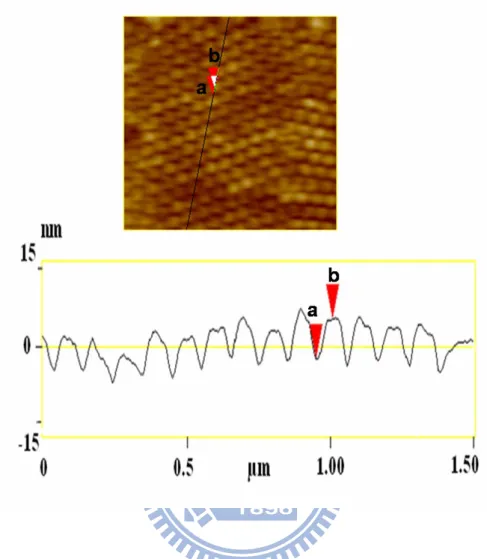
Figure A.2-2 Atomic force microscopy (AFM) topographic images for of a thin film P3HT/PCBM nanorods structure. The image size is 1.48µm×1.48µm, and the vertical scale is 70 nm.
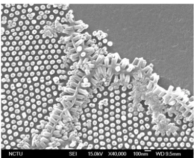
Figure A.2-3 Scanning electron microscopy (SEM) images of the P3HT/PCBM nanorod nanostructures. The length of rod is 110nm.
Chapter 3:
Inverted Heterojunction Solar Cells Incorporating Fullerene /
Polythiophene Composite Core/Shell Nanorod Arrays
3-1 Introduction Materials
The development of conjugated polymers for use in organic optoelectronic devices is an active field of research. In particular, polymer heterojunction solar cells have attracted much attention because of their potential application in large-area, flexible, low-coast devices. [1–7, 86] The power conversion efficiencies (PCEs) of bulk
heterojunction (BHJ) solar cells have improved dramatically over the last few years. For example, the PCEs of BHJ solar cells incorporating regioregular
poly(3-hexylthiophene) (P3HT) as the donor and [6,6]-phenyl-C61-butyric acid methyl ester (PCBM) as the acceptor have recently reached values of ca. 4–5% under standard solar conditions (AM 1.5G, 100 mW/cm2). [8–12, 92] Nevertheless, the PCEs of these polymer BHJ devices must improve further if they are to be employed
practically, necessitating the development of unconventional structures. Alternating donor and acceptor phases possessing vertically aligned geometries, such as
alternating nanorods, appear to be ideal structures for independent carrier transport.[101,102] These structures are, however, difficult to obtain because of the complexity of the fabrication tools available. For the production of ordered polymeric nanorod arrays, template-based approaches are probably most suitable.
Inverted BHJ devices incorporating metal oxides[64-69, 103] such as TiO
x and MoO3 as electrodes and high-work-function anodes (e.g., Ag and Au) have been developed recently because of avoiding the problems of oxidation,[62,63] which occurs in low-work-function cathodes, and degradation of the indium tin oxide
(ITO)–poly(ethylenedioxythiophene) (PEDOT) interface, which occurs frequently in conventional solar cell structures. In this study, we use core/shell-structured
PCBM/P3HT nanorod arrays as the active layer, which we fabricated using an anodic
aluminum oxide (AAO) membrane, to construct an inverted solar cell. To the best of our knowledge, this is the first report of PCBM/P3HT nanorod arrays being
incorporated into inverted BHJ solar cells. Our approach has several advantageous features (Figure 3-1): (ⅰ) the energy level of the highest occupied molecular orbital (HOMO) of the shell (P3HT-rich region) can match that of the metal oxide electrode deposited for hole transport on the shell; (ⅱ) the energy level of the lowest
unoccupied molecular orbital (LUMO) of the core (PCBM rich region) can also match that of the other metal oxide layer for the transport of electrons; and (ⅲ) the direct transport of holes and electrons along the phase-separated shell and core, respectively, occurs in the nanorods. Hence, we expected that such core/shell nanorod array devices featuring a high covered density of nanorods on the substrate and an inverted device geometry would provide more-efficient devices.
3-2 Experimental Section
Regioregular P3HT (4002-E, Rieke Metals), PCBM (Nano-C, Inc.), and poly(3,4-ethylenedioxythiophene: polystyrenesulfonate) (PEDOT: PSS) (Baytron P VP Al 4083, Inc.) were obtained commercially.
A solution of titanium isopropoxide (Alfa, 99.995%; 10 wt%) in isopropyl alcohol was spin-coated onto pre-cleaned ITO glass substrates under a N2 ambient and then it was converted to 40-nm–thick TiOx via hydrolysis at room temperature in air for 2 h. The substrate was then heated at 450 °C for 30 min to complete the hydrolysis reaction.
PCBM/P3HT films of various thicknesses were prepared through solution
casting onto ITO/TiOx substrates; an AAO membrane was then placed on top of the
PCBM/P3HT films. This PCBM:P3HT film/AAO membrane was sandwiched
between two glass slides and then placed in an oven and annealed at 120 °C under vacuum. After 6 h, the assembled system was cooled to room temperature. Dissolving the alumina membranes in 10 wt% NaOH solution released the PCBM/P3HT
core/shell nanorod structures, which were dried under vacuum for 12 h prior to characterization. SEM images of the resultant PCBM/P3HT nanostructures were recorded using a JEOL 6500 scanning electron microscope operated at an accelerating voltage of 15 kV. The samples were coated with a thin (ca. 3 nm) layer of Pt prior to
SEM imaging.
The current density–voltage (J–V) characteristics of the polymers were measured using devices having the structure ITO/TiOx/ PCBM:P3HT /MoO3/Ag. The
ITO-coated glass substrate was pre-cleaned and treated with oxygen plasma prior to use. The TiOx layer was prepared using the spin-coating process described above. The
PCBM/P3HT layer was spin-coated from a chlorobenzene solution. Using a base
pressure of less than 1 × 10⁻⁶ torr, layers of MoO
3 (20 nm) and Ag (80 nm) were vacuum-deposited to form the anode.
The devices were tested under simulated AM 1.5G irradiation (100 mW cm–2) using a Xe lamp–based Newport 66902 150W solar simulator equipped with an AM1.5 filter as the white light source; the optical power at the sample was 100 mW cm–2, detected using an OPHIR thermopile 71964. The J–V characteristics were measured using a Keithley 236 source-measure unit. The EQEs were measured using a Keithley 236 source-measure unit coupled with an Oriel Cornerstone 130
monochromator. The light intensity at each wavelength was calibrated using an OPHIR 71580 diode.
The Hole-only sample, used to investigate hole transport in the polymer/PCBM layers, were fabricated with the structure of ITO/PEDOT/nano rod array. The J–V curves was measured using a conductive atomic force microscopy (C-AFM)
experiments using platinum-coated silicon cantilevers [NanoSensors Inc. (PPP-ContPt, spring constant k = 0.2 N/m), tip diameter ~20nm] and a Digital Nanoscope Ⅳ
operated under ambient conditions. For J–V measurement of C-AFM, we determined the contact area between tip and sample assuming a 20nm diameter circle. The J–V curves from each sample were averaged from four different regions.
3-3 Results and Discussion
Figures 3-1a and 3-1b provide a schematic representation of the PCBM/P3HT core/shell nanorod arrays in an inverted solar cell structure and an energy level diagram for each material, respectively. In this nanorod-based inverted architecture, we positioned a TiOx layer between the ITO glass and the active layer because it is an appropriate material for the electron-collecting ITO/TiOx bottom electrode. The energy level of the LUMO of TiOx is –4.4 eV, which suggests that electrons (LUMO of PCBM: –4.3 eV) can be injected into the TiOx interlayer, while the holes from the active layer blend levels can be effectively blocked (HOMO of TiOx: –7.5 eV). The thickness of the TiOx thin film was 45 nm; its root-mean-square (RMS) roughness, determined through atomic force microscopic analysis, was 1.2 nm (see Appendix: Figure A3-3). In this study, the configuration of the device, stacked from bottom to top, was ITO/TiOx/ PCBM:P3HT (0.8:1, w/w) nanorod arrays/MoO3/Ag. Here, the
hole transport layer (MoO3) was deposited on the shell (p-type rich region) of the nanorods as a hole-selecting layer.
Figure 3-1c and 3-1d display scanning electron microscopy (SEM) images of the
PCBM/P3HT (1:1, w/w) nanorod array structure with 54% and 64% covered density
determined by pore size of AAO template 70nm and 80nm on the substrate. The average diameter of the nanorods was equal to the diameter of the nanopores in the ordered AAO template, revealing our good control over the nanorod diameter. We used melt-assisted wetting of ordered AAO templates to fabricate the PCBM/P3HT core/shell nanorods (core: PCBM-rich region; shell: P3HT-rich region) structure. The phase separation of the PCBM/P3HT blends during the wetting of porous AAO membrane was determined by the flow-induced shear stress, and its mechanism was described in a previous report16.
Figure 3-2a displays the reflectance spectra of the PCBM/P3HT nanorod array solar cell device and of the device formed without the active layer. The actual amount of the light absorbed in each device (A) can be estimated by deducting the reflectance in the device (R) from the intensity of incident light (A = 1 – R), because the metal electrodes (MoO3/Ag) of the devices did not allow any transmission of incident light.
The absorption efficiency in the active layer ηA,a was determined[104] from the light
electrodes (Re): e d a A R R − = 1 , η (1)
For the control experiment, we employed a conventional BHJ device having an active layer thickness that was the same as the length of the nanorods. The nanorod arrays having a diameter of 80 nm and a length of 200 nm exhibited a reflection intensity that was lower than that of the conventional device.
Figure 3-2b displays the absorption efficiencies of the devices. Even though it featured a smaller absorption area, associated with the gaps between the nanorods, our nanorod array–based device exhibited superior absorption efficiency relative to that of the conventional BHJ structure.
Figure 3-2c presents the external quantum efficiencies (EQEs) of PCBM/P3HT nanorod array devices. The nanorod array device structure provided higher EQEs in the region from 420 to 600 nm than did the conventional device; e.g., at 520 nm, they were 57% and 37%, respectively.Therefore, we expected most of the electron/hole pairs to separate efficiently at the p–n interface, such that electron and hole transport would occur through the PCBM-rich (n-type) and P3HT-rich (p-type) regions, respectively.
Figure 3-2d displays the internal quantum efficiency (IQE) spectra of the devices; the values of ηIQE were obtained using the equation
a A EQE IQE , η η η = (2)
The device featuring the nanorod arrays exhibited enhanced IQEs at wavelengths in the region 440–620 nm, due to their more efficient charge carrier transport, relative to those of the conventional inverted device; e.g., the IQEs at 520 nm were 66 and 43%, respectively.
Figure 3-3 reveals the EQEs and IQEs of devices with different nanorod
dimensions without annealing. Figure 3-3a shows that at 520nm wavelength the EQE increased to 48% for 80nm diameter nanorods from 40% for 65nm diameter nanorods at a fixed nanorod length of 120nm. Figure 3-3b shows the EQE value increased to 53% for 300nm length nanorods from 48% for 120nm length nanorods at a fixed diameter of 80nm. Whereas, Figure 3-3c shows that at 520nm wavelength the IQE increased to 59% for 80nm diameter nanorods from 49% for 65nm diameter nanorods at a fixed nanorod length of 120nm. Figure 3-3d shows the IQE increased to 62% for 300nm length nanorods from 59% for 120nm length nanorods at a fixed nanorod diameter of 80nm. Table 1 summarizes the EQEs and IQEs of the devices with various nanorod dimensions. The increase in IQEs of these nanorod devices can be reasonably assumed by the fact that their rod structure facilitates the charge transport
investigation of their transport properties. We used conductive atomic force
microscopy rather than using a sandwiched device structure beacuse the active layer are not planar; depositing a thin layer of electrode would cause uneven conducting path.
Figure 3-4 displays the J–V characteristics of solar cell devices incorporating different nanorod dimensions without annealing. Figure 3-4a shows that the short current densities (Jsc) and power conversion efficient (PCE) increased to 7.5 mA cm-2 and 2.5%, respectively, for 80nm diameter nanorods from 6.1 mA cm-2 and 2.2% for 65nm diameter nanorods at a fixed nanorod length of 120nm. Figure 3-4b shows the Jsc and PCE increased to 9.6 mA cm-2and 3.2%, respectively for 300nm length nanorods from 7.5 mA cm-2and 2.5% for 120nm length nanorods at a fixed diameter of 80nm. This shows that the devices with longer and larger nanorod result in higher power conversion efficiency. Table 2 summarizes the performance factors of the devices with different nanorod dimensions without annealing.
Figure 3-5 presents the dark J–V curves by hole-dominated conductive atomic force microscopy measurement. We determined the hole mobilities by fitting the dark J–V curves into the space charge–limited current (SCLC) model using the equation
J = 9εoεrμhV2/8L3 (3) where εo is the permittivity of free space, εr is the dielectric constant of the polymer, μh
is the hole mobility, V is the voltage drop across the device, and L is the polymer thickness.[105,106] The PCBM/P3HT (0.8:1, w/w) nanorod array structure exhibited a hole mobility (5.98 × 10⁻⁴ cm2 V–1 s–1) that was relative greater than that (4.73 × 10⁻⁵ cm2 V–1 s–1) of the conventional BHJ structure. The device featuring the
80-nm–diameter, 200-nm–long core/shell nanorod arrays exhibited a higher mobility of 5.98 × 10⁻⁴ cm2 V–1 s–1 along the out-of-plane direction, indicating that the
P3HT-rich shell on these nanorods facilitated hole transport, even though a small
amount of PCBM was quite possibly present in the P3HT-rich shell. We believe that the increase in hole mobility was due to the phase separation in the core/shell nanorod structure and the increased crystallinity[16] of P3HT in the P3HT-rich shells, caused by the much lower PCBM concentration than that found in the active
P3HT/PCBM layers in conventional BHJ devices.
Further improvement on the PCE of the devices with nanorod structures can be carried out by annealing. Figure 3-6 displays the J–V characteristics of solar cell devices incorporating the annealed PCBM/P3HT nanorod arrays. The short current densities (Jsc) and the PCEs both increased after annealed at 120°C for 10 min; e.g.,
the annealed deviced increased to 10.7 mA cm–2 and 3.6%, respectively, from 9.4 mA cm–2 and 3.3%, for the pristine device with the 200-nm nanorod. Table 3 summarizes the performance factors of the various devices. We suspect that the improved
performance after annealing resulted from improved contact at the electrodes,
allowing more-efficient transfer of holes and electrons, and also from increases in the degree of polymer crystallization [11] and the transport efficiency of the P3HT-rich region.
3-4 Conclusions
In conclusion, we have fabricated inverted BHJ solar cell devices incorporating
PCBM/P3HT core/shell nanorod arrays. As a result of superior carrier transport, the
internal and external quantum efficiencies of these core/shell nanorod inverted solar cells were both higher than those of the corresponding conventional inverted BHJ device. The optimized nanorod array structure had a high hole mobilitythat was over one order magnitude greater than that of the conventional BHJ structure, as
determined by fitting the dark J–V curves into the space charge–limited current model; the corresponding device displayed more efficient carrier transport, which contributed to a higher short-circuit current density and PCE, relative to those of the conventional device.
Table 3-1. external quantum efficiencies (EQEs) and internal quantum efficiencies (IQEs) at 520nm from nanorods of various sizes.
Pore size (nm) Length (nm) EQE (%) IQE (%) conventional -- 39 47 65 120 40 49 70 120 42 51 80 120 48 59 80 150 51 56 80 200 57 66 80 300 53 62
Table 3-2. Electronic parameters of vertical p–n junction devices prepared from nanorods of various sizes.
Pore size Length
(nm) Jsca (mA cm–2) Vocb (V) FFc (%) ηd (%) conventional -- 5.33 0.63 56.6 1.90 65 120 6.05 0.61 59.1 2.18 70 120 6.82 0.62 57.2 2.43 80 120 7.48 0.62 53.9 2.50 80 150 8.54 0.60 55.1 2.82 80 200 9.44 0.59 58.4 3.25 80 300 9.61 0.60 55.5 3.20
aShort-circuit current density. bOpen circuit voltage.
cFill factor.
dPower conversion efficiency.
TABLE 3-3. Electronic parameters of vertical p–n junction devices prepared from nanorods of various sizes.
Pore size Length
(nm) Jsca (mA cm–2) Vocb (V) FFc (%) ηd (%) Annealing temperaturee (°C) 80 120 7.48 0.62 53.9 2.50 – 80 120 8.43 0.59 57.1 2.83 120 80 150 9.21 0.59 56.8 3.08 120 80 200 10.70 0.59 56.8 3.60 120
aShort-circuit current density. bOpen circuit voltage.
cFill factor.
dPower conversion efficiency. eAnnealing time: 10 min.
Figure 3-1
Figure 3-1. (a) Schematic representations of the inverted structure and the PCBM/P3HT core/shell structure of the inverted solar cell device. (b) Energy level diagram of the inverted solar cell device. And SEM images of PCBM/P3HT (1:1, w/w) nanorod arrays featuring nanorods having diameters and covered densities (D) on the substrate of (c) 70 nm and 54%,
Figure 3-2. (a). Reflectance spectra of PCBM/P3HT nanorod array BHJ solar cell devices (conventional structure; nanorod array) and of the electrodes. Device structure: glass/ITO (250 nm)/TiOx (45 nm)/nanorod array(200nm long, 80nm diameter) /MoO3 (20 nm)/Ag (80 nm); sample only with electrodes: a device fabricated without the active layer. Inset: Schematic representation of the incident light path in a completed device and sample only with electrode.
(b) Absorption efficiency (ηA,a) of the devices.
(c) EQE spectra of the nanorod array inverted devices and the conventional structure inverted devices .
(d) Internal quantum efficiency (ηIQE) spectra of PCBM/P3HT BHJ solar cells (conventional structure; nanorod array with diameter: 80 nm; length: 200 nm).