國 立 交 通 大 學
電信工程學系
碩 士 論 文
操作在
1.8 伏特低突波每秒取樣 5 億次之 10 位元
數位類比轉換器
A 1.8V 10-bit 500MS/s Low Glitch
Current-Steering DAC
研究生:賴明君
指導教授:闕河鳴 博士
數位類比轉換器
A 1.8V 10-bit 500MS/s Low Glitch Current-Steering DAC
研 究 生:賴明君 Student: Ming-Jun Lai
指導教授:闕河鳴 博士 Advisor: Dr. Herming Chiueh
國 立 交 通 大 學
電 信 工 程 學 系 碩 士 班
碩 士 論 文
A Thesis
Submitted to Department of Communication Engineering College of Electrical and Computer Engineering
National Chiao Tung University in Partial Fulfillment of the Requirements
for the Degree of Master of Science in Communication Engineering January 2009 Hsinchu, Taiwan 中 華 民 國 九 十 八 年 一 月
操作在
1.8 伏特低突波每秒取樣 5 億次之 10 位元
數位類比轉換器
研究生:賴明君 指導教授:闕河鳴 博士 國立交通大學 電信工程學系碩士班摘要
隨著IC 設計及製造技術的演進,向來扮演訊號處理重要角色且對電路設計考量要求甚高的DAC 電路如今也在 SOC 的趨勢下常被整合到系統晶片內。DAC
應用在各種無線通訊的規格上,當通訊應用上的頻寬增加時,所需的 Nyquist
DAC 的轉換率也相對要求越高,本論文將轉換率訂在 500MS/s,達到 802.11n 的 規格要求。並且在可攜式電子產品上,我們需要低功率的電路設計。
目前發表的Nyquist DAC 文獻中,current steering DAC 是最被廣泛使用的,
因為它本身不需要做輸出級放大器電流/電壓轉換,且電路內部不需要用到電容 來做節點的充放電。設計上可達到高速高解析度的效能。在通訊系統的應用中, 頻域上的表現(SFDR、SNR)通常要比靜態規格(DNL、INL)來的重要許多,所以
特別探討在開關信號對輸出電流所造成的突波影響,造成monotonicity 變差,而
這也是一般current steering DAC 會比電阻式或電容式 DAC 要來的差的部份。在
此提出 Multi-finger 的技術來降低突波大小,優點是不需額外的電路造成功率消
耗與面積的增加。論文後面設計一個4bits binary+6bits thermometer 的 segmented
架構且操作在500MS/s 的 10bits DAC 來驗證降低突波的效果,此數位類比轉換
器採用TSMC 0.18um 1P6M mixed-signal CMOS 製程來實現,核心晶片面積是
A 1.8V 10-bit 500MS/s Low Glitch Current-Steering DAC
Student: Ming-Jun Lai Advisor: Dr. Herming ChiuehSoC Design Lab, Department of Communication Engineering,
College of Electrical and Computer Engineering, National Chiao Tung University Hsinchu 30010, Taiwan
Abstract
In the recently years, wireless communication systems require high speed and high resolution digital-to-analog converters. Current-steering DAC is a particularly appropriate architecture for these applications. These DAC’s specification in dynamic performance, are more important than static performances including INL and DNL in wireless communication systems. DAC’s dynamic performances are limited by output impedance and low output swing in the low voltage design, besides, glitch energy also manly degrades the SFDR.
In this thesis, a 1.8V 10-bit 500MHz, low glitch energy current-steering digital-to-analog converter (DAC) is presented. This DAC is segmented into 4 LSBs binary-weighted and 6 MSBs unary cells. A “multi-finger” technique is used to reduce the worst case of glitch energy. The post-layout simulation in the 500MS/s results the glitch energy is only 0.4 pVs. The SFDR achieve 74 dB with a full-scale 49 MHz input frequency. The integral nonlinearity (INL) and differential nonlinearity (DNL) are less than 0.07 LSB and 0.06 LSB. The power consumption is just only 14mW at maximum sampling rate.
Acknowledgements
本篇碩士論文的完成,首先要感謝的是我的指導教授闕河鳴博士。在我遇到 研究上的瓶頸時,闕老師總是能適時的給予寶貴的建議並且培養我對於科學研究 上應有的態度與方法。 其次,謝謝凱迪、秉勳、品翰、春慧四位同窗在我兩年半的研究生活上,給 予許多指教與幫助,尤其感謝秉勳與春慧兩位從我大學到研究所,提供不少學識 專業上的意見,特別還有江俊學長,不厭其煩的和我討論問題,使我釐清許多思 路上的盲點並使我基本觀念更加扎實。在此也謝謝其他學長,同學和學弟們的支 持與幫忙。有了大家的陪伴,才使我的研究生活快樂且充實。 最後,我要感謝父母的養育之恩,使我能夠沒有後顧之憂地專注在學術專業 上,以及所有關心我的家人與朋友,惟有藉著大家的愛護和幫忙,才能造就今日 的我。 我誠心感謝上述提攜或幫助過我的你們,謝謝大家並祝福大家。 賴明君 2009.2.26Content
中文摘要...
Ⅰ
English Abstract... Ⅱ
Acknowledgements... Ⅲ
Content... Ⅳ
List of Tables... Ⅴ
List of Figures... Ⅵ
Chapter 1 Introduction...1
1.1 Motivation...1 1.2 Organization...3Chapter 2 Overview of Current steering DAC ...4
2.1 Ideal Digital-to-analog Converter (DAC)...4
2.2 Static Performance of DAC...5
2.3 Dynamic Performance of DAC...5
2.4 Segmented Architecture Current-steering DAC...7
2.5 Glitch Problem...10
2.5.1 The Imperfect Synchronization of The Control Signals of the Switch Pair...10
2.5.2 Coupling of the control signals feed-through the Cgd of the switch pair to the output..11
2.5.3 Drain Voltage Fluctuation of The Current Source Transistors...12
2.6 Current Source Random Error...12
2.7 Current Source Systematic Errors...14
2.8 Review of Nyquist Rate DAC...15
2.8.1 Deglitch and Low Power Latch...15
2.8.2 Dummy Transistors for Preventing Glitch...16
2.8.3 Finger Approach for Reducing Glitch...17
Chapter 3 Nonidealities in current-steering DAC ...20
3.1 SFDR Constrained by Switch Size of Current Cell...21
3.2 Multi-finger Technique...23
Chapter 4 DAC Implementation ...26
4.1 Multi-finger for Reducing Glitch...26
4.2 The Digital Circuits...27
4.3 The High-Speed Latch...29
4.4 Output Impedance Analysis...30
4.5 Random Errors...32
4.6 Systematic Errors...33
4.6.1 Parabolic Error Compensation...34
4.6.2 Linear Error Compensation...35
4.7 Settling Time Condition...36
4.8 Bias Circuit...36
4.9 Simulation Results...39
4.10 Summary...45
Chapter 5 Testing Setup and Measurement Results...47
5.1 Measurement Setup...47
5.2 Measurement Results...49
5.3 Summary...51
Chapter 6 Conclusions and Future Work ...56
List of Tables
Table 1.1 Wireless communication standards 1 Table 2.1 Decimal binary and thermometer code representations 7 Table 2.2 Specification of current-steering DAC papers in the recently years 15 Table 4.1 The finger size of MSB’s switch transistors 27 Table 4.2 Switching schemes 34 Table 4.3 Summary of the DAC version 2 post-layout simulation 44 Table 5.1 Summary of posim with buffer and measurement results 53
List of Figures
Fig. 1.1 DAC application for wireless communication system 1
Fig. 1.2 Glitch problems 2
Fig. 2.1 Ideal DAC 4
Fig. 2.2 Non-ideal DAC’s transfer function 5
Fig. 2.3 FFT spectrum of non-ideal DAC 6
Fig. 2.4 Segmented current source array 9
Fig. 2.5 A actual DAC output signal and the FFT of sine iuput 10
Fig. 2.6 The effect of Cgd 11
Fig. 2.7 The effect of voltage fluctuation 12
Fig. 2.8 Random error and its normal distribution 13
Fig. 2.9 Systematic Errors 14
Fig. 2.10 Low power and low glitch latch 16
Fig. 2.11 The current cell with dummy transistors 17
Fig. 2.12 The current cell with finger approach 18
Fig. 3.1. “N + M” segmented current steering DAC 20
Fig. 3.2. The basic current cell 21
Fig. 3.3. Transition of the control signal of switch (MSB) 23
Fig. 3.4. SFDR constrained by switch size 24
Fig. 3.5. The only solution of ΔL 25
Fig. 4.1. “4 + 6” segmented current steering DAC 26
Fig. 4.2 Digital circuits 27
Fig. 4.3 3bits binary to 7 bits thermometer code 28
Fig. 4.4 The high speed latch 30
Fig. 4.5. The LSB current cell 32
Fig. 4.6. Unit current source area vs. its overdrive voltage 32
Fig. 4.7 The linear and parabolic error distribute in the current source array 33 Fig. 4.8 The quarter symmetric and new switching scheme 35
Fig. 4.9 Single pole approximation model for current cell 36
Fig. 4.10 Bias circuit 37
Fig. 4.11 Pre-layout simulation for (a)DNL (b) INL 38
Fig. 4.13 Version 1 of Layout Diagram 39
Fig. 4.14 Post-layout simulation for Version 1 of (a)DNL (b) INL 39
Fig. 4.15 Post-layout simulation for Version 1 of SFDR 40
Fig. 4.16 Version 1 of die photograph 40
Fig. 4.17 The layout diagram of 10 bits DAC 41
Fig. 4.18 Glitch energy (a) without “multi-finger” (b) with “multi-finger” 42
Fig. 4.19 Differential symmetric ramp code of DAC output 43
Fig. 4.20 Post layout simulation for static performance 43
Fig. 4.21 Post layout simulation of SFDR 44
Fig. 4.22 FOM vs clock frequency 45
Fig. 5.1 PCB layout 46
Fig. 5.2 Test Setup 47
Fig. 5.3 Ramp wave shown in oscilloscope 47
Fig. 5.4 Sine wave of DAC output 48
Fig. 5.5 DNL/INL in measurement 48
Fig. 5.6 SFDR in measurement 49
Fig. 5.7 Measurement vs fin/fck 49
Fig. 5.8 (a) Ideal input driving (b) actual input driving 50
Fig. 5.9 Posim with buffer vs fin/fck with input buffer 51
Fig. 5.10 Performance vs presim, posim and measurement 52
Chapter 1
Introduction
1.1 Motivation
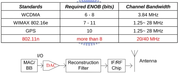
In the recently years, wireless communication standards in [1], such as WCDMA, UMTS, WIMAX 802.16e and 802.11n, require high speed and high resolution digital-to-analog converters.
Table 1.1 Wireless communication standards.
Channel Bandwidth Required ENOB (bits)
Standards 1.25~ 28 MHz 10 GPS WCDMA 6 - 8 3.84 MHz WIMAX 802.16e 7 - 11 1.25~ 28 MHz 802.11n more than 8 20/40 MHz
Standards Required ENOB (bits) Channel Bandwidth
WCDMA 6 - 8 3.84 MHz 1.25~ 28 MHz 10 WIMAX 802.16e 7 - 11 1.25~ 28 MHz GPS 802.11n more than 8 20/40 MHz
Fig. 1.1 DAC application for wireless communication system.
Current-steering DAC is a particularly appropriate architecture for these applications in Table 1.1. This DAC is in which an array of current sources are steered to output resistance depending on digital input code. These DAC’s specification in dynamic performance, such as spurious free dynamic range (SFDR) and signal-to-noise ratio (SNR), are more important than static performances including INL and DNL in wireless communication systems.
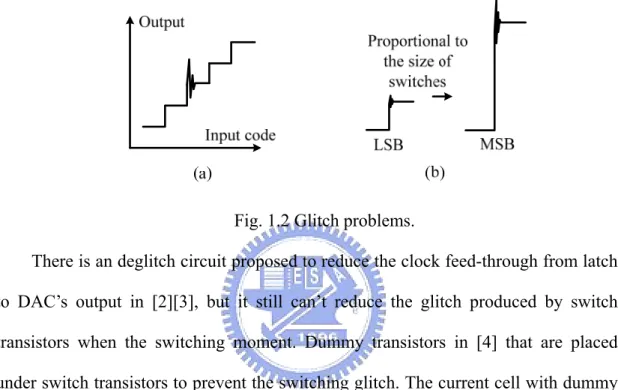
some papers have been presented to eliminate the glitch energy in [2][3][4][5]. The glitch problem associated with current steering architecture is that if the MSB’s current is large, then the width size of switching pair transistors need to be large as shown in Fig. 1.2 (b). So that the pick value of glitch occurs. This thesis has proposed a multi-finger technique to reduce the glitch height in the current cell design.
Fig. 1.2 Glitch problems.
There is an deglitch circuit proposed to reduce the clock feed-through from latch to DAC’s output in [2][3], but it still can’t reduce the glitch produced by switch transistors when the switching moment. Dummy transistors in [4] that are placed under switch transistors to prevent the switching glitch. The current cell with dummy transistors needs high supply voltage to keep every transistor in the current cell work in saturation. The glitch height is reduced in [5], it has presented a “finger-approach” technique to make the switch on or off in the different time. But the slightly different time is tune by delay cell in front of the current cell, may cause more power consum
ithout adding any circuit, so that it needn’t additional power consumption and area.
ption, and hard designed in high speed DAC.
This paper has proposed a “multi-finger” technique to reduce the glitch energy efficiently w
1.2 Organization
This thesis is organized as six chapters. Chapter 2 describes the overview of current-steering DAC at first, then SFDR constrained by switch size of current cell and glitch-reducing method will be discussed.
Chapter 3 explains the non-idealities in the current-steering DAC, including the relation between glitch problems and spectral performance then random and symmetric errors are mentioned. Some paper will be reviewed in this chapter.
Chapter 4 presents the implementation of the DAC. It includes “multi-finger” for reducing glitch and optimal switching sequence for reducing INL. The impact of output impedance on INL and SFDR performance is explained. Then layout of settling time and bias circuit are considered. Finally the simulation results are presented.
Chapter 5 presents the testing setup and measurement results. Conclusions are following by Chapter 6.
Chapter 2
Overview of Current steering DAC
This chapter begins with a brief overview of digital-to-analog converter (DAC) in the aspects of segmented current-steering architecture. Following by the classification of DAC, we discuss the nonlinearity of current-steering DAC.
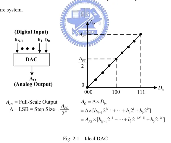
2.1 Ideal Digital-to-analog Converter (DAC)
When a DAC is used in wireless communication applications it is important to know the limitations of the converter and how they affect the performance of the entire system. FS A 2 FS A Full-Scale Output FS A = LSB = Step Size 2 FS N A Δ = = 000 100 111 0 in D O A 1 1 0 1 1 0 1 ( 1) 1 1 0 [ 2 2 2 ] [ 2 2 2 O in N N N N FS N A D b b b A b b b − − − − − − = Δ × = Δ× + + + = × + + + L L − ]
Fig. 2.1 Ideal DAC
Therefore measures to characterize the converters are needed. The DAC viewed as a black box (shown in Fig. 2.1), takes an digital input signal and converts it to a analog output usually in the form of a voltage or a current.
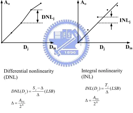
2.2 Static Performance of DAC
Due to non-ideal circuit elements in the actual implementation of a DAC the
digital code transition points in the transfer function will moved as illustrated in Fig. 2.2. The step size in the non-idea data converter deviates from the ideal size Δ and this error is called the differential nonlinearity (DNL) error. For a DAC the DNL can be defined as the following equation since the analog value can be directly measured at the output. In the other way, the total deviation of an analog value from the ideal value is called integral nonlinearity (INL). The normalized INL can expressed as Fig. 2.2.
Differential nonlinearity (DNL) ( ) ( ) 2 j j FS N S DNL D LSB A − Δ = Δ Δ = Integral nonlinearity (INL) ( ) ( ) 2 j j FS N T INL D LSB A = Δ Δ =
Fig. 2.2 Non-ideal DAC’s transfer function.
2.3 Dynamic Performance of DAC
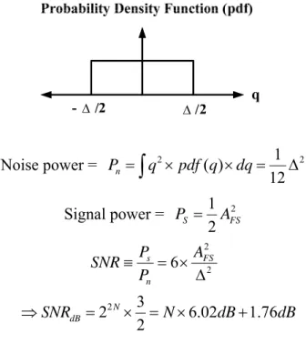
A sinusoidal signal is often used to characterize a data converter. It is therefore interesting to calculate the ideal signal-to-noise ratio of a DAC using such an input signal, q is the quantization process.
Δ Δ Noise power = 2 ( ) 1 2 12 n P =
∫
q ×pdf q ×dq= Δ Signal power = 1 2 2 S F P = AS 2 2 6 s FS n P A SNR P ≡ = × Δ 2 3 2 6.02 1.76 2 N dB SNR N dB dB ⇒ = × = × + (2.1)The spurious free dynamic range (SFDR) is the ratio of the power of the signal and the power of the largest spurious within a certain frequency band. SFDR is usually measured in the FFT spectrum (shown in Fig. 2.3). Its the height between the signal power and largest spurious power. So SFDR can be expressed as (2.2) [18].
Signal Power
10 log( )
Largest Spurious Power
dB
SFDR = × (2.2)
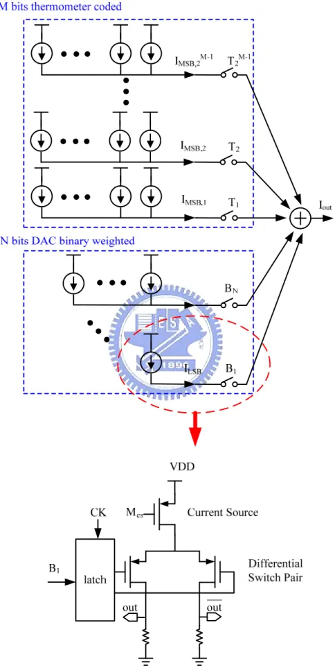
2.4 Segmented Architecture Current-steering DAC
To achieve good monotonicity and reduce the influence of glitches, as well as reducing the sensitivity to matching errors, the DAC should be segmented into a coarse and fine part. The coarse part is thermometer coded and find part is kept binary weighted.
The thermometer ceded DAC architecture means that a number of equally weighted elements. The binary input code is encoded into a thermometer code as illustrated in Table 2.1 for 3-bit input code. With N binary bits, we have M =
thermometer coded bits. The analog output dependent by digital input i :
2N −1 0
( )
M out LSB kI
i
I
k
==
×
∑
(2.5)Table 2.1 Decimal, binary and thermometer code representations.
Decimal Binary weighted Thermometer code
0 000 0000000 1 001 0000001 2 010 0000011 3 011 0000111 4 100 0001111 5 101 0011111 6 110 0111111 7 111 1111111
In the thermometer coded DAC the reference elements are all equally large and the matching of the individual elements becomes simpler than the binary case. The
converter is monotonic and the DNL and INL is improved compared to the binary version. The requirement on element matching is also relaxed. In fact, if the matching is within a 50% margin, the converter is still monotonic [6].
For a high resolution and large number of bits, the digital circuits converting the binary code into thermometer code and the number of interconnecting wires may be occupied large area. This implies a more complex circuit layout.
To trade off the performance and cost, the better choice is a DAC structure where the M most significant bits (MSBs) are thermometer coded and the N least significant bits (LSBs) are binary weighted. This is referred to as a segmented structure and it is illustrated in Fig. 2.4. Each architecture that of the current cells is shown in Fig. 2.4 includes latch, current source and switch pair.
An extension to the segmented structure is to use multi-segmentation. For example, the M MSBs are thermometer coded in one cluster, the K LSBs are kept binary coded, and the N-M-K intermediate bits are also thermometer coded in one separate cluster for example as [6].
out out
2.5 Nonidealities in current-steering DAC
This section discusses defects of actual current-steering DAC caused by glitch, random errors and systematic errors. As following, several papers to overcome above limitation are proposed and detail mechanisms of papers in the recently years.
As mentioned in chapter 1, the glitch causes THD (the best total harmonic distortion) high, so that the SFDR will get worse. The dynamic performance of current-steering DAC is limited by three factors:
Δ 3Δ 2Δ
Fig. 2.5 An actual DAC output signal and the FFT of sine iuput
2.5.1 The imperfect synchronization of the control signals of the
switch pair
This problem can be solved by placing synchronization latches in front of the switches. In this way any different delay introduced by the digital decoding logic circuit can be eliminated. This is to overcome the skew between the row and column select signal. Moreover , special attention has been paid to the layout to ensure that the interconnect capacitance and resistance at the latch outputs are the same value, so that the synchronism is kept as good as possible. However, the logic of the 4 LSB’s is
more difficult to keep synchronism with the MSB’s part.
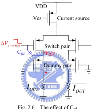
2.5.2 Coupling of the control signals feed-through the C
gdof the
switch pair to the output
The coupling of the switching control signals to the output lines through the Cgd
of the switching transistors is a source of glitches.
OUT
I
OUTI
V Δ g switch V − ΔFig. 2.6 The effect of Cgd
The voltage variation at the DAC output is approximately by
gd g switch gd d tot C V C C − − Δ ≈ Δ + V (3.1)
where Cd-tot is the total parasitic drain capacitance of the switching transistor, then n
number current switch cell the total glitch is nΔV, when n is large, significant
glitches appear at the output of DAC. Furthermore, the glitches dependent on the control signal of the switch transistor, so it is code dependent, they cause harmonic distortion of the DAC input signal.
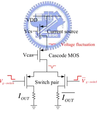
2.5.3 Drain voltage fluctuation of the current source transistors
Ideally, the voltage at the drain node of current source transistor should be constant to produce stable current. In the conventional switch driver, both switches may be simultaneously in the off-state for a short period of time, so the current source transistor will enter the linear region. Therefore a large voltage variation at this node can manly degrade the DAC’s dynamic performance.
A popular circuit solutions is to isolate the drain node of the current source by using cascode transistor. This solution is effective, however , provided that cascode transistor remain in saturation. Furthermore, because of the limited power supply
voltage, the current source gate voltage overdrive must be reduced by the Vd-sat
voltage of the cascode transistor.
OUT
I
OUTI
Vcs Vcas VDD Switch pair Current source Cascode MOS Voltage fluctuation g switch V − g switch V −Fig. 2.7 The effect of voltage fluctuation
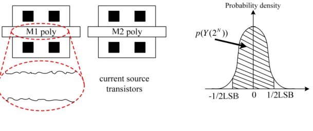
2.6 Current Source Random Error
Matching current sources suffer a finite mismatch due to uncertainties in each step of the manufacturing process. The random variation is modeled using a normal
( (2 ))N
p Y
Fig. 2.8 Random error and its normal distribution
. From [7], for 10 bit resolution we require 99.7% yield to achieve INL
specification (<0.5LSB) ,so σ( )I I is about 0.5%.
1/ 2 1/ 2
( (2 ))
(2 )
( (2 ))
(2 )
LSB N N C N LSBp Y
dY
Cp Y
dY
σ σ −=
−∫
∫
N0.5
2
yieldINL
=
+
_ _ 0.5 2 INL yield C =inv norm⎛⎜ + ⎞⎟ ⎝ ⎠ 2 1 2N I I Cσ
+ ⎛ ⎞ ≤ ⎜ ⎟ ⎝ ⎠ •2.7 Current Source Systematic Errors
For DAC with a resolution of 10-bit and higher, the dimensions of the current source array become so large that process, temperature, and electrical gradients have to be considered. A radial pattern in the oxide thickness which gives rise to a shift values in the current source array approximately linear with the devices separation distance. Temperature gradients and stress gradients are responsible for errors approximately parabolic across the array matrix as shown in Fig. 2.9.
-1 -0.5 0 0.5 1 -1 -0.5 0 0.5 1 0 0.2 0.4 0.6 0.8 x direction y direction N o rm al iz ed s y s tem at ic err or 0 0.05 0.1 0.15 0.2 0.25 0.3 0.35 0.4 0.45 0.5 -1 -0.5 0 0.5 1 -1 0 1 -0.4 -0.2 0 0.2 0.4 x direction y direction N o rm a lize d syst e m a ti c e rr o r -0.25 -0.2 -0.15 -0.1 -0.05 0 0.05 0.1 0.15 0.2 0.25
2.8 Review of Current Steering DAC
There are many papers presented in the recently years as shown in Table 2.2. Here we take attention on glitch problem which is focused by some papers. [7] is the comparison with my goal.
Table 2.2 Specification of current-steering DAC papers in the recently years
Year Tech (um) (bit) Res Segmen- tation Update rate (LSB)DNL (LSB)INL SFDR(dB)
Area (mm2 ) Power (mW) FOM (pJ) 2005 [12] 0.35 12 7+5 MS/s250 0.25 0.5 74 N/A 66.5 0.103 2006 [5] 0.35 16 7+6+3 MS/s50 0.1 0.3 77 0.06 165 1.8 2006 [13] 0.35 12 8+4 MS/s300 0.5 0.6 62 3.52 150 1.161 2007 [7] post-sim ulation 0.09 10 6+4 400 MS/s 0.15 0.17 55 @ 40M/ 400M 0.28 23 0.16 @ 40M/ 400M 2004 [10] 0.18 12 7+5 MS/s320 0.3 0.4 64 0.44 82 0.579 2007 [14] 0.18 14 14+0 MS/s150 1 3.5 77 3.0 127 0.462 2006 [15] 0.18 14 14+0 MS/s200 0.57 0.76 78 3.0 210 0.513 2007 [16] 0.18 14 11+3 MS/s200 0.91 1.51 83.5 0.65 59.3 0.176 ENOB sampling POWER FOM= 2 ×f (3.5)
2.8.1 Deglitch and low power latch
The glitch problem has great effect upon the dynamic performance of current-steering DAC. The synchronization of control signals of the switches and the voltage variations at the drain of the current source transistors. Generally, the latch which is placed in front of the current cell can be seen as a driver. It performs the final synchronization and adjusts the crossing point of the differential output of control signals.
This has presented a latch as shown in Fig. 2.10 in [7] which reduces power glitches and dynamic power consumption because there is no dc current path from
VDD to GND. For PMOS current switch used in this design, the differential output
control signals of the latches must have a low crossing point to prevent switch transistors from being simultaneously turned off.
in
D
in
D
Fig. 2.10 Low power and low glitch latch
2.8.2 Dummy transistors for preventing glitch
For minimizing the feedthrough to the output lines, the drain of the switching transistors is isolated from the output lines. This thesis adds two cascaded transistors (with the same dimensions as the switching transistors), as shown in Fig. 2.11 in [4].
For a high-to-low transition of the control signal, while the switching transistor is forming a channel, the cascaded transistors are off and the signal path from the drain of the switching transistor to the output node is open. The coupling is therefore avoided. For a low-to-high transition some coupling exists at the beginning, but since the switching transistor cuts off very rapidly the voltage at the source of the cascade transistor drops, turning it off, and isolating the output node for the remaining of the transition of the control signals.
OUT
I
OUTI
Fig. 2.11 The current cell with dummy transistors
2.8.3 Finger approach for reducing glitch
the glitch height, but does not completely remove this glitch.
[5] MSB current cell requires a relatively large size of the switch to pass this large current. But due to overlap capacitance, there occurs a glitch. When it changes from off to on state. To reduce this glitch, a novel approach is used. In this approach, the large dimension of switch is split into different small switches. The gate inputs of these switches are progressively delayed by an optimum delay (Fig. 2.12). This reduces the height of the glitch, because it splits the big glitch into different small glitches. Finger approach definitely reduces
Fig. 2.12 The current cell with finger approach
2.9 Summary
There is an deglitch circuit proposed to reduce the clock feed-through from latch to DAC’s output in [2][3], but it still can’t reduce the glitch produced by switch transistors when the switching moment.
Dummy transistors in [4] that are placed under switch transistors to prevent the switching glitch. The current cell with dummy transistors needs high supply voltage to keep every transistor in the current cell work in saturation.
The glitch height is reduced in [5], it has presented a “finger-approach” technique to make the switch on or off in the different time. But the slightly different time is tune by delay cell in front of the current cell, may cause more power consumption, and hard designed in high speed DAC.
This paper has proposed a “multi-finger” technique to reduce the glitch energy efficiently without adding any circuit, so it needn’t additional power consumption and area.
Chapter 3
Reducing The Glitch Energy
Most current-steering DACs are implemented using a segmented architecture in [5] as shown in Fig. 3.1 includes N bits binary-weighted current sources and M bits unary current cell which are the equally weighted in thermometer part.
W L W L+ ΔL W L+ ΔL W L
Fig. 3.1 “N + M” segmented current steering DAC
The main glitch is caused by MSB part (thermometer DAC) which requires a
relatively larger size of the switching transistors. MSW, MSB pass this larger current.
However, due to overlap capacitance, when switches are in the switching moment then the worst case of glitch occurs. This paper present a special technique called “multi-finger” which make the MSB’s switch transistors finger into two transistors which have slightly different length, so the switches will trigger non-simultaneously to reduce the glitch energy.
3.1 SFDR Constrained by Switch Size of Current Cell
The SFDR is constrained by two conditions: the first is the gain of switch
transistors; the other is the delay difference (dmax) of output net of DAC.
The current cell can achieve an improved bandwidth up to the Nyquist frequency in [8]. There is a relationship between the required output impedance and SFDR specification is given by
(1 2 )
4
4
L L requiredNR
Q
NR
R
Q
Q
−
=
≈
(3.1)where Q is the ratio between the fundamental signal and the second harmonic component (Q can be seen as SFDR).
g,sw
V
Vg,sw VDD MCS MCAS MSW MSW RL RL O V ( )t O V ( )tFig. 3.2 The basic current cell
Besides, the gain of switch transistor has to be larger than the given equation (3.2) otherwise the non-linearity introduced by the output impedance of the DAC make a hard constraint on the dynamic specification.
0
2
0msw sw N required
where fN is the Nyquist frequency, C0 is the total capacitance at the drain of the
current source. Combine (3.1) (3.2) condition.
0
2
04
L msw sw NNR
g
r
f C
Q
π
≥
where2
p m o DK
g r
WL
I
λ
= ×
⇒ 02
2
p L N DK
NR
WL
f C
I
π
Q
λ
×
≥
⇒ 04
L D N pNR
I
WL
f C
Q
K
π
λ
≥
×
(3.3)We can get a relationship between switch size and SFDR for gain condition.
On the other way, there is an issue about the delay difference on the output net in
[9]. We call the delay dmax in this thesis. The dmax influences the SFDR as the equation
(3.4). 2 2 2 2 max max
1 8
4
( )
1 2
2
2
cos(
)
in in in in in in ckf
F f
f
SFDR
f
rd
d
w
d
f
f
π τ
π τ
π
π
+
+
=
=
≈
Δ
(3.4)where Δ2rd is the second harmonic, fin is input frequency, fck is sampling frequency.
For current-steering DAC, the switches are driven by latches. Normally the slew
rate of the latches determines the transition time Tsw. As a simply approximation, if
the gate capacitance of the switch transistor is Csw, then the transition time can be
expressed as , g sw sw sw D
V
C
T
I
×
=
Fig. 3 shows the waveform of the control signal Vg,sw. Tsw is the transition time of
control signal. Vd,sw is the drain voltage of the switch transistor, Vo,pp is the
peak-to-peak value of the output voltage. Vd,sw is the 1/ (1+gmro) ratio of Vo,pp. The
factor Vg,sw/Tsw is the switching speed. We can see that the dmax can be expressed as
, max , , ,
(
)
(
1
o pp sw sw d sw)
g sw m o g swV
T
T
d
V
V
g r V
=
=
+
(3.5) take (3.5) in (3.4) equation ⇒4
o pp, ox in ox P DV
WL
f
SFDR
t
K
I
ε
λ
≤ ×
×
×
×
×
(3.6)The intrinsic idea of this method is to increase the size of switch transistor to improve the SFDR specification. max
d
swT
g,swV
d,swV
Fig. 3.3 Transition of the control signal of switch (MSB)
3.2 Multi-finger Technique
The optimal solution of switch size must satisfy the (3.2) for gain condition and
(3.6) for dmax condition as shown in Fig. 3.4. The W*L is taken A to achieve best
0.2 0.4 0.6 0.8 1 1.2 1.4 1.6 60 65 70 75 80 85 90 95 100 WxL (um2) S F D R (dB )
for dmax condition for gain condition
Fig. 3.4 SFDR constrained by switch size
In this thesis, we especially finger MSB’s switch into two transistors and tune the length of them slightly different to make the switch on or off non-simultaneously as equation (3.7).
(
)
(
)
*(
2
2
W
W
A
L
L
L
W
L
)
2
L
Δ
=
∗ +
+ Δ =
+
(3.7)Besides, full scale current of DAC has been decided at first, then the MSB’s current of unary cell in thermometer part is the M times of LSB’s current in binary
part. So that to keep the same Vov of switch transistor for every current cell of all
DAC. _ 2
1
*
*(
)
2
2
1
full scale LSB P ox ov NI
W
I
C
V
L
μ
=
=
−
*
( )
*( )
MSB LSB MSB LSBW
W
I
M I
M
L
=
⇒
=
L
(3.8)From the equations (3.7) and (3.8), we can get the only solution of L to design the different switching time for reducing glitch energy in the derivation in (3.9) and as
shown in Fig. 3.5. The glitch energy is proportional to the switch size, if the finger transistor can on or off non-simultaneously. The glitch energy will be reduced approximately half.
*
(
2
LSB)
L
A
=
M W
L
+
Δ
(3.10) 1 * W LChapter 4
DAC Implementation
In this chapter, to verify the method of reducing glitch energy, we have proposed a segmented architecture includes 4 bits LSBs binary-weighted DAC and 6 bits MSBs thermometer part as shown in Fig. 4.1. multi-finger is proposed at first and each component will be design as following, infinite output impedance and layout consideration are the important issues in the DAC design. Finally, the simulation results are presented at last.
Input Registers Local Decoder + Latches Array Switch Pair + Cascode Array Binary to Thermometer Delay Equalizer
Current Source Array Bias Clock 50Ω 50Ω Iout IoutB Local Decoder + Latches Array Switch Pair + Cascode Array MCS MCAS W L W L+ ΔL W L+ ΔL W L RL MSW1 MSW2 RL
4 bits binary 6 bits thermometer
Fig. 4.1 “4 + 6” segmented current steering DAC
4.1 Multi-finger For Reducing Glitch
As Chapter 3 mentioned, the constant A of this design is 0.54um2. M = 24 for this
simply calculating, we can get the only solution for ΔL = 0.18um. The fingered size of MSB’s transistors is listed in Table 4.1.
Table 4.1 : The finger size of MSB’s switch transistors
MSW1 MSW2
Width 1um 1um
Length 0.18um 0.18um+0.18um
4.2 The Digital Circuits
Fig. 4.2 shows the digital circuits which are perform in the front end of DAC. First, the 10-bit input signal need to synchronize by the registers. Then the input binary codes of 6-MSBSs are converted into 63 bits thermometer codes. Because the 6-to-63 decoder circuits are complicated, we divide it into row-and-column which are two 3-to-7 thermometer codes. All the signals from the binary-to-thermometer circuits feed into the local decoders in the same time to control the 63 latches. A delay equalizer in the binary-weighted path is used to eliminate the different delay time between the control paths in the MSB and LSB part.
Fig. 4.3 (a) is the schematic of 3-bit to 7-bit thermometer code. Fig. 4.3 (b) is the wave form of the thermometer code.
T1=b1+b2+b3 T2=b2+b3 T3=b1 b2+b3•
T4=b3
T5=(b1+b2) b3• T6=b2 b3• T7=b1 b2 b3• •
(a) schematic
(b) simulation of binary to thermometer code Fig. 4.3 3bits binary to 7 bits thermometer code Symbol Wave D0:tr0:v(t1) D0:tr0:v(t3) D0:tr0:v(t4) D0:tr0:v(t5) D0:tr0:v(t6) D0:tr0:v(t7) D0:tr0:v(t2) Voltages ( 0 500m 1 Voltages ( 0 500m 1 Voltages ( 0 500m 1 Voltages ( 0 500m 1 Voltages ( 0 500m 1 Voltages ( 0 500m 1 Voltages ( 0 500m 1
Time (lin) (TIME)
0 5n 10n
Panel 1
4.3 The High-Speed Latch
We place a latch in front of the current cell. The 4bits binary-weighted and 63bits thermometer codes differential signals that produced from the local decoder are finally synchronized to control the current cell in the same time. Second, when the latch’s differential output signals operates in the crossing point which is in the middle of supply voltage. The switch pair will turn off simultaneously, so that the current-source transistor will work in the linear region. The voltage fluctuation occurs on the drain node of the current-source transistor.
Fig. 4.4 shows the schematic of the latch in this design [10]. For PMOS current cell used in this thesis, the low crossing point is needed to prevent the switch pair turn off simultaneously. Two extra NMOS transistors (M5a, M5b) are placed in the parallel with each of the cross-coupled NMOS. M5a, M5b perform the fall time is much faster than rise time of the driver circuit. In this way, a low crossing point of the differential outputs is available at the output of the latch. The additional feedback by the inverter pair suppresses the clock feedthrough which is produced by the pass transistor and stabilizes the synchronized input signals. Fig. 4.4 (c) shows the wave form of the latch. IN D IN D OUT OUT (a) schematic
DVDD 2 OUT OUT OUT OUT OUT OUT
(b) differential output signals
(c) simulation of differential output Fig. 4.4 The high speed latch
4.4 Output Impedance Analysis
The impedance at the DAC’s output node in Fig. 4.6 (a) is determined by a
parallel circuit of the unity current switch cell. As generally known, the Zimp seen in
DAC’s output needs to be made large so that its influence on the INL specification of the DAC is negligible. The relation between the Zimp and achieved INL specification (< 0.5 LSB) is given (4.1). 2 2 4 unit L imp I R N INL R = (4.1) Symbol Wave D0:tr0:v(q) D0:tr0:v(qb) Voltages (lin) 0 100m 200m 300m 400m 500m 600m 700m 800m 900m 1000m
Time (lin) (TIME) 4n
Panel 1
where RL is the load resistor, Iunit the LSB current, and N the total number of unit
current sources.
To design a sizing strategy in current cell is important with the 1.8V analog
supply voltage. First, the aspect ratio W/L fixes the overdrive voltage (VGS-VT) for
each transistor and for a given current . The optimal aspect ratio can be found to give
MCAS and MSW more rest in headroom, most important, we must consider the output
swing and output impedance.
For DAC static requirement INL < 0.5 LSB, take the parameters RL = 50 N =
1024 into (4.5) → ro > 1.31GΩ
For SFDR =70dB to satisfy the wireless communication specification in, take the
parameters N = 2b (b = DAC resolution) into (4.2) → ro > 367MΩ
20 log
o6(
2)[
]
Lr
SFDR
b
dB
R
=
−
−
(4.2)For above INL and SFDR conditions, for INL/SFDR required
ro = (gm3+gmb3)(gm2+gmb2)ro3ro2ro1 = 2.097 GΩ > 1.31 GΩ
Fig. 4.12 shows the LSB differential output current which is 4.2uA.
Q V Q V out out (a) schematic
(b) simulation of differential output Fig. 4.5 The LSB current cell
4.5 Random Errors
In chapter 2.6, to achieve the static specification that INL must be less than 0.5
LSB in 3σ. We can get σ( )I I is about 0.5% in the 10-bit resolution DAC. According
to these results and the required area versus matching relation for current source transistor (Mcs) . The minimum area of a unit current source transistor is given by
2 2 GS T min 2 I [A 4A /(V V )] 1 (W L) 2 ( /I) VT β σ + − × =
Fig. 4.5 shows the curve above equation. In the design, the p-type transistor is more
suitable than n-type transistor. Because Aβ and AVT of p-type are less than these in the
n-type, smaller area of transistor can be implemented. Symbol Wave D0:tr0:i(r1) D0:tr0:i(r2) Currents (lin) -500n 0 500n 1u 1.5u 2u 2.5u 3u 3.5u 4u
Time (lin) (TIME)
0 1n 2n 3n 4n 5n
*** 1unit current switch latch ***
0.1 0.2 0.3 0.4 0.5 0.6 0.7 0.8 0 10 20 30 40 50 60 70 80 90 100 Overdrive voltage (VGS-VT) of M1 [V] Un it c ur rent s our c e ar ea [ u m 2] PMOS NMOS
Fig. 4.6 Unit current source area vs. its overdrive voltage
From Fig. 4.5, it is obvious that increasing the overdrive voltage reduces the area consumed. However, this value of overdrive voltage is limited by the headroom of Mcas and switch transistor. Consider the current switch headroom for 1.8V supply
voltage, we take the VGS,min. For required output impedance, these transistors in the
current cell must operate in the saturation region.
4.6 Systematic Errors
Systematic errors include parabolic error and linear error. The well known that row-column switching scheme is commonly used to eliminate the parabolic error. Its advantage is the simplicity for design and layout, especially reduce the routing between current cell and local decoder, so that a lot of area can be saved.
Fig. 4.7 The linear and parabolic error distribute in the current source array In this scheme, the parabolic errors are averaged in two directions. In each cell, the area occupied by the local decoder, switches and cascode transistors is often comparable to the active area, a possible way to reduce the source array area and the distances between elements, is to move all the other transistors from the array besides current source transistors.
4.6.1 Parabolic error compensation
First, we build a model of parabolic error as seen in Fig. 4.6. This optimal sequence can be found by tree structure in [11] (Fig. 4.6). The algorism is that to achieve lowest magnitude of error in 1x8 or 8x1 unary array. For 6 MSBs thermometer code, a 1×8 unary array with parabolic error is given in Table 4.1.
Three switching scheme are consider, first one is the sequential scheme and second is conventionally common-centroid, last is a optimal switching scheme presented by tree structure. Column 1 and 2 show the actual values of the elements in
the array and the relative error of each element. For example, with the common-centroid sequence, as the digital input increases from 1 to 8, the element with error -3% is switched on first and number 1, the element with error -3% is switched on next and numbered 2, and so forth. INL of the DAC can be calculated as shown in the last 2 columns of Table 4.1. The common-centroid sequence results in an INLDAC of 8% due to sever error accumulation. New switching scheme can further reduce the error by a factor of four.
Table 4.1 Switching schemes. (a) common-centroid (b) new switching scheme
The optimal sequence given in Table 4.1 is not unique. There are several other optimal sequences, two of which are obtained if the elements in the array (from the left to the right) are numbered 2 4 8 6 3 1 5 7 and 3 1 5 7 2 4 8 6.
4.6.2 Linear error compensation
As shown in Fig. 4.8, to suppress the linear erorr, some methods are that separating biasing for each quadrant of the current matrix, and splitting each current source into four units of quarter value. So that the 63 unit current source of the 6 MSBs are located in four symmetrical sub-matrix. All the digital circuits and interconnections between the switching matrix array and current sources array are put on top of the chip.
Fig. 4.8 The quarter symmetric and new switching scheme
4.7 Settling Time Condition
To obtain the settling time requirement, we use the single pole approximation to model the output node as shown in From Fig. 4.13. The worst case settling time
within 1/2LSB is derived as (4.3) and (4.4). To meet the specication in this work, we set M=10 and tsett = 2ns, such that the upper bound of equivalent capacitance value at
output node to be 5.25pF when off chip RL = 50.
O L
for R >>R
(1
tsettT)
O LV
= ×
I
R
−
e
− (4.3) 1 L I L1
(1
)
(1
)
2
(
1) ln 2
where T = R (C +C )
sett t T L L M settI
R
I
R
e
t
T M
− +−
×
= ×
−
→
=
+ ×
(4.4)Fig. 4.9 Single pole approximation model for current cell
4.8 Bias Circuit
Fig. 4.10 shows the biasing scheme for the cascoded current sources. An internal resistor is used to generate the reference current. The NMOS sections of the biasing circuits are as “global biasing” while the PMOS sections are labeled as “local biasing.” In the actual implementation, the global biasing is realized using a common-centroid layout to reduce effects of gradients. The local biasing is separated into four quadrants. There is no direct connection between any two quadrants as shown in Fig. 4.10 (b).
(a) schematic
(b) floor plan of global and local bias Fig. 4.10 Bias circuit
4.9 Simulation Results
Pre-layout simulation Results
The static specification DNL/INL need less than 0.5LSB to achieve accurate required. Pre-simulation results is in the condition of (fin/fck = 250M/500M), and shown in Fig. 4.11, DNL = 0.03LSB, INL = 0.042LSB. SFDR is 80 dB @ fin/fck = 50MHz/ 500MHz. 0 200 400 600 800 1000 1200 -0.04 -0.02 0 0.02 0.04 input code D N L ( L SB) 0 200 400 600 800 1000 1200 -0.04 -0.02 0 0.02 0.04 0.06 input c ode IN L ( L S B )
Fig. 4.11 Pre-layout simulation for (a)DNL (b) INL
0 0.5 1 1.5 2 2.5 x 10⁸ -120 -100 -80 -60 -40 -20 0 Frequency [Hz] O u tput s p ec tr um [ dB ] X: 8e+007 Y : -79.58
Version 1 of Layout Diagram
This thesis is implemented in TSMC 0.18um 1P6M CMOS technique, the layout
of core area is 0.25mm2 and 0.58mm2 with PAD. The layout diagram is shown in Fig.
4.13.
The static specification DNL/INL need less than 0.5LSB to achieve accurate required as shown in Fig. 4.14. DNL = 0.25LSB, INL = 0.27LSB.
Fig. 4.13 Version 1 of Layout Diagram
0 200 400 600 800 1000 1200 -0.2 -0.1 0 0.1 0.2 0.3 input code DNL ( L S B ) 0 200 400 600 800 1000 1200 -0.2 -0.1 0 0.1 0.2 0.3 input code IN L ( L SB)
The 2048-point FFT of the post-simulation result is shown as Fig. 4.15 (a) 55dB @ fin/fck = 1MHz/500MHz, SFDR (b) SFDR is 47 dB fin/fck = 250MHz/500MHz 0 50 100 150 200 250 -120 -100 -80 -60 -40 -20 0 Frequency [MHz] O u tp u t sp e c tr u m [d B ] X: 214.9 Y: -56.02 0 50 100 150 200 250 -120 -100 -80 -60 -40 -20 0 Frequency [MHz] Out put s pec tr um [ dB ] X: 18.52Y: -46.96
Fig. 4.15 Post-layout simulation for Version 1 of SFDR
The package type is LCC type 68 pins where the actual chip photograph is shown at Fig. 4.16.
Fig. 4.16 Version 1 of die photograph
The specification of post-layout simulation drop a lot by compared with pre-layout simulation. The main question is the parasitic capacitors between switch pair and the output node. There are 4+63 metal lines that connect to the switch pairs and output node .Those capacitors cause the timing skew and non-synchronization. So,
we need short the connecting line to get small capacitor.
The other problem is the input buffer consideration. The measurement of version
1 is presented in Chapter 5
To solve above two problems, we design the version 2 of layout diagram which includes minimizing metal line between each current cell and output node and adding input buffer in the front of DAC core circuit.
Version 2 of Layout Diagram
The version 2 of layout diagram is shown in Fig. 4.17. The ESD pad is used in
this version. The metal of each current cell output is minimized to reduce the non-equal capacitors. We have add the input buffer to drive the input loading. The
core area is only 0.175mm2 and 0.65mm2 with ESD pad.
Fig. 4.17 The layout diagram of 10 bits DAC
Multi-finger Technique
The peak value of the glitch in a DAC’s output as it switches across the largest major transition (0111111111→ 1000000000). Glitch energy definition : 0.5*(glitch_height)*(impulse_time) in [2][3]. The post layout simulation shows that the glitch energy are 0.77pVs without multi-finger and 0.4pVs with multi-finger as shown in Fig. 4.18.
Fig. 4.18 Glitch energy (a) without “multi-finger” (b) with “multi-finger” 10 bits ramp digital is applied to the input, and the output of DAC (Fig. 4.19) is recoded to calculate DNL/INL with MATLAB tool. We can adjust the static performance well or not by the glitch produced in the signal transition.
Fig. 4.19 Differential symmetric ramp code of DAC output
INL and DNL as shown in Fig. 4.20 are less than 0.07 and 0.06 LSB, these
results achieve the static requirement.
0 200 400 600 800 1000 1200 -0.1 -0.05 0 0.05 0.1 input code DNL ( L S B ) 0 200 400 600 800 1000 1200 -0.05 0 0.05 0.1 0.15 input code IN L ( L SB)
Fig. 4.20 Post layout simulation for static performance
The SFDR as shown in Fig. 4.13 for a 49M pling rate
(a) DNL <0.06LSB (b) INL <0.07LSB
Hz signal at a 500MHz sam
is about 74dB, this specification can satisfy required wireless communication. The summary of the performance of the proposed DAC is show in Table 2. In the near future, the chip will be fabrication and testing the chip performance.
Symbol Wave D0:tr0:i(ro1) D0:tr0:i(ro2) Currents (lin) -500u 0 500u 1m 1.5m 2m 2.5m 3m 3.5m 4m 4.5m
Time (lin) (TIME)
0 500n 1u 1.5u
Panel 1
0 0.5 1 1.5 2 2.5 x 10⁸ -120 -100 -80 -60 -40 -20 0 Frequency [Hz] O u tp u t sp e ctr u m [ d B ] X: 1.418e+008 Y: -74.42
Fig. 4.21 Post layout simulation of SFDR
(a) fin/fck /500MHz
4.10 Summary
ary of the DAC version 2 post-layout simulation = 49MHz/500MHz (b) fin/fck = 247MHz
Table 4.2. Summ
[2] APCCAS [3] ISSCC This thesis
version 2
Techn logy o 0.25-μm 0.18-μm 0.18-μm
Resolution 10-bit 10-bit 10-bit Sampling rate 300 MHz 250 MHz 500MHz Glitch energy 15pVs@ fck=300MHz 2.64 pVs @ fck=250MHz fck=500MHz 0.4pVs @ DNL < 0.1 LSB < 0.1 LSB < 0.06 LSB INL < 0.1 LSB < 0.1 LSB <0.07 LSB SFDR (3MHz/300 (49MHz/250 (49MHz/500 59dB MHz) 63dB MHz) 74dB MHz) Power consumption 84mW 22mW 14mW active area 1.56 mm2 0.35mm2 0.175mm2 chip area 0.65mm2
ENOB
sampling
POWER FOM=
2 ×f (4.5)
Fig. 4.22 shows the performance of the version
shows that the post-simulation result is the lowest compared to the references. The power consumption is also the lowest.
2 posim in this thesis. The FOM
0 0.2 0.4 0.6 0.8 1 1.2 1.4 1.6 1.8 2 [4] 0 0 200 300 400 500 clock frequenc ) FO M (p J) [3] [4] [5] [6] : intrinsic
[7] [8] : dynamic element matching (DEM) [9] [10] : calibration [5] [3] [7] [6] [8] [9] [10]
this work presim this work posim posim
presim posim presim
Fig. 4.22 FOM vs clock frequency
10
Chapter 5
Testing Setup and Measurement Results
In the chapter, we describe the testing environment, and the version 1 measurement results will be presented as followed. Finally, there is a discussion about the reasons of performance decay at last.
5.1 Measurement Setup
Fig. 5.1 shows PCB layout. The differential output of the DAC is connected by the RF transformer T1-6T (differential -to-single) to produce the single out signal. This measurement include chip with package and without package. The capacitor on
the PCB is used to stable the differential voltage between VDD and GND.
Mini_circuit RF transformer T1-6T (single-to-differential ) : 4M~300MHz
Stabling capacitors for VDD/GND : 0.1u, 1u and 10uF
PCB layout with LCC 68 pins package
Fig. 5.2 Test Setup
Fig. 5.2 shows overall of the measurement setup, In the this setup, all of the input digital code is generated by Agilent 16902B logic analysis system. Agilent 54641D oscilloscope is used to measure the waveform of output and recode the voltage data. Apply 10-bit ramp wave ex : fin/fck = 50M/100M (Fig. 5.3), we can catch the data and calculate DNL/INL by Matlab.
Fig. 5.3 Ramp wave shown in oscilloscope
To measure SFDR, we apply 10-bit digital sine code and output is connected to Agilent E4407B which can calculate the FFT in frequency domain.
Fig. 5.4 Sine wave of DAC output
5.2 Measurement Results
Fig. 5.5 shows the DNL/INL in the 1M/100M and 50M/100M frequency, when operating in 50M/100M, the DNL/INL is larger than 0.5LSB (out of static
performance required). Fig. 5.5 shows the DNL/INL performance in different frequency. 0 2 0 0 4 0 0 6 0 0 8 0 0 1 0 0 0 1 2 0 0 - 0 . 4 - 0 . 3 - 0 . 2 - 0 . 1 0 0 . 1 0 . 2 0 . 3 0 . 4 0 . 5 0 . 6 i n p u t c o d e D N L ( L SB) 0 2 0 0 4 0 0 6 0 0 8 0 0 1 0 0 0 1 2 0 0 - 0 . 6 - 0 . 5 - 0 . 4 - 0 . 3 - 0 . 2 - 0 . 1 0 0 . 1 0 . 2 i n p u t c o d e IN L ( L SB) 0 2 0 0 4 0 0 6 0 0 8 0 0 1 0 0 0 1 2 0 0 - 1 0 1 2 3 4 5 i n p u t c o d e IN L ( L SB) 0 2 0 0 4 0 0 6 0 0 8 0 0 1 0 0 0 1 2 0 0 - 1 . 5 - 1 - 0 . 5 0 0 . 5 1 1 . 5 2 2 . 5 3 i n p u t c o d e DN L (LS B )
DNL = 2.6 LSB @ fin/fck = 50M/100M INL = 4.5 LSB @ fin/fck = 50M/100M
DNL = 0.51 LSB @ fin/fck = 1M/100M INL = 0.52 LSB @ fin/fck = 1M/100M
Fig. 5.5 DNL/INL in measurement
Fig. 5.6 shows the SFDR in the 1M/100M, 41M/100M, 1M/300M and 50M/100MHz are 50dB, 17dB, 36dB and 11.4dB. Fig. 5.7 shows the SFDR in different (fin/fck). The performance drop in the high frequency of input, the reason will be discussed at last.
fin/fck=1M/100M, SFDR=50.34dB fin/fck=1M/300M, SFDR=36.07dB fin/fck=41M/100M, SFDR=17.03dB fin/fck=49M/300M, SFDR=11.46dB Fig. 5.6 SFDR in measurement SFDR vs fin 0 10 20 30 40 50 60 0.1 1 10 100 fin (MHz) SFD R (d B) fck=50MHz fck=100MHz fck=300MHz DNL vs fin 0 0.5 1 1.5 2 2.5 3 3.5 4 0.1 1 10 100 fin (MHz) DN L ( L S B ) fck = 50MHz fck = 100MHz fck = 300MHz INL vs fin 0 1 2 3 4 5 6 0.1 1 10 100 fin (MHz) IN L (L S B ) fck = 50MHz fck = 100MHz fck = 300MHz
5.3 Summary
Fig. 5.9 shows the version 1 of DNL, INL and SFDR performance. When the input frequency move up, and performance get worse. This is the layout question which are no buffers in the input of DAC.
Because of the input driving ability is finite in the HSPICE. In actual, the input driving ability is infinite by the device of LNA (Fig.5.8). Input pad must use digital pad (ESD) and add buffer in front of the core circuit to prevent 10-bit input signal skew. There should be clock tree buffer to ensure each duty cycle of clock is 50% and not skew. The same blocks of digital circuit should be layouted together and different blocks need to be layouted hierarchical. Digital circuit can be save large area by shorting the interconnect from each blocks. The posim with buffer has be shown in Fig. 5.9 and the data of performance is collected in Fig. 5.10.
Fig. 5.8 Actual input driving Symbol Wave D0:tr0:v(bit1) D0:tr0:v(bit2) D0:tr0:v(bit3) D0:tr0:v(bit4) D0:tr0:v(bit5) D0:tr0:v(bit6) D0:tr0:v(bit7) D0:tr0:v(bit9) D0:tr0:v(bit10) D0:tr0:v(ck) D0:tr0:v(bit8) Voltages (lin) 0 100m 200m 300m 400m 500m 600m 700m 800m 900m 1000m
Time (lin) (TIME)
3n 4n 5n 6n 7n 8n
Panel 1
Post-layout Simulation with Input Buffer
0 200 400 600 800 1000 1200 -0.5 0 0.5 1 1.5 2 2.5 3 input code DNL ( L S B ) DNL = 2.5LSB 0 200 400 600 800 1000 1200 -1 0 1 2 3 4 5 input code IN L ( L SB ) INL = 4LSB (a) DNL / INL 0 50 100 150 -90 -80 -70 -60 -50 -40 -30 -20 -10 0 Frequency [MHz] O ut put s p ec tr um [ dB ] 0 5 10 15 20 25 30 35 40 45 50 -100 -90 -80 -70 -60 -50 -40 -30 -20 -10 0 Frequency [MHz] O ut put s pec tr um [ d B ] 0 10 20 30 40 50 -120 -100 -80 -60 -40 -20 0 Frequenc y [M Hz ] O ut p ut s pec tr um [ dB ] fin / fck = 1M/100M SFDR = 50dB fin / fck = 47M/100M SFDR = 23dB 0 50 100 150 -80 -70 -60 -50 -40 -30 -20 -10 0 Frequency [MHz] O ut put s pec tr um [ dB ] fin / fck = 1M/300M SFDR = 37dB fin / fck = 50M/300M SFDR = 15dB (b) SFDRDNL vs fin @ fck = 100MHz 0 0.5 1 1.5 2 2.5 3 1 10 100 fin (MHz) DN L ( L S B ) presim posim measurement posim with buffer
INL vs fin @ fck = 100MHz 0 0.5 1 1.5 2 2.5 3 3.5 4 4.5 5 1 10 100 fin (MHz) INL (L S B ) presim posim measurement posim with buffer
SFDR vs fin @ fck = 100MHz 0 10 20 30 40 50 60 70 80 1 10 100 fin (MHz) S F D R (d B) presim posim measurment psoim with buffer
(a) fck = 100MHz DNL vs fin @ fck = 300MHz 0 0.5 1 1.5 2 2.5 3 3.5 4 1 10 100 fin (MHz) DNL ( L S B ) presim posim measurement posim with buffer
INL vs fin @ fck = 300MHz 0 1 2 3 4 5 6 1 10 100 fin (MHz) INL (L S B ) presim posim measurement posim with buffer
SFDR vs fin @ fck = 300MHz 0 10 20 30 40 50 60 70 80 1 10 100 fin (MHz) SF DR ( d B ) presim posim measurment psoim with buffer
(b) fck = 300MHz
To measure power, we use the source meter to supply the power and record the current into the chip. Power consumption : 1.8V x 7.385mA (analog) + 1V x
1.406mA (digital) = 14.7mW @ (fin/fck = 50M/300M). There is a list about
performance in Table 5.1.
Table 5.1 Version 1 specification summary of posim with buffer and measurement results
5.3mA 4.6mA
Full scale current
0.55@1M/100M 0.72@1M/300M 13.3@fck=100M 13.4@fck=300M 1V/1.8V 0.68 51@1M/100M 37@1M/300M 0.43/ 0.48 300 MS/s 0.18 This work
(posim with buffer)
0.62@1M/100M 0.75@1M/300M 14.3@fck=100M 14.7@fck=300M 50.3@1M/100M 36@1M/300M 0.51/0.52 300 MS/s This work (measurement) Power (mW) Supply voltage digital/analog FOM (pJ) Area (mm2) SFDR (dB) DNL/ INL(LSB) Max clock frequency (Hz)
4+6 Segmen-tation 10 Resolution (bit) Technology (um) 5.3mA 4.6mA
Full scale current
0.55@1M/100M 0.72@1M/300M 13.3@fck=100M 13.4@fck=300M 1V/1.8V 0.68 51@1M/100M 37@1M/300M 0.43/ 0.48 300 MS/s 0.18 This work
(posim with buffer)
0.62@1M/100M 0.75@1M/300M 14.3@fck=100M 14.7@fck=300M 50.3@1M/100M 36@1M/300M 0.51/0.52 300 MS/s This work (measurement) Power (mW) Supply voltage digital/analog FOM (pJ) Area (mm2) SFDR (dB) DNL/ INL(LSB) Max clock frequency (Hz)
4+6 Segmen-tation
10 Resolution (bit)
Fig. 5.11 shows the measurement result and post-layout simulation compared with papers in fck vs FOM.
0 0.2 0.4
0.6 [8]
posim with buffer
measurement measurementposim with buffer
0.8 1 1.2 1.4 1.6 1.8 2 0 100 200 300 400 500 clock frequency (MHz) FO M ( pJ ) [5] [3] [7] [4] [6] [9] [10]
Chapter 6
Conclusions and Future Work
This design of 1.8V 10-bit 500MHz current-steering DAC has been implemented in TSMC 0.18-μm. The “multi-finger” technique can reduce the glitch energy efficiently without adding any area and power consumption. The post layout simulation shows that the glitch energy are 0.77pVs without multi-finger and 0.4pVs with multi-finger.
The post layout simulation results that the SFDR about 74dB with a full-scale 49MHz input at 500MS/s. The INL and DNL are less than 0.07 LSB and 0.06 LSB. The power consumption is only 14mW at maximum sampling rate.
The suggestions for further research are that increasing higher resolution for 12~16 bits or increasing sampling rate for 1GHz ~ 2 GHz.
References
[1] A Silva, J. Guilherme, R.F. Neves and N. Horta, “Designing Reconfigurable Multi-Standard Analog Baseband Front-End for 4G Mobile Terminals: System Level Design,” in Proc. IEEE VLSI Design, vol.42, pp. 34-46, Jan. 2009.
[2] Yongsang Yoo and Minkyu Song, “Design of A 1.8V 10 bits 300MSPs CMOS Digital-to-Analog Converter with A Novel Deglitching Circuit and Inverse Thermometer Decoder,” IEEE Asia Pacific Conference on Circuits and System (APCCAS), vol. 2, pp. 311-314, Oct. 2002.
[3] Jurgen Deveugel and Michiel Steyaert, “A 10 bits 250MS/s Binary-weighted Current-steering DAC,” IEEE Int. Solid-State Circuits Conf. (ISSCC), vol.20, pp. 1003-1013, Sept. 2004.
[4] J. Bastos, A. Marques, M. Steyaert and W. Sansen, “A 12-bit intrinsic accuracy high-speed CMOS DAC,” IEEE J. Solid-State Circuits (JSSCC), vol. 33, pp. 1959-1968, Dec. 1998.
[5] Gaurav Raja and Basabi Bhaumik, “16-bit Segmented Type Current Steering DAC for Video Applications,” VLSI Design on Circuits and Systems pp. 63-68, May 2006.
[6] Anne Van den Bosch, Michiel Steyaert, Willy Sansen , “An Accurate Statistical Yield Model for CMOS Current-Steering D/A Converters,” in Proc. IEEE Int. Symp. Circuit and Systems (ISCAS), pp. 105-108, May 2000.
[7] Chueh-Hao Yu, Wen-Hui Chen, Day-Uei Li, and Wan-Ju Huang, “A 1V 10-Bit 400MS/s Current-Steering D/A Converter in 90-nm CMOS,” Int. Symp. on VLSI Design, Automation and Test (VLSI-DAT), pp. 148-151, Apr. 2007.
[8] Anne Van den Bosch, Marc Borremans, Michiel Steyaert and Willy Sansen, “SFDR-Bandwidth Limitations for High Speed High Resolution Current-Steering CMOS D/A Converter,” IEEE Int. Solid-State Circuits Conf. (ISSCC), vol.3, pp. 1193-1196, Sept. 1999.
[9] Tao Chen and Georges G. E. Gielen, Fellow, IEEE, “The Analysis and Improvement of a Current-Steering DACs Dynamic SFDR-Ⅰ: The Cell-Dependent Delay Differences,” IEEE Transactions of Circuit and Systems-Ⅰ: Regular Papers, vol. 53, no. 1, Jan. 2006.
[10] Kevin O’Sullivan, Chris Gorman, Michael Hennessy, and Vincent Callaghan, ” A
12-bit 320-MSample/s Current-Steering CMOS D/A Converter in 0.44mm2,”
IEEE J. Solid-State Circuits, vol. 39, pp. 1064-1072, July 2004.
[11] Yonghua Cong and Randall L. Geiger, “Switching Sequence Optimization for Gradient Error Compensation in Thermometer-Decoded DAC Arrays," IEEE Transaction on Circuits and Systems Ⅱ: Analog and Digital Signal Processing, vol. 47, pp. 585-595, July 2000.
[12] Chun-Yueh Huang, Tsung-Tien Hou, and Hung-Yu Wang, “A 12-bit 250-MHz Current-Steering DAC,” Circuits and Systems, IEEE ASIC, vol.1, pp. 411-414, Oct. 2005.
[13] Ni Weining, Geng Xueyang, and Shi Yin, “A 12-bit 300 MHz CMOS DAC for High-speed System Applications,” IEEE Int. Symp. Circuits and Systems (ISCAS), pp. 1402-1405, Dec. 2006.
[14] Kok Lirni Chani, Jlaian Ulhul and Lani Galtoni, “A 15OMS/s 14-bit Segmented DEM DAC with Greater than 83dB of SFDR Across the Nyquist band,” IEEE VLSI Design on Circuits and Systems, pp. 200-201, June 2007.
[15] Yusuke Ikeda, Matthias Frey, and Akira Matsuzawa, “A 14-bit 100-MS/s Digitally Calibrated Binary-Weighted Current-Steering CMOS DAC without Calibration ADC,” IEEE Asian Solid-State Circuits Conf (ASSCC), pp. 356-359, Nov. 2007.
[16] Petri Eloranta and Helsinki Finland, “A 14-bit D/A-Converter with Digital Calibration,” Circuits and Systems, IEEE Int. Symp. Circuits and Systems (ISCAS), pp.110-112, Sept. 2006.
[17] C-H. Lin and K. Bult, “A 10b 500MSamples/s CMOS DAC in 0.6 mm2, ” IEEE
J. Solid-State Circuits (JSSCC), vol. 33, pp. 1948-1958, Dec. 1998.
[18] Anne Van den Bosch, Student Member, IEEE, Marc A. F. Borremans, Michel S. J. Steyaert, and Willy Sansen, “A 10-bit 1-GSample/s Nyquist Current-Steering CMOS D/A Converter,” IEEE J. Solid-State Circuits (JSSCC), vol. 36, vol.36, Mar. 2001.
[19] Marcel J. M. Pelgrom, Member ea, ad c. J. Duinmaijer, and Anton p. G. Welbers “Matching Properties of MOS Transistors, ” IEEE J. Solid-State Circuits (JSSCC), vol. 24, pp. 1433-1439, Oct. 1989.