行政院國家科學委員會專題研究計畫 期中進度報告
子計劃五:可重組化系統之實體設計(1/3)
計畫類別: 整合型計畫
計畫編號:
NSC91-2215-E-002-038-執行期間: 91 年 08 月 01 日至 92 年 07 月 31 日
執行單位: 國立臺灣大學電子工程學研究所
計畫主持人: 張耀文
報告類型: 精簡報告
處理方式: 本計畫可公開查詢
中
華
民
國 92 年 6 月 3 日
多媒體通訊系統中可重組化運算技術之研究
子計畫五:可重組化系統之實體設計(1/3)
Physical Design for Reconfigur able Computing System
計畫編號:NSC 91-2215-E-002-038
執行期限:91 年 8 月 1 日至 92 年 7 月 31 日
計畫主持人:張耀文 副教授 國立臺灣大學電子工程學研究所
一
﹑
中文摘要
可重組化系統(reconfigurable system)的架構可概分為可重組態的邏輯模組、一般的邏輯模組及各種 模組間資料傳輸的機制(如系統匯流排等)。其特點為整合多種功能(如微處理機、多媒體、通訊及記憶體 等),並利用可重組化模組 time-sharing 的特性以增進可用邏輯的密度及彈性的大型電路設計。因此,此系 統的設計,須整合各種大型功能模組,並考慮可重組化模組執行時的各種時間先後順序限制 (temporal constraints) ,以達電路效能的最佳化。而如何有效地整合各類模組以節省晶粒的面積(die area),滿足系 統速度的要求,降低重組邏輯時的大量電力耗損,同時並防制各種電氣效應(如串音[crosstalk],時脈不對稱 [clock skew],等)所造成的問題,為一重要待解的課題。本子計畫旨在探求可重組化系統於實體設計(physical design)層次所產生問題的解決方法,研究領域包含:(1)可重組化電路的實體設計,如考量時間先後順序 限制的佈局規劃及擺置等(temporal floorplanning/placement) ,(2)系統各模組的整合(含大型電路的佈局規 劃、擺置及繞線等),及(3)系統及系統匯流排設計電氣效應的模擬。 關鍵詞:可重組化系統,可重組化計算,實體設計,佈局規劃,擺置,繞線,串音,時脈不對稱二﹑英文摘要(Abstr act)
The architecture of a reconfigurable system consists of reconfigurable logic modules, classical non-reconfigurable logic modules, and (reconfigurable) interconnections/system buses for connecting those modules. A reconfigurable system typically integrates modules of different functions (e.g., microprocessors, multimedia units, communication units, embedded memory, etc) and improve logic density and flexibility by time-sharing. For the design of such a system, we need to consider the integration of large-scale circuit modules and temporal constraints for circuit performance optimization. Therefore, it is desired to effectively integrate various functional modules to optimize silicon area, timing, power dissipation (especially the dissipation due to logic reconfiguration), and at the same time satisfy the design constraints induced from the electrical effects such as crosstalk, clock skew, etc. This subproject intends to study the issues in physical design for the reconfigurable system, including (1) physical design for reconfigurable circuits (temporal floorplanning and placement), (2) integration of logic modules (large-scale circuit floorplanning, placement, routing, etc., and (3) modeling of electrical effects for the reconfigurable system.
Keywor ds: reconfigurable system, reconfigurable computing, physical design, floorplanning, placement,
routing, crosstalk, clock skew
三﹑
背景和目的
1. Backgr ound
The architecture of a reconfigurable system consists of reconfigurable logic modules, classical non-reconfigurable logic modules, and (reconfigurable) interconnections/system buses for connecting those modules. A reconfigurable system typically integrates modules of different functions (e.g., multimedia units [subproject #3], communication units [subproject #4], microprocessors, embedded memory, and other general-purpose functional units [subproject #2]) and improve logic density and flexibility by time-sharing. For the design of such a system, we need to consider the integration of large-scale circuit modules and temporal constraints for circuit performance optimization. Therefore, it is desired to effectively integrate various functional
modules to optimize silicon area, timing, power dissipation (especially the significant dissipation due to logic reconfiguration), and at the same time satisfy the design constraints induced from the electrical effects such as crosstalk, clock skew, etc. This subproject deals with the issues in physical design for the reconfigurable system, including (1) physical design for reconfigurable circuits (temporal floorplanning and placement), (2) integration of functional units ([large-scale] circuit placement and routing), and (3) analysis electrical effects for the reconfigurable system.
1.1. Physical Design for Reconfigur able Cir cuits
A reconfigurable circuit improves logic efficiency by dynamically re-using hardware. Currently there is fast growing research interest in dynamically reconfigurable devices (DRD’s) (such as Dynamically Reconfigurable Field-Programmable Gate Arrays, DRFPGA) for reconfigurable computing. In a DRD, a large design can be partitioned into multiple stages to share the same smaller physical device at different time frames. Dynamic reconfiguration of logic blocks and wire segments can be performed by reading the on-chip SRAM bits of each configuration in order.
Figure 1 shows the Xilinx DRD configuration model [1]. The DRD emulates a single large design through multiple configurations. Circuit configuration can be partitioned into multiple stages and stored in the configuration memory planes (CMPs), which consists of a two-dimensional array of configuration memory cells (CMCs). The DRD can hold only one active configuration at any time frame. Each configuration is called a micro-cycle, and one pass through all micro-cycles is called a user cycle. All combinational logic is evaluated, and flip-flop values are updated in one user cycle. The example target architecture consists of an array of augmented XC4000-style CLBs [1, 2]. Each CLB includes a set of micro registers (MRs) to hold the CLB results between configurations. Every CMC of the original FPGA consists of eight inactive memory cells. MRs not only store the intermediate values of combinational logic for use in later micro-cycles, but also hold latch values for use in the next user cycle. A micro-cycle starts with saving all the CLB results of the previous micro-cycle in MRs, and then a new configuration is loaded into the active configuration memory. The loading process is called flash reconfiguration.
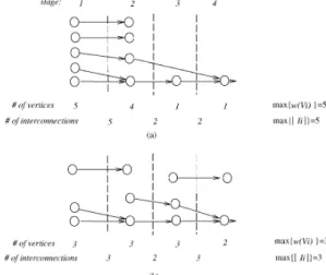
Unlike the traditional logic devices, the execution order of nodes in a DRD must follow their precedence (temporal) constraints. For example, a node in a combinational circuit must be executed no later than its outputs. It implies that a cut in a DRFPGA partitioning should be a uni-directional cut. Therefore, it is necessary to ensure the correct execution order of nodes. As an example, Figure 2 shows part of a design that has been partitioned into four memory planes in a DRD. Assume that a vertex requires a CLB and an interconnection requires an MR. Thus, the partitioning shown in Figure 2(a) needs five CLBs (# of vertices in the figure, max{w(Vi)}) and five MRs (# of interconnections in the figure, max{|Ii|}) while that shown in Figure 2(b) uses only three CLBs and three MRs.
Therefore, the partitioning shown in Figure 2(b) is desirable.
Figure 2: Precedence-constrained (temporal) partitioning.
Due to the precedence (temporal) constraints, all stages of the physical design for DRDs must consider the execution order and minimize the reconfiguration costs (reconfiguration time, reconfiguration power, etc.) as well
as the traditional costs (delay, area, etc). We describe the following physical design problems with the precedence (temporal) constraints as follows:
Temporal floorplanning: Given a set of circuit modules with precedence constraints among the modules, each with a fixed area, assign the modules into a chip so that a cost metric (area, wirelength, reconfiguration power, etc) is minimized.
Temporal placement: Given a set of circuit nodes with precedence constraints and a target DRD, place the nodes into the DRD so that a cost metric (total wirelength, reconfiguration power, etc) is minimized.
There is not much work on DRD placement, floorplanning, and routing. We formulated the temporal placement problem in [3] and presented a heuristic for handling the problem. Bazargan et. al. recently formulated a floorplanning problem for reconfigurable computing [4].
1.2 Integr ation of Functional Units
A reconfigurable system typically integrates a versatile set of functional units (e.g., multimedia units [subproject #1], communication units [subproject #2], microprocessors, embedded memory, and other general-purpose function units [subproject #6]). (Currently, designs with tens of millions transistors have been in production.) On one hand, designs with such high complexity need to handle large-scale circuits. On the other hand, the highly competitive IC market requires faster design convergence, faster incremental design turnaround, and better silicon area utilization. Efficient and effective hierarchical design methodology and tools capable of optimizing large-scale circuits are essential for such large designs.
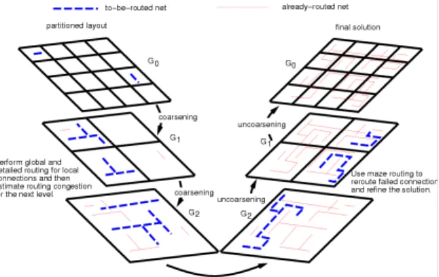
Figure 3. The multilevel framework for routing.
Traditional physical design algorithms do not scale well as the design size, complexity, and constraints increase, mainly due to their inefficiency, inflexibility in handling non-hierarchical data structures. We study in this project a multilevel framework to handle the physical design problems for large-scale circuits. A multilevel framework typically consists of two stages (see Figure 3), coarsening followed by uncoarseninging. The coarsening stage iteratively groups a set of circuit components (nodes, modules, nets, etc) based on a cost metric. The uncoarsening stage iteratively ungroups a set of the previously clustered circuit components and then refines the design solution. Based on the multilevel framework, we propose to study the partitioning, floorplanning, placement, and routing problems to handle large-scale circuits. The multilevel framework for partitioning has been studied extensively in the literature (e.g., [5], Chaco [6], Metis [7], ML [8]) while there is not much work on multilevel circuit placement [9] and multilevel routing [10]. The work [9] is based on the interior-point and the multipole methods, which obtains only slightly better wirelength but uses much longer running time than GORDIAN [11], a traditional placer. The work [10] considers only routability, which is not sufficient for modern performance-oriented circuit designs. Therefore, it is desirable to develop efficient and effective performance-driven multilevel frameworks for floorplanning, placement, and routing to handle large-scale circuits.
1.3 Optimization of Electr ical Effects
Voltage drop is mainly due to the resistance of the on-chip power
distribution network. When a large current flows through, un -acceptable
voltage drop may happen. The voltage drop may cause timing uncertainty
and slew rate slow -down, hence affecting performance and increasing power
consumption.
In the past, l ow resistance in a power system and relatively low
current levels made voltage drop a second -order effect that could safely
be ignored. In deep sub -micron (DSM) technology, the reduced power supply
voltage, increased current density, and thinner wires used in designs are
causing an increase in the number of failures in the power distribution
networks.
As a result, design of power distribution networks becomes an
important task. With lower supply voltages yielding smaller noise margins,
voltage drop is a fir st-order effect and can no longer be ignored during
the design process.
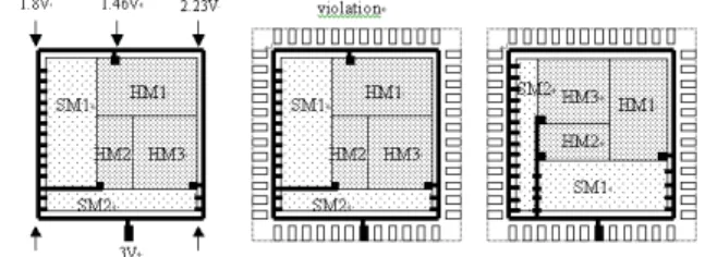
We show the voltage drops by power distribution network. Figure
4(a) depicts the different voltage drops at neighboring nodes. Suppose
that the minimum voltage required is Vmin. Fi gure 4(b) shows the voltage
drop of HM1 is greater than Vmin, and we try to find a signal -integrity
(SI) driven floorplanning under all voltage drops are satisfied, as shown
in Figure 4(c).
Figure 4: (a) The different voltage drops at n eighboring nodes; (b) The
voltage drop of HM1 is greater than Vmin; (c) An SI -driven floorplanning
is used to solve the voltage drop problem.
四
﹑
研究方法
We discuss the underlying techniques, approaches, and solutions for
handling the proposed problems.
1. Physical Design for Reconfigurable Circuits
1.1. Problem Formulation
In the reconfigurable architecture, a task v is loaded into the device
for a period of time for execution. Let V={v
1, v
2,..., v
m} be a set of m
tasks whose widths, heights, and durations are denoted by W
i, H
i, and T
i,
m i≤
≤
1
. Let (x
i, y
i) ((x'
i, y'
i)) denote the coordinate of the bottom-left
(top-right) corner of a task v
iand,
1≤i≤m, on the chip. We use t
i(t'
i)
to represent the starting (ending) time of v
i,
1≤i≤m, scheduled in the
reconfigurable device.
To guarantee the correctness of the functions in the reconfigurable
architecture, we must satisfy temporal precedence requirements, which
describe the temporal ordering among tasks. We refer to the temporal
precedence
requirements
as
precedence
constraints.
Let
} , , 1 | ) {(v, i j mi j D j v i ≤ ≤ ≠
=
denote the precedence constraints for the tasks v
iand
v
j.
The precedence constraints should not be violated during
1.2. Techniques and Approaches
We solve the 3-dimensional floorplanning/placement problems of the
general reconfigurable architecture by using a novel topological
floorplan
representation,
called
3D-subTCG
(3-Dimensional
sub-Transitive Closure Graph). To our best knowledge, this is the first
work that uses a topological representation to handle the 3-dimensional
placement problem of a dynamically reconfigurable device.
Transitive closure graphs were previously proposed to handle
classical 2D floorplanning/placement problems [12]. The main challenge
to solve the 3D floorplanning problems is that there exists additional
temporal precedence constraints, for which some tasks must be executed
before other tasks start. We use the 3D-subTCG which consists of three
transitive closure graphs to model the temporal as well as the spatial
relations between tasks/modules. We derive the feasibility conditions for
the temporal precedence and the spatial constraints induced by the
execution of the DRFPGAs. Because the geometric relationship is
transparent to the 3D-subTCG and its induced operations, we can easily
detect any violation of temporal precedence and spatial constraints in
the 3D-subTCG. Therefore, we can guarantee a feasible solution without
resorting to time-consuming post-processing to remove infeasible ones.
We also derive important properties of the 3D-subTCG to reduce the
solution space and shorten the running time for 3D (temporal)
foorplanning/placement.
2. Integration of Functional Units
2.1. Problem Formulation
2.1.1. Large-scale Cell Placement
Let B={b
1, b
2,..., b
m} be a set of m rectangular modules whose width,
height, and area are denoted by W
i, H
i, and A
i,
1≤i≤m. Let (x
i, y
i) denote
coordinate of the bottom-left corner of module bi,
1≤i≤m, on a chip. A
placement P with the alignment and the performance constraints is an
assignment of (x
i, y
i) for each bi,
1≤i≤m, such that no two modules overlap
and
the
given
constraints
are satisfied.
The
goal
of
floorplanning/placement is to optimize a predefined cost metric, such as
the area (the minimum bounding rectangle of P)), induced by the assignment
of b
i's on the chip.
2.1.2. Large-scale Net Routing
Routing is the process of interconnecting nets of the same signal.
Typically, the objectives are area and timing optimization subject to a
set of constraints such as the placement constraint, the number of
available routing layers, design rules, crosstalk, etc. Given a netlist
N = {N
1, N
2, … , N
n} and a chip structure with dimension and layer
information, find a route for each net Ni such that the total wirelength
is minimized and a set of constraints such as the capacity constraint of
each region, timing, etc., are satisfied.
2.2. Techniques and Approaches
2.2.1. Large-scale Cell Placement
We handle the placement with the alignment and performance
constraints using the B*-tree representation. We first explore the
feasibility conditions with the alignment and performance constraints,
and then propose algorithms that can guarantee a feasible placement with
alignment and performance constraints during each operation. In
particular, our method is the first algorithm to achieve the theoretically
optimal O(n)-time complexity for evaluating a placement with the
alignment and performance constraints, where n is the number of blocks.
(Note that O(n) is the lower-bound complexity for packing n blocks.)
Experimental results based on the MCNC benchmark with the constraints show
that our method significantly outperforms the previous work; for example,
our method achieved an average smaller area than that reported by [13].
2.2.2. Large-scale Net Routing
Our multilevel routing algorithm is inspired by the work [14].
Nevertheless, our framework is significantly different from [14]. During
the coarsening stage of the work [14], instead of routing or plan ning wires,
they only estimate routing resources by using a line -sweep algorithm and
then recursively coarsen to the last level k. Since their coarsening stage
does not perform real routing, it is hard to retrieve the routing
information at the higher level, which may make real routing resource
estimation inaccurate. At the last level k, they apply a multicommodity
flow algorithm to obtain an initial routing and avoid the net ordering
problem. However, a router may encounter higher congestion when
uncoarsening expands local nets. A bad initial routing at the higher level
needs more time to re-route at the lower level because of lacking local
routing information. This problem is also with the hierarchical approach.
Our router tends to route shorter nets first since we route local nets
at each level of coarsening. It is obvious that the local nets at the lower
level (say, level 0) are usually shorter than those at a higher level (say,
level k). Naturally, a shorter net enjoys less freedom while searching
for a path to route it. This fact holds even during rip-up and re-route.
Thus, this observation implicitly suggests that a shorter net has a higher
priority than a longer net as far as routability is concerned. Kastner,
Bozorgzadeh, and Sarrafzadeh in [15] also suggest this conclusion.
Thought this net ordering scheme may not be the optimal solution for some
routing problems (for example, when timing is considered, routing the most
critical net first often leads to better timing performance), it is still
a reasonable alternative.
2.3. Optimization of Electrical Effect
2.3.1. Problem Formulation
We focus on the analysis of the P/G distribution network at
post-floorplanning. Given power pads and cell library information, we
determine the P/G distribution network such that its voltage drop is
minimized.
n
Voltage Drop Constraints
To ensure the correct and reliable logic operation, we should restrict
the voltage drop from the P/G pads to the absorb pins in a network. The
voltage associated with an absorb pin is denoted by Vi. Therefore, for
every absorb pin i, the corresponding voltage Vi has to satisfy the
following constraints:
max
V
Vj≤
for power networks,
max
V
Vi≥
for ground networks,
where Vmin (Vmax) is the minimum (maximum) voltage required at the
injection point of a power (ground) network. They are given constants
based on the technology.
n
Minimum Width Constraints
For different process rules, we should restrict the metal wire width
in the P/G network. Given a set of nodes of a P/G network N = {1 ,… ,n},
each branch connects two nodes: i
1and i
2with current flowing from i1 to
i2. Let l
iand w
ibe the length and width of branch i, respectively. Let
ρbe the sheet resistivity. Then the resistance r
iof branch i is
i i i i i i
w
l
I
V
V
r
= 1− 2 =ρ
The widths of P/G segments are technologically limited to the minimum
width allowed in the layer where the segment lies. Thus, we have
, min , 2 1 min , i i i i i i w V V I l w ≥ − =ρ
where w
i,minis a given constant.
2.3.2. Techniques and Approaches
We address the analysis of the power distribution networks at the
block-level floorplanning stage. Most previous works for the analysis of
power distribution networks target for transistor or cell -level designs,
and perform at the routing stage. In this thesis, we address the design
of power distribution networks at the block -level floorplanning stage to
facilitate design convergence. Based on an equivalent current source
model for macro blocks, we first present a planning algorithm for power
distribution network to shorten the current paths from power supply pad
to local power supply wiring, and then integrate the power supply planning
algorithm into a floorplanner. Experimental results show that our
approach can eliminate all errors due to voltage drop.
五﹑
成果 (Publications)
1. Y.-W. Chang and S.-P. Lin, "MR: A New Framework for Multilevel Full-Chip Routing," accepted and to appear in IEEE Trans. Computer-Aided Design, 2003.
2. M.-C. Wu and Y.-W. Chang, ``Placement with Alignment and Performance Constraints," submitted to ICCAD 2003. 3. P.-H. Yuh, C.-L. Yang, Y.-W. Chang, and H.-L. Chen, ``A Graph-Based Formulation for Temporal Floorplanning," submitted
to ICCAD 2003.
4. S.-W. Wu and Y.-W. Chang, ``Fast Power/Ground Network Synthesis for Signal Integrity-Driven Floorplanning," submitted to ICCAD 2003.
六
﹑
參考文獻
[1] S. Trimberger, ``A Time-Multiplexed FPGA,'' in IEEE Workshop on FPGAs for Custom computing Machines, 1997,pp. 22-28. [2] Xilinx, “The Programmable Logic Data Book,” 1996.
[3] G.-M. Wu, J.-M. Lin, and Y.-W. Chang, ``Generic ILP-based approaches for time-multiplexed FPGA partitioning," in IEEE Trans. Computer-Aided Design, Vol. 20, No. 10, pp. 1266-1274, October 2001.
[4] E. Bazargan, R. Kastner, and M. Sarrafzadeh, “3-D floorplanning: Simulated annealing and greedy placement methods for reconfigurable computing systems,” IEEE FCCM, 2001.
[5] J. Cong and M. L. Smith, “A parallel bottom-up clustering algorithm with applications to circuit partitioning in VLSI design,” Proc. of DAC, pp. 755-760, 1993.
[6] G. Karypis and V. Kumar, “Multilevel graph partitioning scheme,” in P. Banerjee and P. Boca, Eds., Proc. of 1995 Int. Conf. Parallel Processing, Vol. 3, pp. 113-122, 1995.
[7] J. M. Kleinhans, G. Sigl, F. M. Johannes, and K. J. Antreich, “GORDIAN: VLSI placement by quadratic programming and slicing optimization,” IEEE Trans. Computer-Aided Design, vol. 10, no. 3, pp. 356-365, 1991.
[8] C. J. Alpert, J.-H. Huang, and A. B. Kahng, “Multilevel circuit partitioning,” IEEE Trans. Computer-Aided Design, vol. 17, no. 8, pp. 655-667, August 1998.
[9] T. F. Chan, J. Cong, T. Kong, and J. R. Shinner, “Multilevel optimization for large-scale circuit placement,” Proc. of ICCAD, pp. 171-176, Nov. 2000.
[10]J. Cong, J. Fang, and Y. Zhang, “Multilevel approach to full-chip gridless routing,” Proc. of ICCAD, pp. 396-403, Nov. 2001.
[11]G. Sigl, K. Doll, and F. M. Johannes, “Analytical placement: A linear or a quadratic objective function?” Proc. of DAC, pp. 427-432, 1991. [12]J.-M. Lin and Y.-W. Chang, “TCG: A transitive closure graph based representation for non-slicing floorplans,” Proc. of DAC, pp. 764-769, Las
Vegas, NV, June 2001.
[13]X. Tang and D.F. Wong, "Floorplanning with alignment and performance constraints," Proc. of DAC, pp. 848-853, 2002. [14]J. Cong, J. Fang and Y. Zhang, ``Multilevel approach to full-chip gridless routing,'' Proc. of ICCAD, pp. 396-403, Nov. 2001. [15]R. Kastner, E. Bozorgzadeh and M. Sarrafzadeh, ``Predictable routing,'' Proc. of ICCAD, pp. 110-114, Nov. 2000.