High Light-Extraction GaN-Based Vertical LEDs
With Double Diffuse Surfaces
Ya-Ju Lee, Hao-Chung Kuo, Senior Member, IEEE, Tien-Chang Lu, and Shing-Chung Wang, Senior Member, IEEE
Abstract—High light-extraction (external quantum efficiency 40%) 465-nm GaN-based vertical light-emitting diodes (LEDs) employing double diffuse surfaces were fabricated. This novel LED structure includes one top transmitted diffuse surface and another diffuse omnidirectional reflector (ODR) on the bottom of a LED chip. The diffusive ODR consists of a roughened p-type GaN layer, an indium–tin–oxide (ITO) low refractive index layer, and an Al layer. The surface of the p-type GaN-layer was nat-urally roughened while decreasing the growth temperature to 800 C. After flip-bonding onto a Si substrate by AuSn eutectic metal and laser lift-off processes to remove the sapphire substrate, an anisotropic etching by dilute potassium hydroxide (KOH) was employed on the -face n-GaN layer to obtain transmitted diffuse surfaces with hexagonal-cone morphology. The double diffused surfaces LEDs show an enhancement of 56% and 236% in light output power compared to single side diffused surface and conventional LEDs, respectively. The devices also show a low leakage current in the order of magnitude of 10 8 A at 5 V and a calculated external quantum efficiency of about 40%. The high scattering efficiency of double diffused surfaces could be responsible for the enhancement in the device light output power.
Index Terms—Double diffuse surfaces, GaN, light-emitting diodes (LEDs), light-extraction efficiency.
I. INTRODUCTION
W
IDE BANDGAP light-emitting diodes (LEDs), that are III-Nitride, ranging from ultraviolet to the short-wave-length part of the visible spectrum have been intensely devel-oped in the past ten years [1], [2]. Recently, as the brightness of GaN-based LEDs has increased, applications such as traffic signals, backlight for cell phone, and short-haul communica-tions have become possible [3]. However, as for the replace-ment of conventional fluorescent lighting source with solid-state lighting, it still needs a great effort for improving the light-extraction efficiency as well as internal quantum efficiency of LEDs. Considering the large difference of the refractive index between GaN (n 2.5) and air, the critical angle for light ex-traction is only about 23 , i.e., approximately 4% of light fromManuscript received March 7, 2006; revised August 8, 2006. This work was supported in part by the National Science Council, Taiwan, R.O.C., under Con-tracts NSC 94-2120-M009-007 and NSC 94-2752-E009-007-PAE.
Y. J. Lee is with the Department of Photonic and Institute of Electro-Optical Engineering, National Chiao Tung University, Hsinchu 300, Taiwan, R.O.C., and also with the R&D Division, Epistar Company, Ltd., Hsinchu 300, Taiwan, R.O.C. (e-mail: [email protected]).
H. C. Kuo, T. C. Lu, and S. C. Wang are with the Department of Pho-tonic and Institute of Electro-Optical Engineering, National Chiao Tung University, Hsinchu 300, Taiwan, R.O.C. (e-mail: [email protected]; [email protected]; [email protected])
Color versions of Figs. 1, 2, and 5–7 are available online at http://ieeexplore. ieee.org.
Digital Object Identifier 10.1109/JQE.2006.883468
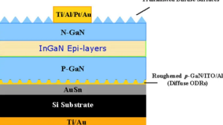
Fig. 1. Schematic cross section of a LED with double diffuse surfaces.
the active region can escape per surface. The light outside the escape cone is guided between sapphire substrate and the sur-rounding air, and then reabsorbed by active layers or electrodes. Therefore, there is much room for improving the light extrac-tion efficiency. Many approaches have been proposed to ob-tain high light-extraction efficiency including shaping of LEDs [4], [5], patterned sapphire substrates [6], roughening of the top LED surface [7], and introducing highly reflective omnidi-rectional reflectors (ODRs) [8]. Recently, Kim et al. proposes a novel structure using diffuse ODRs, enhancing the reflected power by two orders of magnitude for a roughened reflector surface compared with a planar surface [9]. According to their investigation, guided light is reflected diffusively by the rough-ened reflector, thus adding the light-extraction efficiency. In this work, we present a LED structure adopting double diffused-sur-faces—one top transmitted diffuse surface and another diffuse ODR surface on the bottom of a LED chip. According to this design, guided light scattered by bottom diffuse ODRs can be again scattered to angles inside the escape cone by top diffuse transmittance surfaces to achieve a high light external efficiency.
II. DEVICEFABRICATION
A schematic cross section image of a GaN-based LED with double diffuse surfaces is shown in Fig. 1. GaN-based LEDs used in this study were grown using a low-pressure metal-organic chemical vapor deposition (Aixtron 2600G) system onto the -face (0001) 2”-diamerter sapphire substrate. The LED layer-structure comprised a 30-nm-thick GaN nu-cleation layer grown at 520 C, a 2- m-thick undoped GaN layer grown at 1050 C, 2- m-thick Si-doped n-type GaN cladding layer grown at 1050 C, an un-intentionally doped active region of 465-nm with five periods InGaN–GaN multiple quantum wells (MQWs) grown at 700 C, and a 0.4- m-thick Mg-doped p-type GaN cap-layer. Two different p-type GaN
cap layers were used in this study. Samples A and B were grown at 1050 C and 800 C, respectively. At such a low grown temperature of GaN layers (i.e., 800 C), large number of hexagonal pits can be seen on the top surface of the LED surface. In order to measure the change of surface roughness of p-type GaN surface caused by grown temperature, atomic force microscopy (AFM) measurements were performed in this report. After subsequent depositions of a 200-nm-thick indium-tin-oxide (ITO, n 1.7 at 465-nm) low-refractive-index layer and a 500-nm-thick Al mirror layer on top of LEDs, the p-side surface of sample A could be served as specular ODRs (flat type GaN–ITO–Al) [15] and that of sample B could be served as diffuse ODRs (roughened type GaN–ITO–Al) [9]. Thick Au was deposited on both samples followed by Sn evaporation in a thermal evaporator. The wafer was then flipped and bonded to an Au-coated Si submount at a temperature of 350 C, resulting in an alloy of Au and Sn to form adhesion between the LED wafers and Si submounts. A KrF excimer laser at a wavelength of 248 nm with a pulsewidth of 25 ns was then used to remove the sapphire substrate [14]. The laser with a beam size of 1.2 mm 1.2 mm was incident from the backside of the sapphire substrate onto the sapphire–GaN interface to decompose GaN into Ga and N . In this process, the beam size of KrF laser was larger than that of the size of the LEDs. Therefore, the laser irradiation on the interface of sapphire and GaN was uniform. After laser lift-off process, the remaining GaN epitaxial film on the Si submount displayed a -face (000–1) surface. The remaining Ga droplets on the transferred GaN surface were removed by etching in a HCl solution. Next, the transferred GaN was thinned until the Si-doped GaN was exposed. An n-contact composed of Ti–Al–Pt–Au was formed on the exposed -face n-GaN and p-contact composed of Ti–Au was deposited on the Si-submount. Finally, in order to roughen the top of surface, dilute potassium hydroxide (KOH) was used as etching solution at 80 C. After wet etching, hexagonal cones can be observed on the -face n-GaN surface. The conventional LEDs with the same emitting wavelength as above two samples were also used as a reference to evaluate the optical and electrical properties of double diffused surfaces LEDs, where the p-type GaN cap layer of conventional LEDs was grown at 1050 C. The as-grown LED epitaxial layers were partially etched until the n-type GaN layers were exposed. Ni-Au transparent contact layers were subsequently evaporated onto the p-GaN cap layers to serve as the transparent contact layers (TCLs). A thick Au layer was then deposited onto part of the TCL to serve as the p-electrodes. Ti–Al–Pt–Au contacts were deposited onto the exposed n-GaN layers to serve as the n-electrodes. All LEDs were fabricated with the size of 350 350 m . The typical current–voltage ( – ) measurements were performed using a high current measure unit (KEITHLEY 240). The light output power of the LEDs was measured on TO-can without epoxy resin and used an integrated sphere with a calibrated power meter.
III. RESULTS ANDDISCUSSION
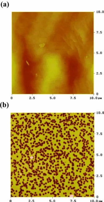
Fig. 2 shows AFM images of p-type GaN surface grown at (a) 1050 C and (b) 800 C. With the variation of grown temperature, the root-mean-square (rms) roughness of p-type
Fig. 2. AFM images of p-type GaN surface grown at (a) 1050 C and (b) 800 C. The rms roughness is (a) 2.3 and (b) 129.3 nm.
GaN increases from (a) 2.3 to (b) 129.3 nm, respectively. According to Fig. 2 (b), hexagonal V-shape pits distributed randomly and the surface density was estimated to be about 1.28 10 /cm . Fig. 3(a) and (b) shows the cross-sectional transmission electron microscope (TEM) images of sample A and sample B, respectively. In Fig. 3(a), the top surface of p-type GaN was quite flat, as can be seen in conventional LEDs; however, lots of hexagonal V-shape pits was observed on p-type GaN surface of sample B, as shown in Fig. 3(b). The diameter of hexagonal V-shape pits ranged from 200 to 400 nm, and the depth of pits was about 300 nm. Therefore, light emitted from LED active region could be scattered due to these randomly distributed hexagonal V-shape pits. Fig. 3(c) is an enlarged TEM image of one hexagonal V-shape pit. As can be seen in this figure, the hexagonal V-shape pit originated from threading dislocations and there is a thick dark band along the V-groove, being indicative of thickness variation. The formation of these
Fig. 3. Cross-sectional transmission electron microscope (TEM) images of (a) flat p-GaN surface (sample A) and (b) hexagonal V-shape roughened p-GaN surface (sample B). (c) is an enlarged TEM image of one hexagonal V-shape pit.
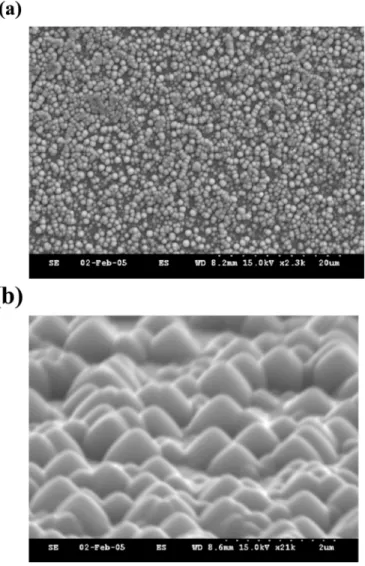
hexagonal V-shape pits could be attributed to the fact that Ga atoms might not have enough energy to migrate to proper sites. Thus, lateral growth rate of GaN will become smaller [10]–[13]. Fig. 4(a) shows the top-view scanning electron micrograph (SEM) image of -face n-GaN surface after KOH etching for 3 min. Shown in Fig. 4(b) was SEM image taken at an angle of 70 degrees from the perpendicular direction of the etched surface. According to this figure, the base and height of hexagonal cones are both about 400–600 nm. It should be noted that n-GaN surfaces of both sample A and B exhibit the same surface morphology since they were etched by KOH solution at the same time. Therefore, -face n-GaN surfaces with hexagonal cones features were quite suitable for serving as transmitted diffuse surfaces and an excellent transmitted ca-pability of this roughened morphology had been demonstrated [7]. Fig. 5(a) shows the light output power ( – curve) of sample A, sample B and conventional LEDs. The sample B, the LED with double diffuse surfaces, and sample A, the LED with flat ODRs, produced much higher light output as compared with that of conventional LEDs under all our measurement condition. For instance, the light output powers at 20 mA of sample A, sample B, and conventional LEDs are 13.6, 21.3, and 9 mW, respectively. Therefore, the light output at 20 mA of the sample B increases by 236% as compared with that of conventional LED and increases by 56% as compared with that of sample A. The calculated external quantum efficiency of our proposal LEDs with double diffuse surfaces is about 40% at
Fig. 4. SEM images of the N-face GaN etch morphology after an etch time of 3 min by KOH, 80 C. (a) Top-view and (b) is taken at an angle of 70 degrees from the perpendicular to the etched surface.
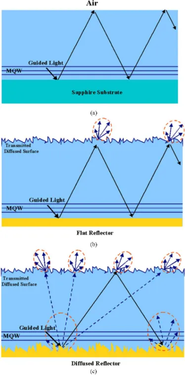
20 mA ( nm), which could compete with structures of state of the art [16]. Fig. 5(b) shows light output patterns of sample A, sample B and conventional LED at 20 mA. It is clear from the results that the EL intensities of sample B were larger than those of sample A and conventional LEDs. According to this figure, view angles (half-center brightness or 50% of the full luminosity) of sample A and sample B are almost the same, i.e., 120 ; however, the overall integrated area of EL intensities of sample B is still larger than that of sample A. Besides, al-though view angles of conventional LEDs is larger than that of sample A and sample B, i.e., 140 , due to the existing of trans-parent sapphire substrate; the enhancement of EL intensity by adopting double diffuse surfaces scheme is more remarkable, as compared that with conventional LEDs. The improvement in emitted light extraction efficiency is considered as a conse-quence of high light scattering efficiency by employing double diffuse surfaces. To understand the light-output enhancement of the LEDs made with double diffuse surfaces, the propagation of light emitted is schematically shown in Fig. 6. Fig. 6(a) shows a simple optical ray trace diagram of a conventional LED. In this case, the guided light emitting with an angle larger
Fig. 5. (a) Output power of sample A, sample B, and conventional LEDs mea-sured by an integral-sphere as a function of a forward dc current. (b) Light output patterns of sample A, sample B, and conventional LEDs.
than the critical angle would be trapped between sapphire sub-strate and the surrounding air, and finally be vanished through absorption of active layers or electrodes. Fig. 6(b) shows the case of sample A by employing transmitted diffuse surfaces on top and flat ODRs on bottom of LED chips. According to this figure, guided light could be extracted outside LED chips by scatterings at transmitted diffuse surfaces; therefore in this case, the escaping probability of photons is larger as compared with that of conventional LEDs. However, guided light needs multiple reflections by the bottom diffuse omnidirectional surfaces before being scattered again by the top transmitted diffuse surfaces. When we replace flat ODRs with diffuse or roughened surfaces, as shown in Fig. 6(c), the situation is quite different. In Fig. 6(c), guided light emitted towards to diffuse ODRs is scattered. The scattering light will be scattered again by top transmitted diffuse surfaces, adding total probability for photons to escape outside LED chips. Therefore, higher guided light scattering efficiency was achieved by adopting double diffuse surfaces scheme, as shown in Fig. 6(c). It’s the reason why sample B demonstrated the best light output compared to sample A and conventional LEDs in all our measurement conditions.
As for the electrical characteristics, all LEDs demonstrate forward voltages of 3.2 V at 20 mA, which is a typical and acceptable value while comparing to other devices with same chip size (350 350 m ). Another important electrical prop-erty needed to certify is the reverse leakage current, since the
Fig. 6. Simple optical ray diagrams of (a) conventional LEDs, (b) sample A with top transmitted diffuse surfaces and bottom flat ODRs and (c) sample B with top transmitted diffuse surfaces and bottom diffuse ODRs.
roughened surfaces could easily induce leakage paths. Espe-cially at the procedure of fabricating diffuse ODRs (roughened p-type GaN–ITO–Al), leakage paths may penetrate through V-shape pits to MQWs, degrading LED performances. There-fore, in order to avoid electrical short circuit, specific control of epitaxial condition while growing hexagonal V-shape pits is important. Fig. 7 shows the reverse voltage versus current characteristics of sample A, sample B, and conventional LEDs (each curve represents 10 LED devices average results). It was found that the leakage currents of all LEDs at 5 V were in the order of magnitude of 10 A, indicating the roughening
Fig. 7. Leakage current as function of reverse voltage for sample A, sample B, and conventional LEDs.
processes, no matter by epitaxial growth (hexagonal pits) or chemical wet etching (hexagonal cones), did not adversely affect the LED performance.
IV. CONCLUSION
In conclusion, high light-extraction 465-nm GaN-based ver-tical LEDs were successfully fabricated with double diffuse sur-faces scheme. One surface was a diffusive ODR consisted of an epitaxially roughened p-type GaN layer, an ITO layer, and an Al layer, and another was a wet-chemical etched -face n-GaN transmitted diffuse surface. The external quantum effi-ciency was calculated to be about 40%. The high performance LED was achieved mainly due to the strong guided-light scat-tering efficiency while employing double diffuse surfaces. The forward voltages was 3.2 V at 20 mA and the leakage cur-rents at 5 V was in the order of magnitude of 10 A, in-dicating the roughening processes, did not adversely affect the LED performance.
ACKNOWLEDGMENT
The authors would like to thank Prof. K. M. Lau of Hong Kong University of Science and Technology and Prof. Pilkuhn of National Chiao Tung University for useful discussion.
REFERENCES
[1] E. Fred Schubert, Light-Emitting Diodes. Cambridge, U.K.: Cam-bridge Univ. Press.
[2] A. Zukauskas, M. S. Shur, and R. Gaska, Introduction to Solid-State
Light. New York: Wiley.
[3] M. Koike, N. Shibata, H. Kato, and Y. Takahashi, “Development of high efficiency GaN-based multiquantum-well light-emitting diodes and their applications,” IEEE J. Sel. Topics Quantum Electron., vol. 8, no. 2, pp. 271–277, Mar./Apr. 2002.
[4] M. R. Krames, M. Ochiai-Holcomb, G. E. Höfler, C. Carter-Coman, E. I. Chen, I.-H. Tan, P. Grillot, N. F. Gardner, H. F. Gardner, H. C. Chui, J.-W. Huang, S. A. Stockman, F. A. Kish, and M. G. Craford, “High-power truncated-inverted-pyramid (Al Ga ) In P/GaP light-emitting diodes exhibiting> 50% external quantum efficiency,”
Appl. Phys. Lett., vol. 75, pp. 2365–2367, 1999.
[5] Y. J. Lee, H. C. Tseng, H. C. Kuo, S. C. Wang, C. W. Chang, T. C. Hsu, Y. L. Yang, M. H. Hsieh, M. J. Jou, and B. J. Lee, “Improve-ment in Light-Output Efficiency of AlGaInP LEDs Fabricated on Stripe Patterned Epitaxy,” IEEE Photon. Technol. Lett., vol. 17, no. 12, pp. 2532–2534, Dec. 2005.
[6] Y. J. Lee, J. M. Hwang, T. C. Hsu, M. H. Hsieh, M. J. Jou, B. J. Lee, T. C. Lu, H. C. Kuo, and S. C. Wang, “Enhancing output power of GaN-based LEDs grown on chemical wet etching patterned sapphire substrate,” IEEE Photon. Technol. Lett., vol. 18, no. 10, pp. 1152–1154, Oct. 2006.
[7] T. Fujii, Y. Gao, R. Sharma, E. L. Hu, S. P. DenBaars, and S. Naka-mura, “Increase in the extraction efficiency of GaN-based light-emit-ting diodes via surface roughening,” Appl. Phys. Lett., vol. 84, pp. 855–855, 2004.
[8] T. Gessmann, H. Luo, J.-Q. Xi, K. P. Streubel, and E. F. Schubert, “Light-emitting diodes with integrated omnidirectionally reflective contacts,” Proc. SPIE, vol. 5366, pp. 53–61, 2004.
[9] J. K. Kim, H. Luo, Y. Xi, J. M. Shah, T. Gessmann, and E. F. Schubert, “Light extraction in GaInN light-emitting diodes using diffuse omni-directional reflectors,” J. Electrochem. Soc., vol. 153, pp. G105–G107, 2006.
[10] D. I. Florescu, S. M. Ting, J. C. Ramer, D. S. Lee, V. N. Merai, A. Parkeh, D. Lu, E. A. Armour, and L. Chernyak, “Investigation of V-de-fects and embedded inclusions in InGaN/GaN multiple quantum wells grown by metalorganic chemical vapor deposition on (0001) sapphire,”
Appl. Phys. Lett., vol. 83, pp. 33–35, 2003.
[11] S. M. Ting, J. C. Ramer, D. I. Florescu, V. N. Merai, B. E. Albert, A. Parkeh, D. S. Lee, D. Lu, D. V. Christini, L. Liu, and E. A. Armour, “Morphological evolution of InGaN/GaN quantum-well heterostruc-tures grown by metalorganic chemical vapor deposition,” J. Appl.
Phys., vol. 94, pp. 1461–1467, 2003.
[12] Y. K. Su, S. J. Chang, S. C. Wei, S. M. Chen, and W. L. Li, “ESD En-gineering of Nitride-Based LEDs,” IEEE Trans. Device Mater. Reliab., vol. 5, no. 2, pp. 277–281, Jun. 2005.
[13] S. J. Chang, L. W. Wu, Y. K. Su, Y. P. Hsu, W. C. Lai, J. M. Tsai, J. K. Sheu, and C. T. Lee, “Nitride-based LEDs with 800 C grown p-AlInGaN-GaN double-cap layers,” IEEE Photon. Technol. Lett., vol. 6, no. 6, pp. 1447–1449, Jun. 2004.
[14] J. T. Chu, T. C. Lu, H. H. Yao, C. C. Kao, W. D. Liang, J. Y. Tsai, H. C. Kuo, and S. C. Wang, “Laser lift-off fabrication of blue-violet GaN-based vertical cavity surface emitting lasers optically pumped at room temperature,” Jpn. J. Appl. Phys., vol. V45, no. 4A, pp. 2556–2560, 2006.
[15] Th. Gessmann, Y.-L. Li, E. F. Schubert, J. W. Graff, and J. K. Sheu, “GaInN light-emitting diodes with omni directional reflectors,” Proc.
SPIE, vol. 4996, pp. 139–144, 2003.
[16] M. G. Craford, “LEDs for solid state lighting and other emerging ap-plications: Status, trends, and challenges,” Proc. SPIE, vol. 5941, pp. 594101-1–594101-10, 2005.
Ya-Ju Lee received the B.S. degree in physics from
National Central University, Taiwan, R.O.C., in 2000, and the M.S. degree from the Institute of Electro-Optical Engineering, National Chiao Tung Univer-sity, Taiwan, R.O.C., in 2002. He is currently working toward the Ph.D. degree in the Department of Pho-tonics and Institute of Electro-Optical Engineering, National Chiao Tung University, Taiwan, R.O.C.
He is also a Research Engineer in the R&D Depart-ment, Epistar Corporation, Hsinchu, Taiwan, R.O.C.
Hao-Chung Kuo (M’98–SM’06) received the B.S.
degree in physics from National Taiwan University, Taiwan, R.O.C., the M.S. degree in electrical and computer engineering from Rutgers University, New Brunswick, NJ, in 1995, and the Ph.D. degree from Electrical and Computer Engineering Department, University of Illinois at Urbana Champaign, in 1999. He has an extensive professional career both in research and industrial research institutions that in-cludes: Research Consultant in Lucent Technologies, Bell Laboratories (1993–1995); a Senior Research Engineer at Filtronic Solid State (1999–2000); and a Member of Technical Staff in Fiber-Optics Division at Agilent Technologies (2000–2001) and LuxNet Corporation (2001–2002). Since October 2002, he has been with the National Chiao Tung University as a Faculty Member of the Institute of Electro-Optical Engineering. His current research interests include semiconductor lasers,
VCSELs, blue and UV LED lasers, quantum-confined optoelectronic struc-tures, optoelectronic materials, and high-speed semiconductor devices. He has authored and coauthored 80 internal journal papers and 4 granted patents.
Dr. Kuo is member of SPIE and MRS.
Tien-Chang Lu received the B.S. degree in
elec-trical engineering from National Taiwan University, Taiwan, R.O.C., in 1995, the M.S. degree in electrical engineering from the University of Southern Los Angeles, in 1998, and the Ph.D. degree in electrical engineering and computer science from National Chiao Tung University, Taiwan, R.O.C., in 2004.
He joined the National Chiao Tung University as a faculty member of Department of Photonics in August 2005.
Shing-Chung Wang (M’79–SM’03) received the
B.S. degree from National Taiwan University, Taiwan, R.O.C., the M.S. degree from National Tohoku University, Sendai, Japan, and the Ph.D. degree from Stanford University, Stanford, CA, in 1971, all in electrical engineering.
He has an extensive professional career both in academic and industrial research institutions that includes: a faculty member at National Chiao Tung University (1965–1967); a Research Associate at Stanford University (1971–1974); a Senior Research Scientist at Xerox Corporation (1974–1985); and a Consulting Scientist at Lockheed-Martin Palo Alto Research Laboratories (1985–1995). In 1995, he rejoined National Chiao Tung University, Taiwan, R.O.C., as a faculty member of Institute of Electro-Optical Engineering. His current research interests include semiconductor lasers, VCSELs, blue and UV lasers, quantum-confined optoelectronic structures, optoelectronic materials, diode-pumped lasers, and semiconductor laser applications.
Prof. Wang is a Fellow of the Optical Society of America and a recipient of Outstanding Scholar Award from the Foundation for the Advancement of Outstanding Scholarship.