國 立 交 通 大 學
電 子 工 程 學 系 電 子 研 究 所
碩 士 論 文
具有鈷/鈦/鋁催化金屬和新穎自動聚焦閘極結
構之奈米碳管場發射元件之研究
Study on the Carbon-Nanotube Field Emission
Devices with the Co/Ti/Al Catalyst and Novel
Self-Focusing Gate Structure
研 究 生:陳 俠 威
指導教授:鄭 晃 忠 博士
中華民國 九十六 年 七 月
具有鈷/鈦/鋁催化金屬和新穎自動聚焦閘極結構
之奈米碳管場發射元件之研究
Study on the Carbon-Nanotube Field Emission
Devices with the Co/Ti/Al Catalyst and Novel
Self-Focusing Gate Structure
研 究 生:陳俠威 Student : Hsia-Wei Chen
指導教授:鄭晃忠 博士 Advisor : Dr. Huang-Chung Cheng
國 立 交 通 大 學
電子工程學系 電子研究所碩士班
碩士論文
A Thesis
Submitted to Department of Electronics Engineering & Institute of Electronics College of Electrical and Computer Engineering
National Chiao Tung University in Partial Fulfillment of the Requirements
for the Degree of Master In
Electronics Engineering 2007
具有鈷/鈦/鋁催化金屬和新穎自動聚焦閘
極結構之奈米碳管場發射元件之研究
研究生:陳俠威 指導教授:鄭晃忠 博士
國立交通大學電子工程學系
電子研究所碩士班
摘
要
本實驗室已經研究多層催化金屬在低溫下合成奈米碳管,其中以
鈷/鈦/鋁和鈷/鉻/鋁表現最好,然而在 550℃下,中間層鈦金屬的場
發射特性表現又明顯優於鉻,但是,尤其在更低溫 500℃下,它們的
特性並沒有在我們預期中的好,因此,本篇論文主要在解決奈米碳管
在 500℃下,有效率與最佳化的合成,最佳化的合成條件是利用乙烯、
氫氣和氮氣的流量控制達成的,經由電子顯微鏡、拉曼光譜以及場發
射特性的量測可以達到證實,我們甚至在 370℃的超低溫下利用熱化
學氣相沉積法合成出奈米碳管,未來如更降低此沈積溫度,將可以運
用在塑膠軟板上,當作量產化的生化感應晶片使用。
利用熱化學氣相沉積法合成出奈米碳管,多層催化金屬鈷/鈦/
鋁有相當高的成長速率,利用最佳化的成長條件與在不同的溫度下合
成奈米碳管,求得多層催化金屬的活化能,由實驗結果得知,多層催
化金屬的活化能為 0.89 電子伏特,相對的低於單層催化金屬的 1.54
電子伏特,活化能的降低是多層催化金屬能夠在低溫下成長出奈米碳
管的一個證據之一,利用原子力顯微鏡,可以證實金屬鋁為平均分散
奈米顆粒的效果,利用沒有中間層鈦的方式,間接證實鈦的功能是增
加鈦原子的析出,此三層金屬在低溫下合成奈米碳管缺一不可,由於
它們有各自的功能。
利用上述在低溫合成催化金屬的技巧,使用多層催化金屬,研發
出一種以奈米碳管為場發射源的自動聚焦閘極結構,這種三極結構的
閘極,可以有擷取出電子束的功能,同時,又可以擁有電子束聚焦的
功能,不像其他運用在場發上元件上的結構,需要多一層聚焦層,不
但增加成本,且複雜了製程;本發明只需要簡單的結構就可以達到聚
焦功能,對稱長條狀的閘極設計,是經由多次的模擬所得到最佳化的
設計,經過實驗結果與發光效果驗證它的可行性。在模擬中,傳統的
三極結構的亮點長達 622um,相反的,新穎自動聚焦閘極結構只有
232um,實際成品,也相差不遠;未來在大面積場發射螢幕上的運用,
由於此新穎的結構具有製程簡單以及成本便宜的優勢下,非常大有可
為。
Study on the Carbon Nanotubes Field
Emission Devices with the Co/Ti/Al Catalyst
and Novel Self-Focusing Gate Structure
Student : Hsia-Wei Chen Advisor : Dr. Huang-Chung Cheng
Department of Electronics Engineering &
Institute of Electronics
National Chiao Tung University
Abstract
In order to decrease the cost and improve the uniformity of CNT-FEDs, the CVDs process is necessary for the synthesis of CNTs on glass substrate at low temperatures below the softening point of glass (~550 ). In this thesis℃ , the thermal CVD was employed to synthesize CNTs at temperatures (lower than 500 ).℃ As a multilayer catalyst, Co/Ti/Al, has been successfully utilized to synthesize carbon nanotubes (CNTs) at 550 ℃ by thermal CVD previously. Its morphologies and field emission characteristics are not as good as we thought. Therefore, the objective of this thesis is optimizing and achieving an effective growth of CNTs using Co/Ti/Al catalyst at 500 ℃ or even lower temperatures to improve the characteristics of CNTs by controlling the flow rates of ethylene, hydrogen and nitrogen. According to the
10, 100, and 125 sccm, respectively. It is also found that nanotubes grown using this recipe at 500 ℃exhibited excellent field emission characteristics.
Co/Ti/Al is used to synthesize CNTs at atmospheric pressure by thermal CVD. The relative growth rates, calculated on the basis of the average lengths of nanotubes grown at different temperatures, are utilized to estimate an activation energy of 0.89 eV for the multilayer catalyst as compared with 1.54 eV for the single Co catalyst. Low activation energy is the indirect evidence for CNTs grown at low temperature. Such a low activation energy implies that the nucleation and growth of nanotubes could be effectively enhanced via the multilayer catalyst due to the well-distributed small catalytic nanoparticles by Al supporting layer and higher activity from Ti layer. A self-focusing gate structure is fabricated for the CNT devices with growth conditions is as the same as that mentioned above. The symmetric gate electrode can be employed to extract electrons; meanwhile, it can also act as a focus lens. According to the simulation results and luminescent images, this self-focusing gate structure has a well controllability on the trajectory of electrons emitted from CNTs, and therefore represents a smaller luminescent spot size than conventional structure; that is, it shows an excellent focusing effect. The novel gate structure which only adopts a simple fabrication process has the advantages of low-cost manufacturing and scalability, and is promising for the application in field emission diplays.
誌 謝
首先要感謝國立交通大學所有教導過我的老師,尤其是我的指導教授—鄭晃 忠老師,謝謝他在論文研究與為人處世方面的指導與鼓勵,才能使我順利的完成 碩士學位。 其次,感謝交通大學半導體中心和國家毫微米實驗室提供完善的實驗設備, 以及所有曾經幫助過我的技術員,黃月美小姐、徐秀鑾小姐、陳聯珠小姐、范秀 蘭小姐、葉雙得先生、胡進章先生。也感謝何惟梅小姐在行政方面的協助。 感謝這兩年與我相處的直屬學長,林高照,雖然你的話總是不多,但是我知 道你內心是熱情的(由你的衣服略知一二),因為你帶著我作實驗,我這兩年才 可以順利的畢業。感謝凱方與祐圻同學,不管是實驗上或生活上彼此的照應與幫 助;感謝春乾學長、瑞霖學長、逸哲學長和全平學長給我不吝嗇的指教;感謝學 眾學弟妹們的協助,尤其感謝政欽、建穎、君翰、型男和育瑛,你們實在太傑出、 太搞笑了,添加我生活中不少的樂趣。特別感謝大傳學長,因為你的聯誼讓我碩 士班的生活更多彩多姿,還讓我認識個性不錯的女孩。 最後感謝我的父親-陳遠興先生與我的母親-方世榮女仕,對我的教誨,一直 在身旁支持著我並給我無憂無慮的生活,感謝我的哥哥--俠鶴,你總是那麼關心 我;感謝我的好朋友,有你在我身邊度過每一道難關。 畢業是另一段旅程的開始,希望大家在未來都可以發揮所長,一路順風。Contents
ABSTRACT (in Chinese)...i
ABSTRACT (in English)………..………..……….……….iii
ACKNOWLEDGEMENTS……….……….……….v
CONTENTS……….……….vi
TABLE LISTS……….……….……….ix
FIGURE CAPTIONS………..………...………x
CHAPTER 1:Introduction
1.1 Overview of Vacuum Microelectronics………...11.1.1 History of Vacuum Microelectronics………...………...1
1.1.2 Theory Background…………...………..………. ....4
1.2 The Structure and Technology Trends for Field Emission Display………...9
1.2.1 Application of Vacuum Microelectronics………..………..…....9
1.2.2 Cold Cathode Structures and Materials for Field Emission Displays.…...11
1.2.2.A Spindt-Type Field Emitters………...……...………...12
1.2.2.B BSD Field Emitters……….…....………...14
1.2.2.C MIM Field Emitters………..…………..…….………...……...14
1.2.2.D SCE Field Emitters……….….………...…...15
1.3 The Promising Field Emission Technology – Carbon Nanotubes…………...17
1.3.1 The Synthesis Methods of Carbon Nanotubes………...….…….…...17
1.3.2 Applications of Carbon Nanotubes……….………...18
CHAPTER 2 : Study on the Carbon Nanotubes Synthesized Using
Co/Ti/Al Multilayer Catalyst at Low Temperatures
2.1 Introduction………...……….23
2.2 Experimental Procedure………..……….……… …...24
2.3 Experimental Design……….………...26
2.3.1 Optimization of CNTs Grown using Co/Ti/Al Multilayer Catalyst Films………..…….……….……..…...26
2.3.2 Electrical Stress Test………..26
2.3.3 Determined Activation Energy for Co/Ti/Al Multilayer Catalyst…….…....27
2.3.4 Determined Activation Energy of Single and Bilayer catalyst…...….……..28
2.3.5 AFM Analysis………...……….28
2.4 Results and Discussion………...……..……….….…………29
2.4.1 Effects of Flow Rate and Gases...……….………...….……….29
2.4.2 Activation Energy of Multilayer, Bilayered and Single Catalyst…...32
2.4.3 Reliability for Electrical Stress Test………...………...……….….…34
2.4.4 Roles of Al and Ti Determined by AFM and SEM ………….…………...34
CHAPTER 3:A Field Emission Device with the Novel Self-Focusing
Gate Structure
3.1 Introduction………...…...………..………373.2 Simulations…... …..………....………...39
3.2.1 Devices Design and Simulations...39
3.3 Experimental Procedure……….………41
CHAPTER 4 Summary and Conclusions
...46Tables………..…………...……….………..49
Figures………...54
References………...98
Table Lists
Chapter 1
Table 1.1 Comparison between vacuum microelectronic and semiconductor devices Table 1.2 Some comparison of several kinds of flat panel displays
Table 1.3 Some comparison of several kinds of field emission displays
Chapter 2
Table 2.1 Field emission characteristics with different ratio of H2/N2
Table 2.2 Field emission characteristics with different flow rate of N2
Table 2.3 Field emission characteristics with different flow rate of C2H4
Table 2.4 Field emission stress test (a)with different ratio H2/N2, (b) with different
Figure Captions
Chapter 1
Fig. 1-1 Energy diagrams of vacuum-metal boundary: (a)without external electric field; and (b) with an external electric field
Fig. 1-2 The figure is the applications of flat panel display
Fig. 1-3 The schematic diagram of (a) field emission arrays (FEAs), (b) conventional cathode ray tube (CRT)
Fig. 1-4 The SEM micrograph of (a) Spindt type triodes array, (b) Spindt type field emission triode, and the schematic image of (c) Spindt type triode
diagram
Fig. 1-5 The SEM images of (a) pyramidal structures formed by wet etching, (b) the silicon tips formed by SF6 plasma etching ,(c) silicon tips sharpened by thermal oxidation
Fig. 1-6 The FED products based on Spindt type field emitters, (a) motorola 5.6” color FED, (b) Pixtech 15” color FED, (c) Futaba 7” color FED and (d) Sony/Candescent 13.1” color FED
Fig. 1-7 This diagram is the field emission mechanism of BSD Fig. 1-8 Structure of an MIM device
Fig. 1-9 (a) The SCE top view, (b) the field emission operation diagram of SCE. Fig. 1-10 The growth rate variation with temperature for thermal CVD and PECVD.
The data points for thermal CVD and high temperature PECVD are from previous data by Ducati et al.. The values for the activation energies were calculated from a linear interpolation of the slopes
Fig. 1-12 In-situ TEM images recorded from a region of capped Pt nanocrystals at various specimen temperatures. Surface diffusion or surface premelting of nano-size particles takes place when the temperature is raised above 500ْC
Fig. 1-13 The schematic diagram for the CNT growth using multilayer catalysts. (a) Multilayer deposition, (b) Catalyst particles formation after pretreatment, and (c) CNT growth
Fig. 1-14 Examples of various structures (a) planar gate [3-1] (b) double-gate [3-2] (c) mesh gate [3-5]
Chapter 2
Fig. 2-1 Schematic experimental procedures
Fig. 2-2 A (a) photo and (b) schematic picture of thermal CVD Fig. 2-3 High vacuum measurement system
Fig. 2-4 Diode structure fabrication flow diagrams (a) 2000 A Cr cathode deposition by Egun, (b) Lithography procedure (c) Multilayer catalysts deposition, (d) Lift photoresist off, (e) Pretreatment, and (f) CNT growth
Fig. 2-5 Process of Experiment A with fixed the flow of C2H4
Fig. 2-6 Process of Experiment A with different flow of N2
Fig. 2-7 Process of Experiment A with different flow of C2H4
Fig. 2-8 SEM micrographs of samples with the multilayer catalyst [(a)-(d)] after CNTs deposition processes at different H2/N2 Ratio. The inset of each
figure shows the corresponding higher magnification tilted view. Fig. 2-9 (a) I-V plot with the different ratio of H2/N2 and (b) its F-N plot
Fig. 2-10 (a) Raman spectrum with the different ratio of H2/N2 and (b) its ID/IG
figure shows the corresponding higher magnification tilted view. Fig. 2-12 (a) I-V plot with the different flow rate of N2 and (b) its F-N plot
Fig. 2-13 (a) Raman spectrum with the different flow rate of N2 and (b) its ID/IG
Fig. 2-14 SEM micrographs of samples with the multilayer catalyst [(a)-(g)] after CNTs deposition processes at different flow rate of N2. The inset of
each figure shows the corresponding higher magnification tilted view. Fig. 2-15 (a) Raman spectrum with the different flow rate of C2H4 and (b) its ID/IG
Fig. 2-16 (a) I-V plot with the different flow rate of C2H4 and (b) its F-N plot
Fig. 2-17 SEM micrographs of samples with Co catalyst [(a)-(c)] after CNTs deposition processes at different temperatures. The inset of each figure shows the corresponding magnification tilted view.
Fig. 2-18 SEM micrographs of samples with Co/Ti/Al [(a)-(g)] after CNTs
deposition processes at different temperatures. The inset of each figure shows the corresponding magnification tilted view.
Fig. 2-19 The temperature-dependent growth rates of CNTs synthesized with (a) the conventional catalyst (Co) and with (b) the multilayer catalyst
(Co/Ti/Al). The activation energies are calculated from the slope of the linear fit to the data.
Fig. 2-20 SEM micrographs of samples with the bilayer catalyst (Co/ Ti) [(a)-(e)] after CNTs deposition processes at different temperatures. The inset of each figure shows the corresponding magnification tilted view. Fig. 2-21 SEM micrographs of samples with the bilayer catalyst (Co/ Al) [(a)-(e)]
after CNTs deposition processes at different temperatures. The inset of each figure shows the corresponding magnification tilted view.
activation energies are calculated from the slope of the linear fit to the data
Fig. 2-23 A TEM image of CNTs deposited at 400 to 700 ℃with the multilayer catalyst
Fig. 2-24 The corresponding EDS analysis of the catalytic nanoparticle in Fig. 2-23 (500℃)
Fig. 2-25 The Stress test for experiment A samples (a) with different ratio H2/N2, (b)
with different flow rate of N2 (c) with different flow rate of C2H4
Fig. 2-26 The phase diagram for Ti and C
Fig. 2-27 AFM diagrams (a) with Al 10nm, (b) with Co 2nm/Ti 3nm and (c) with Co 2nm/Ti 3nm/Al 10nm
Fig. 2-28 XPS diagram with Co 2nm/ Ti 3nm/ Al 10nm grows at 500℃
Fig. 2-29 The SEM images of (a) Co 2nm, (b) Co 2nm/Ti 3nm, and (c) Co 2nm/Ti 3nm/Al 10nm after 500 pretreatment for 10 minutes℃
Chapter 3
Fig. 3-1 (a) The top view of the conventional structure, and (b) its cross-section view
Fig. 3-2 The top view of the conventional structure (left) and its’ simulation (right) (a) with 30um (b) 50um (c) 100um (b) infinite gate length
Fig. 3-3 (a) The top view of the non-symmetric structure (left) and its cross-sectional view (right), (b) its simulation
Fig. 3-4 (a) The top view of the novel self-focusing structure, and (b) its cross-section view
Fig. 3-5 The simulation of the novel self-focusing structure
respectively. (b) lithography procedure, (c) define the gate and spacer by wet and dry etching, respectively (d) multilayer catalysts deposition, (e) lift photoresist off, (f) pretreatment, and CNTs growth
Fig. 3-7 The SEM microgragh of the top view of the (a) self-focusing structure, and (b) is conventional structure
Fig. 3-8 (a) It is shown the zoom-in self-focusing structure and (b) is the
cross-section view of the CNT emitters adjacent to the gate electrode according to area circled in Fig. 3-8(a).
Fig. 3-9 I-V plots for self-focusing gate structure (red curve) and conventional (black curve). The insert is F-N plot.
Fig. 3-10 The luminescent images of the conventional structure (a) and the novel self-focus one (b). (The red rectangles are emission sites.)
Chapter 1
Introduction
1.1 Overview of Vacuum Microelectronics
1.1.1 History of Vacuum Microelectronics
During the World War 2 (1939-1945), Dr. Mauchly and Eckert designed vacuum tubes in place of relays for the motion of an artillery projectile. Although the first generation computer using the vacuum tube had the fast operation speed, its computer occupied the huge space (1500ft2) and wasted most electricity. In addition, the
vacuum tube was very fragile. In 1948, the first semiconductor transistor was invented by Bardeen, Brattain, and Shockley [1.1], and integrated circuits were subsequently developed in the 1960s [1.2]. This was a great revolution of the electrical applications from vacuum tubes to semiconductor transistors. People generally thought that the time of using vacuum tubes was over. Gradually, vacuum tubes were replaced by solid state electronic devices due to their tiny volume, low cost, better reliability, and high
from SSI to ULSI had a great improvement. Then, this mature technology gave a new life to vacuum electronics for the professional micro fabrication process to fabricate tiny vacuum devices, which is now called vacuum microelectronics. “Vacuum state” devices have a great deal of superior advantages as compared with solid-state devices, including fast carrier drift velocity, radiation hardness, and temperature insensitivity. Investigation on Table 1.1 that compares the characteristics of vacuum microelectronic devices with semiconductor devices, it becomes quite clear that vacuum state is a vastly superior transport medium compared to solids. The electron velocity in vacuum can approach the speed of light (3 × 1010 cm/s), while the
saturation velocity in solid state devices is typically limited to 107 cm/s by collisions
with optical and acoustic phonons [1.3]. Therefore, various forms of electron-beam devices can be by taking advantage of vacuum as the electron transport medium, and electro-components such as lenses, reflectors, and deflectors can also be made. Furthermore, temporary or permanent radiation effect is negligible in vacuum devices for no medium being damaged. Additionally, the effect of temperature on performance is reduced in vacuum devices simply for no medium causing the temperature effect in semiconductor, such as increased lattice scattering or bulk carrier generation/recombination.
microelectronics, a brief history of the field emission theory and vacuum microelectronic devices is necessary. Recent developments in vacuum microelectronics started in 1928 when R. H. Fowler and L. W. Nordheim published the first theory of electron field emission from metals using quantum mechanics [1.4]. Charbonnier had given a clear description of the transition from field emission to thermionic emission [1.5]. Fowler-Nordheim theory was different from thermionic emission, which metal has to be heated so that some of the electrons in the metal gain enough thermal energy to overcome the metal/vacuum barrier; according to the Fowler-Nordheim theory, an applied electric field of approximately 103 V/μm is needed for electrons to tunnel through the sufficiently narrow barrier [1.4]. In 1961, K. R. Shoulders first published the investigation on field emission sources based on the Fowler-Nordheim theory [1.6]. In 1968, C. A. Spindt successfully contributed the semiconductor technology to the vacuum microelectronics, called the Spindt-type cold cathode [1.7]. Since the Spindt-type triode came up, many scholar and scientists devoted their innovation to its field emission field. In 1972, R. N. Thomas and H. C. Nathanson brought up the new Spindt type made of silicon [1.8]. For the better field emission characteristics, scientists wanted to enhance emission currents by coating different metals, such as W, Mo, Ta, Pt etc., even diamond on field emission arrays [1.9-1.11]. Then, in the past 30 years, field emission cold cathode materials became a
promising technology and hundreds of research organizations devoted their money and innovation to its field emission applications.
1.1.2 Theory Background
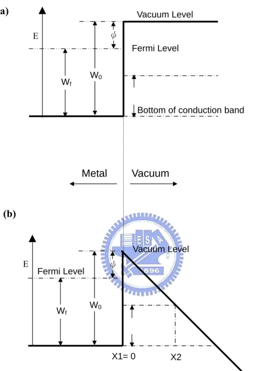
Electron field emission is a quantum mechanical tunneling phenomenon of electrons extracted from the conductive solid surface, such as a metal or a semiconductor, where the surface electric field is extremely high. If a sufficient electric field is applied on the emitter surface, electrons will be emitting through the surface potential barrier into vacuum, even under a very low temperature. In contrast, thermionic emission is the hot electron emission under high temperature and low electric field. Fig. 1-1(a) demonstrates the band diagram of a metal-vacuum system.
Here W0 is the energy difference between an electron at rest outside the metal
and an electron at rest inside, whereas Wf is the energy difference between the Fermi
level and the bottom of the conduction band. The work function φ is defined as φ = W0 - Wf. If an external bias is applied, vacuum energy level is reduced and the
potential barrier at the surface becomes thinner as shown in Fig. 1-1(b). Then, an electron having energy “W” has a finite probability of tunneling through the surface barrier. Fowler and Nordheim derive the famous F-N equation (1.1) as follow [1.4]:
( )
exp[ 2 ( )/ ] 3 2 E y v b aE J = − φ , (1-1)where J is the current density (A/cm2). E is the applied electric field (V/cm), φ is the work function (in eV), a = 1.56×10⁻⁶, b = -6.831×10⁻⁷, y = 3.79x10-4×10-4E1/2/φ,
t2(y)~1.1 and v(y) can be approximated as [1.12]
v(y)=cos(0.5πy), (1-2) or ( ) 0.95 2. y y v = − (1-3)
Typically, the field emission current I is measured as a function of the applied voltage V. Substituting relationships of J = I/α and E = βV into Eq.(1-1), where α is the emitting area and β is the local field enhancement factor of the emitting surface, the following equation can be obtained
exp[ ( ) ] ) ( 2 3 2 2 2 V y bv y t V A I β φ φ αβ − = . (1-4)
Then taking the log. form of Eq. (1-4) and v(y) ~ 1
] 2.97 10 ( ( )) ) ( 10 54 . 1 log[ ) log( 2 3 7 2 2 6 2 V y v y t V I β φ φ αβ − × × = − , (1-5)
from Eq. (1-5), the slope of a Fowler-Nordheim (F-N) plot is given by
2.97 10 ( 2) 3 7 β φ × = ≡slopeFN S , (1-6)
The parameter β can be evaluated from the slope S of the measured F-N plot if the work function φ was known
2.97 10 ( 2) 3 7 S φ β =− × (cm-1). (1-7)
The emission area α can be subsequently extracted from a rearrangement of Eq. (1-5)
exp( 9.89)exp(6.53 10 ) 10 4 . 1 ) ( 2 3 7 2 6 2 V V I β φ φ β φ α − × × = − (cm2). (1-8)
For example, the electric field at the surface of a spherical emitter of radius r concentric with a spherical anode (or gate) of radius r+d can be represented analytically by ( ) d d r r V E= + . (1-9)
Though a realistic electric field in the emitter tip is more complicated than above equation, we can multiply Eq.(1-9) by a geometric factor β` to approximate the real condition. Etip ≡function of (r,d) =β` ( ) d d r r V + , (1-10)
where r is the tip radius of emitter tip, d is the emitter-anode(gate) distance and β` is a geometric correction factor [1.13].
And for r>>d, Etip approaches to β`(V/d) which is the solution for a parallel-plate
capacitor and for a diode operation in a small anode-to-cathode spacing.
As the gated FEA with very sharp tip radius, Eq. (1-10) can be approximated as:
Etip =β`(V/r). (1-11)
Combining E = βV and Eq. (1-11), we can obtain the relationship:
Etip =βV =β`(V/r), and β`= βr. (1-12)
The tip radius r is usually in the range from a few nm to 50 nm, corresponding to the parameter β` ranging from 10-1 to 10-2.
Besides, transconductance g of a field emission device is defined as the change m
in anode current due to the change in gate voltage [1.3] and is expressed as:
g C m V I g ∂ ∂ = |Vc. (1-13)
Transconductance of an FED is a figure of merit that gives as an indication of the amount of current charge that can be accomplished by a given change in grid voltage. The transconductance can be increased by using multiple tips or by decreasing the gate-to-cathode spacing for a given anode-to-cathode spacing.
approaches may therefore be taken to reduce the operating voltage of the field emission devices:
1) Find techniques to reproducibly sharpen the tips to the atomic level (increaseβ).
2) Lower the work function of the tip (φ).
3) Narrow the cone angle (increaseβ).
1.2 The Structure and Technology Trends for Field Emission Display
1.2.1 Applications of Vacuum Microelectronics
Due to the superior properties of vacuum microelectronic devices, potential applications had been invented, including high brightness flat-panel display [1.14-1.18], high efficiency microwave amplifier and generator [1.19-1.21], ultra-fast computer, intense electron/ion sources [1.22-1.23], scanning electron microscopy, electron beam lithography, micro-sensor [1.24-1.25], temperature insensitive electronics, electron/ion sources, excitation sources, and radiation hardness analog and digital circuits.
Among wide range applications of the vacuum microelectronics, flat-panel display exhibits superior advantages inclusive of super thin panel, high brightness, high contrast, large view angles, high response speed, low driving voltages, low power consumption, and a self-luminary. Most importantly FPD can be operated in the worst environment compared to the solid state electronics. Fig. 1-2 showed the applications of flat panel display.
Various kinds of flat-panel displays can be classified into two groups: Emissive and Non-Emissive type. Liquid crystal display (LCD) belongs to the Non-Emissive type. However, organic light emission display (OLED), vacuum fluorescent display
(VFD), plasma display panel (PDP), and field emission display (FED) belong to the Emissive type. They all were developed for the better characteristics of small volume, light weight, and low power consumption.
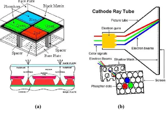
LCDs have some drawbacks. First, the poor response speed results from the relationship between liquid crystal, environment temperatures, and operation voltages. Second, low brightness and high costs arise from the backlight model. Last, the view angle is not large. However, based on the mature semiconductor technology, LCDs are most popular displays in the world. OLEDs have many advantages, such as no needs for the backlight model, low cost, low power consumption, high view angles, high contrast, and high response speed. Most importantly OLEDs can be fabricated to be a full color and large scale panel, even for the flexible panel applications. But, OLEDs should overcome the worst drawback “short life time”. The theory of luminesce of FEDs is very similar to the Cathode Ray Tube (CRT). The cathode of CRT generates thermionic electrons by heating, then offset voltages accelerate and concentrate the electrons, then the magnet controls the direction of electrons, and electrons scan the phosphor back and forth. The anode of FED can be applied at suitable turn-on electrical field and the cathodes emit electrons based on the FN tunneling. FED features all the pros of the CRTs in image quality and possesses flat
As the all of the above saying and the Table 1.2, FEDs possess the advantages, such as low weight and small volume, high brightness, high contrast, large view angles, high response speed, low driving voltage, low power consumption, self-emission, and normal operation in the worst environment. But, some critical issues should be overcome like short life time, uniformity and stability of emission currents, and vacuum package. However, in the display field, LCDs and PDP still dominate the market of the small and large panel display, respectively. With the revolution and innovation of new technology, we believe FEDs will be a promising display in the future.
1.2.2 Cold Cathode Structures and Materials for Field Emission
Display
With the improvement on the semiconductor fabrication technology, FED is one of the most promising applications of flat panel displays, which can overcome the drawbacks of TFT-LCD. The features of FEDs are small volume, low power consumption, fast response speed, color performance similar to CRT, large view angles, and low cost. Otherwise, FEDs have some drawbacks, such as the uniformity of brightness, high breakdown voltage, the package spacer charging, short life time, and vacuum package, which are all serious problems. In the past 30 years, so many applications of FEDs were demonstrated by the academia and noted laboratories.
Table 1.3 showed the comparison of the FEDs. Based on the emitting methods, we could separate the FEDs into two groups: direct and fractional emitters. The CNTs and Spindt type can emit electrons directly from the emitters, so they belong to the direct emitters. Moreover, the BSD, MIM, and SED emit electrons form dispersed nano-particles of the thin films, and they belong to the fractional emitters.
A. Spindt-Type Field Emitters
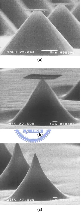
Since 1960s, the concepts of FEDs were demonstrated, and many scientists contributed their innovation to the FED applications. Ken Shoulders published the first micro-electric device based on the F-N tunneling theory [1.26]. However, Capp Spindt who successfully fabricated and operated the FEA (Field Emission Array) contributed the semiconductor technology to the vacuum microelectronics, called the Spindt-type cold cathode [1.7]. The Spindt-type is micro-meter scale emitters and possess self aligned metal pyramids and gates [1.27]. The Fig. 1-4 was Spindt-type triode structure fabricated by Capp Spindt. From then on, many applications of FEDs were demonstrated by the academia and noted laboratories. The Spindt-type has some advantages, such as high thermal stability, high emission reliability, low cost, and larger area displays of many tip arrays. In addition, the most importance is Spindt-type can be easily fabricated in the general semiconductor fabrication
However, the most popular Spindt-type material is silicon tip emitters. Fig. 1-5 is silicon tip diagrams. The most desirable characteristics of silicon tips are the low operation voltage, emission stability, long durability, and high emission current density. These properties are strongly dependent on the tip curvature radius (related to the field enhancement factor), emission material (determines the work function), and surface conditions. According to Eq.(1-1), the methods to enhance the emission currents are increasing the work function of cathode materials and increasing the field emission factor (β). We had to decrease the work function of silicon tips and coat conduction layers, such as DLC (Diamond Like Carbon), carbon films, Mo….etc [1.9-1.11,1-29]. Conduction layers can decrease the silicon work function and enhance the emission efficiency. However, there are some existing drawbacks of Spindt type field emitters when fabricating Spindt type FED such as (1) high gate driving voltage required; for a Spindt type field emission triode with 4 μm gate aperture, the driving voltage is typically more than 60 V, which results in the high cost of the driving circuits. To reduce the gate driving voltage, (1) frontier lithography technologies such as E beam lithography must be applied to reduce the gate aperture to the sub-micron level and (2) huge and expensive high vacuum deposition system is required during fabricating large area Spindt type FED.
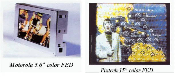
based on Spindt type field emitters such as Futaba, Sony/Candesent, Futaba and Pixtech [1.30], the products above mentioned companies were shown in Fig. 1-6.
B. BSD Field Emitters
BSD (Ballistic Electron Surface Emitting Device) was developed by Panasonic and Tokyo University of Agriculture and Technology. The operation diagram of BSD was shown in the Fig. 1-7. The PPS (porous poly-Si) of cathodes of BSD have micro-crystal particles, which have a thin oxide film on itself. The offset voltages are applied between the anode and cathode, the electrons emitted by the cathode inject into the PPS, the electrons accelerated by the PPS interactions gain high energies and emit, and the emission efficiency of electrons is about 2%. Because the external voltages are focused on the oxide surface of the micro-crystal particles, then the thin film surface forms strong electrical fields, and the electrons can be emitted. However, the phenomenon called “Ballistic Electron Conduction”. In addition, the high active electrons are emitted from the cathode in the vertical direction without the deviation adjustment. The BSD has the advantages, such as simple structures, but it is very sensitive to the ion bombardments and has serious drawbacks like the poor emission efficiency.
MIM [1.31] (Metal Insulator Metal) technology was investigated by Hitachi and LGE, but they didn’t publish the detailed technology researches. According to the paper survey, MIM technology is the hot electron generation in the dielectric and the structure are shown in Fig. 1-8. The features of MIM are the low degrees of electron dispersion, low driving voltages, and high current density, but it is easily affected by the ion bombardments. However, the structure and fabrication of MIM are very complicated.
D. SCE Field Emitters
Canon and Toshiba co-operated the whole new 36 inches planar panel display called “SCE (Surface Conduction Emitter)” and published a plan for large productions in Sep 14 2004 [1.32]. Fig. 1-9 was the base structure of SCE. At SID 2005, Canon showed the SCE display specifications, including 400 cd/m2 peak
luminance, high contrast about 10000:1, response speed below 1ms, and panel thickness about 7.3 mm. By the way, it showed the superior emission stability
As Fig. 1-9, the mechanism of emission of SCE is the external voltage is applied on the PdO particles located in the extreme narrow gaps, the electrons emit from the extreme narrow gaps based on tunneling effect, and electrons hit onto the phosphors of anodes. Moreover, the PdO thin film was coated by the ink-jet methods, and its
thickness was about 10nm. The currents passed through the PdO thin film and about 2% electrons emited into the vacuum. Its emission efficiency compared to other field emission emitters is much better. The features of SCE are the simple structure, low cost and large panel display. But, in accord with the other FEDs, some essential properties like stable emission currents, low driving voltages, low cost fabrications, and longer operation life are still needed to be resolved.
1.3 The Promising Field Emission Technology – Carbon Nanotubes
Since the discovery of carbon nanotubes (CNTs) by Iijima in 1991, [1.33] CNTs have attracted considerable interests because of their unique physical properties and many potential applications [1.34]. CNTs have numerous potential applications in nanoelectronics, nanometer-scale structural materials, hydrogen storage, field-emission devices, and so on. Among these applications, CNTs seem to be very promising as electron emitters for field-emission displays (FEDs).1.3.1 The Synthesis Methods of Carbon Nanotubes
Carbon nanotubes (CNTs) have been extensively investigated for the synthesis using arc discharge, laser vaporization, pyrolysis, solar energy, and plasma-enhanced chemical vapor deposition (CVD), for its unique physical and chemical properties and for applications to nanoscale devices. However, common methods of CNT synthesis include: (1) arc-discharge [1.35], (2) laser ablation [1.36], (3) thermal CVD [1.37-1-39], and (4) plasma enhanced CVD [1.40-1-41].
The laser ablation can synthesize pure carbon nanotubes in high fabrication temperature, but large scale display panel can not be fabricated in the high fabrication temperature above the melting point of glass substrate. The arc discharge can synthesize carbon nanotubes in shorter fabrication times, but it has some issues, such
as (1) poor purity, (2) hard to control growth orientations of carbon nanotubes, and (3) poor emission uniformity. Compared to laser ablation and arc discharge, using CVD for carbon nanotube growth has some features, such as (1) high purity carbon nanotubes, (2) selective growth only for catalyst metal, (3) controlling growth direction, and (4) much suitable to semiconductor fabrication procedure. However, with the display technology trend, it is the time for large panel display. We need to synthesize carbon nanotubes using CVDs on large panel substrates. For this reason, carbon nanotube growth at low temperatures is unavoidable, but the purity of carbon nanotubes at low temperatures is poor. So, we still try some methods to increase growth rates at low temperatures, such as (1) multilayer catalysts, (2) plasma CVDs, (3) post-treatment, and so on.
1.3.2 Applications of Carbon Nanotubes
Since the discovery of CNTs in 1991, CNTs had attracted much attention for their unique physical and chemical properties. Their extensively potential applications lead them to become a super star of nano technology, which cover: (1) Chemical sensor [1.42], (2) IR detector, (3) Nano-conducting Wire, (4) Vehicles for Hydrogen Storage [1.43], (5) Field Effect Transistor [1.44], (6) Field Emission Display (FED), (7) Probe of AFM and etc.
In the wide-ranging applications of CNTs, FED arouses researchers’ interest particularly. In virtue of the superior field emission characteristics, CNTs are applied to the emitting source of cold cathode. The advantages of FED are its low response time, wide view angle, high brightness, high working temperature range and well combination with mature phosphor technology. However, a major problem needs to be solved in this field. It is not allowed to effectively analyze CNTs on a flat panel at relatively lower temperature (<500˚C) and this barrier restriction obstructs the development of CNT-FED so far.
1.4 Motivation
In the growth reaction of CNTs, the diffusion of carbon in the catalyst metal has been believed to be the rate-determining step. The growth rate of CNTs can be described by an Arrhenius equation that the activation energy is the diffusion energy of carbon in the metal [1.45]. According to the Fig. 1-10, PECVD is more suitable method for CNT synthesis because PECVD has the much lower activation energy compared to thermal CVD [1.46]. However PECVD has some drawbacks like plasma uniformity and large panel display fabrication.
There are many methods to enhance the growth rate of carbon nanotubes by thermal CVD, such as (1) finding out the catalyst alloys with the extreme low melting point, (2) nano-size particles preparation, (3) two zone heating method [1.47-1.48], and adding carbon atoms into the pretreatment [1.49-1.51] … and so on.
We have investigated the “nano-size” method to accomplish carbon nanotube growth at low temperature because its method has three advantages from paper survey. First, nano-size catalyst particles are more active compared to bulk catalyst metals and exhibit the nano-phenomenon effectively. Second, the melting point decreases as the catalyst particle sizes decrease [1.52-1.53]. In particularly, K.K. Nanda et al. [1.54] published the model for the relationship between melting point and particle
sizes….Co metal for example Fig. 1-11. Last, at low temperature the solubility of carbon atoms in catalyst metals is low, so the amount of carbon diffusing through the particles is very limited. This suggests growth occurs by surface diffusion of carbon on catalyst metals [1.55-1.56]. As the Fig. 1-12, surface diffusion or surface premelting of nano-size particles takes place when the temperature is raised above 500ْ C whose temperature is close to 0.4Tmb. We supposed that the multilayered catalytic films which can form nano-particles have all the above advantages and synthesized the carbon nanotubes at low temperature (400ْ C). In addition, we hoped the surface diffusion mechanism of carbon nanotubes using multilayered catalytic films could be realized by thermal CVD. The Fig. 1-13 is the growth mechanism of carbon nanotubes using multilayered catalytic films.
A multilayer catalyst, Co/Ti/Al, was successfully employed to synthesize CNTs at 550℃ and 500℃ by thermal CVD previously. But morphologies and field emission characteristics are not as good as we thought. Therefore, the priority work is optimum of CNTs using Co/Ti/Al at the low temperature to improve the characteristics of CNTs. Then, using the optimum condition drives down the growth temperature.
The phosphors provide high efficiency into light by bombardments of electrons at enough high voltages of the anode plate. The high-anode voltage improves the qualities of FEDs in color purity and high brightness. The high-anode voltage requires
a large vacuum gap between the cathode and anode plates. The large vacuum gap may cause a problem of beam spreading. Therefore, a focusing structure which could well control the trajectory of electrons and reduce the cross-talk noisy is necessary. Several focusing structures of FED have been announced to overcome the issue of electron spreading, such as planar-electrode type (Fig. 1-14), double-gate type (Fig. 1-15), and mesh-electrode type (Fig. 1-16). Those structures have some drawbacks, such as the complication in the manufacturing process and the reduction in emission current owing to the focusing electrodes.
In this thesis, a self-focusing gate structure is fabricated with simple fabrication processes, and the results of the simulation and luminescent images shows a good controllability in electron trajectory. This novel triode structure with simple processes is promising for the application of FED. We only change the shape of the gate to get the focusing effect. It is simple, but work well.
Chapter 2
Study on the Carbon Nanotubes Synthesized Using
Co/Ti/Al Multilayer Catalyst at Low Temperatures
2.1 Introduction
First of all, we used titanium as the interlayer of the multilayer catalysts for CNT synthesis because it was found the most fitting one for CNT growth at low temperatures. Then, we fabricated diode structure on silicon substrate to improve the morphologies of CNTs. Our group has done the research on multilayer catalysts, but the characteristics were not as good as we thought. So it is important to optimize CNTs at low temperature. Finally, we accomplished kinds of analysis for the above mentioned. The scheme of the whole experimental procedures was shown in Fig. 2-1.
2.2 Experimental Procedure
An n-type silicon wafer with (100) orientation was prepared for the substrate. After the RCA clean and lithography processes, we defined three kinds of patterns (squares of 1000、 100、10 um2) for CNT field emission arrays. A 2000 Å Cr layer was deposited by dual E-gun evaporation (JAPAN ULVAC EBX-10C) as the cathode between the substrate and catalysts. The multilayer catalyst (Co/Ti/Al) formed of Al (10 nm), Ti (3 nm), and Co (2 nm) were sequentially deposited on substrates by magnetron sputtering (Ion Tech Microvac 450CB) at the pressure of 7.6×10⁻² Torr at room temperature. Because the sputtering system consisted of three sputtering sources, the multilayer catalysts could be sequentially sputtered without breaking the vacuum environment.
The atmospheric pressure thermal CVD system consists of a 2-in.-diameter horizontal quartz tube, an electric heating system, reaction gas supply and related mass flow controllers (Fig. 2-2). Samples loaded into the quartz tube were heated to the predetermined temperatures in the range from 370 to 750 ℃ in a nitrogen flow as an oxygen-free ambient. Prior to the CNT growth, hydrogen gas with a flow rate of 50sccm was fed into the reaction tube for 5 min to reduce the catalyst metal to the metallic phase, meanwhile transforming into nanoparticles. Then, carbon nanotubes were grown at designated temperatures with reaction gas, ethylene, at a flow rate of 50sccm for 30 mins; with nitrogen and hydrogen were introduced. After that, samples were furnace-cooled to room temperature in nitrogen flow to
The morphologies of the samples were characterized by scanning electron microscopy (SEM; Hitachi S-4700I). The fine internal structures of nanotubes and catalytic elements of nanoparticles were examined by high-resolution transmission electron microscopy (HRTEM; JEOL JEM-2000EX) and X-ray energy dispersive spectroscopy (EDS), respectively. Field emission characteristics of CNTs were measured with a parallel diode-type configuration in a high-vacuum chamber with the pressure of 5×10⁻⁶ Torr. A glass substrate coated with indium tin oxide (ITO) and P22 phosphor (ZnS: Cu, Al) was used as the anode plate, and the gap between the cathode and the anode plate was set to be 160 μm. The emitting area was well defined as 0.25 mm2 by photolithography. Anode voltages up to 1000 V were applied at intervals of 5 V with a source measure unit (Keithley 237) (Fig. 2-3) for the verification of field emission characteristics while the cathode was biased at 0 V.
2.3 Experimental Design
2.3.1 Optimization of CNTs Grown using Co/Ti/Al Multilayer Catalyst
Films
In order to achieve an effective growth of CNTs, it is very important to maintain the optimum carbon concentration in the catalyst by controlling the flow rate of ethylene, hydrogen and nitrogen. The multilayer catalyst (Co/Ti/Al) formed of Al (10 nm), Ti (3 nm), and Co (2 nm) were sequentially deposited on substrates by magnetron sputtering. The whole experimental process was presented schematically in Fig. 2-4. Prior to CNT growth, the catalysts’ nano-films were pretreated at 500℃ for 5 minutes with 50 sccm H2, and for 5
minutes with 1000sccm N2, respectively. Then, we try the different flow rate of N2, H2 and
C2H4 to grow CNTs at 500℃ for 30 minutes. First, the growth recipes were fixed the flow rate
of C2H4 with 75 sccm and changed the ratio of the flow rate of H2 and N2 between 0/1000 and
50/950to find out the best flow rate of the H2 (Fig. 2-5). Next, we change the flow rate of N2
ranged from 0 sccm to 5000 sccm to find out the best flow rate of N2 (Fig. 2-6). Afterwards,
we fixed the flow rate of N2 and N2 and changed the flow rate of C2H4 ranged from 25 sccm
to 138 sccm (maximum value) (Fig. 2-7). Finally, this method should be successful to find out the optimum flow rate of reaction gases grown CNTs using multilayer catalyst films with Ti interlayer at 500℃.
The growth recipe and samples are the same as 2.3.1 for stress test. The electric characteristics are measured by Keithley 237 in a 10-6 torr chamber for stress test by 1 hr. We also applied an ITO glass with phosphor coating on it as the anode to observe the luminescent image.
2.3.3 Determined Activation Energy for Co/Ti/Al Multilayer Catalyst
It has been shown that the activation energy characterized for the growth of CNTs by PECVD was lower than that by thermal CVD [2.1] and that the growth limiting step was determined by the diffusion of carbon on catalysts: surface diffusion for PECVD and bulk diffusion for thermal CVD [2.2]. This indicates that effective decomposition of carbon precursors by plasma could enhance the growth rates at low temperatures due to a lower activation energy. Since thermal CVD utilizes thermal energy to assist the decomposition of carbon precursors, a highly active catalyst with a low activation energy is essential for low-temperature synthesis of CNTs. Moreover, the investigation of the activation energy of CNTs grown with highly active catalysts in a thermal CVD system is also necessary for the clarification of the growth mechanism. The multilayer catalyst (Co 2 nm/Ti 3 nm/Al 10 nm) Samples loaded into the quartz tube were heated to the predetermined temperatures in the range from 370 to 700 ℃ in a nitrogen flow as an oxygen-free ambient. Prior to the CNT growth, hydrogen gas with a flow rate of 50sccm was fed into the reaction tube for 5 min to reduce the catalyst metal to the metallic phase, meanwhile transforming into nanoparticles.
Then, carbon nanotubes were grown at designated temperatures with reaction gas, ethylene, nitrogen and hydrogen at the flow rate of optimum value determined by 2.3.1. After that, samples were furnace-cooled to room temperature in nitrogen flow to fully exhaust the reaction and byproduct gases.
2.3.4 Determined Activation Energy of Single and Bilayer catalyst
For comparison, a conventional catalyst of Co with the thickness of 2 nm and the bilayer catalyst (Co 2 nm/Ti 3 nm and Co 2 nm/Al 3 nm) were used as reference samples. The nano-films of catalysts were pretreated for 5 minutes with 50sccm H2, and for 5 minutes with
1000sccm N2, respectively. Then, the optimum flow rate of C2H4, H2 and N2 was added to
grow CNTs at temperatures ranged from 370℃ to 700℃ for 30 minutes.
2.3.5 AFM Analysis
The growth samples are multilayer catalyst (Co/Ti/Al), bilayer catalyst (Co/Ti and Co/Al) and single layer catalyst (Co) as the same thickness mentioned before. The samples are pretreated the 50sccm hydrogen for 5 minutes, then 1000sccm nitrogen for 5 minutes. Finally, the samples are analyzed by AFM for investigation the surface roughness.
2.4 Results and Discussion
2.4.1 Effects of the Flow Rate and Gases
Figure 2-8 (a)-(d) show cross-sectional SEM images of samples deposited at different H2/N2 Ratio for the multilayer catalyst (Co/Ti/Al). The corresponding tilt-view image of each
sample is shown in the inset. It is clear that the length of nanotubes are changed from different H2/N2 ratio and that the cross-sectional morphology changes from short spaghetti-like
orientation to vertical forest-like alignment to amorphous carbon film. For experiments where only ethylene is present or adds hydrogen, morphologies are also very different. Thus it appears that atomic hydrogen is important to growth. Excess amounts appear to result in slower growth CNTs and deposition of the amorphous carbon film. Optimum growth rates are likely to be achieved with specific ratios of hydrogen and nitrogen. Surprisingly, the growth rate is less when hydrogen is provided increasingly. This may result from increased levels of atomic hydrogen can act to reduce the rate of decomposition of ethylene on the catalyst surface, but increase the rate of deposition of amorphous carbon(Fig. 2-8(d)). However, if we don’t provide hydrogen (Fig. 2-8(a)), there are some amorphous carbon deposited and morphology of CNTs are not good. Therefore, it is a critical role for hydrogen and sensitive to its flow rate. This means that the hydrogen plays a crucial role in the growth of carbon nanotubes, since it dilutes the ethylene gas and cleans the surface of the catalyst.
samples. The G peak and D peak located on 1580 cm-1 and 1350 cm-1. It is well known that the Raman spectrum monitors the state of the sp2-bond and sp3-bond graphite structure. Most of the carbon atoms in graphite form a sp2-bond matrix (G) and the remainders are sites (D). It is very clear that the sample of the ratio of 10sccm hydrogen and 990sccm nitrogen has the best morphology (Fig. 2-8(b)) and characteristics (Table 2.1). So we find out the property flow rate of hydrogen may be 10sccm.
Figure 2-11 (a)-(i) show cross-sectional SEM images of samples deposited at different flow rate of N2 for the multilayer catalyst (Co/Ti/Al). The corresponding tilt-view image of
each sample is shown in the inset. It’s obvious that the optimum flow rate of nitrogen is 1000 sccm. Other group says the nitrogen in CNT growth or bamboo-like CNT formation is basically to prolong the passivation of the front catalyst surface to enhance carbon diffusion [2.3]. However, we think the nitrogen is only the role of the carrier gas but nothing else. When its flow rate is too less (Fig. 2-11(a)-(c)), the amorphous carbon is deposited and morphologies are bad. When its flow is too much, the hydrocarbon gas dilutes with too much nitrogen so that the morphologies are not so well (Fig. 2-11(f)-(i)). Fig. 2-12 and Table 2.2 are the field emission characteristics for different flow rate of nitrogen and the Fig. 2-13 is Raman spectrum. The results are obviously clear that the optimum flow rate of the nitrogen is 1000 sccm.
flow rate of C2H4 for the multilayer catalyst (Co/Ti/Al). It’s clear that the ethylene is source of
the carbon atoms. There must be some trade off flow rate of C2H4. Too much (Fig. 2-14(g)) or
too less source gas (Fig. 2-14(a)-(c)) is not good for CNTs growth. Too less ethylene is not sufficient carbon atoms for CNTs growth. On the contrary, too much C2H4 is deposited
amorphous carbon film. Fig. 2-15 shows the evidence that the proper flow rate of C2H4 effect
the crystallization of CNTs and the field emission characteristic (Fig. 2-16) is correspondent to the Raman spectrum. The lower ID/IG is, the better field emission characteristic is. The best
field emission current density reach to 26.5 mA/cm2 at 6.25 V/um and turn-on voltage is relatively low (Table 2.3).
According to the results above, we decide the flow rate of hydrogen is 10 sccm, 1000 sccm for nitrogen and 125 sccm for ethylene. The rest of experiments will utilize this optimum value and change the growth time.
The thermal CVD method has been used to investigate the effects of hydrogen. It appears that atomic hydrogen is important to both nucleation and growth. Optimum growth rates are likely to be achieved with specific flow rate of hydrogen, nitrogen, and ethylene. The growth rate is less when only C2H4 is provided without the presence of hydrogen. Excess amounts
appear to result in slower growth rates and form the carbon films. As a results, the role of hydrogen during catalyst pretreatment and stage of CNT growth is to promote nano-particle agglomeration and activate the catalyst. The presence of nitrogen can enhance the carbon
dilution and diffuse in the catalyst surface. But, too much N2 gas caused over-diluted.
Ethylene is nothing but only carbon source. The specific flow rates of the gases will influence the crystallization of the CNTs and growth rate.
2.4.2 Activation Energy of Multilayer, Bilayered and Single Catalyst
The growth samples are multilayer catalyst (Co/Ti/Al), bilayer catalyst (Co/Ti and Co/Al) and single layer catalyst (Co) as the same thickness mentioned before. The samples are pretreated the 50 sccm hydrogen for 5 minutes, then 1000 sccm nitrogen for 5 minutes and grow with optimum condition between 370℃ and 700℃. Fig. 2-17(a)-1(d) and Fig. 2-18(a)-1(h) show cross-sectional SEM images of samples deposited at different temperatures (370, 400, 450, 500, 550, 600, 650, and 700℃) for the conventional catalyst (Co) and the multilayer one (Co/Ti/Al), respectively. 450 to 700 grow 30 minutes. ℃ Only 370 and 400 ℃ grow 2 and 4 hours, respectively. The corresponding tilt-view image of each sample is shown in the inset. It is clear that the length of nanotubes increases with temperature. It is generally known that as the temperature increases, the activity of catalysts and reactivity of carbon precursors become higher, and thus the growth rates could be greatly enhanced. Therefore, more active nucleation sites could be formed at higher temperatures, resulting in higher densities of CNTs. A high nanotube nucleation density combined with fast growth rates would contribute to the vertical alignment of CNTs due to a steric effect (crowding effect): the confinement by neighboring nanotubes leads to a preferred growth direction perpendicular
to the substrates [2.4]. It is worth noting that CNTs could not be grown at the low temperatures of 400 and 370℃ for the samples of conventional catalyst (compared with those of the multilayer catalyst). Despite some curly or wavy nanotubes grown at different temperatures, a reasonable estimation of the average length and corresponding growth rates can be obtained from the cross-sectional images, and the average growth rate of CNTs as a function of temperature, that is, Arrhenius plots of growth rate (nm/s) vs 1/T (K-1), are plotted in Fig. 2-19, and used to derive the activation energy. The data fit well to a linear interpolation, providing an effective activation energy of 0.903eV for the multilayer catalyst, and the activation energy of 1.69eV for the conventional catalyst in this work is close to the diffusion energy of carbon for thermal deposition (~1.2-1.8eV) [2.2], whereas that for the multilayer catalyst is considerably lower.
Figures 2-20 and 2-21 show cross-sectional SEM images of samples deposited at different temperatures (500, 550, 600, 650, and 700℃) for the bilayer catalyst (Co/Ti) and the bilayer one (Co/Al), respectively. The data fit well to a linear interpolation, providing an effective activation energy of 1.04eV for the bilayer catalyst (Co/Ti), and the activation energy of 1.01 eV for the bilayer one (Co/Al) (Fig. 2-22).
Figure 2-23 shows HRTEM images of nanotubes grown with the multilayer catalyst at 400, 450, 500, 550, and 700℃, and reveals a closed tip filled with catalytic metal particles and a multiwalled structure consisting of the wavy graphite sheets aligned parallel to the tube
axis. The outer graphitic sheets are usually less crystalline than the inner ones, and more defects are shown in the outer surface of nanotubes. The corresponding EDS analysis of the catalytic particle is shown in Fig. 2-24, confirming that the particle is composed of cobalt. Neither Al nor Ti peak appears in the figure, and the Cu signal originates from the TEM microgrid. This result is similar to those of other literature in which binary catalysts were employed [2.5-2.6], and indicates that only Co particles directly participate in the growth of nanotubes and that Ti and Al thin films are not involved in the growth of nanotubes but have other functions instead.
2.4.3 Reliability for Electrical Stress Test
Figure 2-25 shows samples from 2.3.1 test for stress and Table 2.4 presents the statistic data. The reliability increase when the process gases tend to optimum flow rate. It is correspondent to Raman spectrum because the crystallized CNTs are more reliable than amorphous one.
2.4.4 Roles of Al and Ti Determined by AFM and SEM
An intermediate layer, Ti, is generally used as a buffer layer to improve the adhesion of nanostructured carbon films by the formation of chemical bonds with carbon, and hence stable carbide compound (TiC), according to the C-Ti phase diagram (Fig. 2-26).Moreover, we assume that Ti used as a co-catalyst tended to decrease the growth temperature of curled
decomposed by the Ti co-catalyst thin film provide more atomic carbon for Co catalytic nanoparticles, thereby enhancing the growth of carbon nanotubes at low temperatures. Therefore, the Ti intermediate layer serves as a growth-enhancing layer. Without the intermediate layer (Ti), nanotubes could not grow well at a low temperature of 500℃. Consequently, the employment of the Ti layer would effectively enhance the activity of catalysts at low temperatures.
Figure 2-27 shows the AFM images of the samples fabricated with the conventional catalyst, the bilayer catalyst and the multilayer catalyst, after pretreatment processes at 500℃. It is obvious that well-distributed nanoparticles could be achieved in the sample with the multilayer catalyst, whereas that prepared with the conventional catalyst shows unwell-distributed and even morphologies. It is conjectured that the thin aluminum layer transforms into aluminum oxide during the heating step due to the residual oxygen in the reaction chamber [2.7]. Jodin et al. [2.8] reported that catalysts combining with fumed alumina nanoparticles acting as a support could prevent agglomeration during the CVD growth process, that is, the alumina support facilitates the uniform distribution of the catalytic nanoparticles and preserves their small sizes for CNT growth. Moreover, compared with a flat substrate coated with metal catalyst clusters, a buffer layer-supported catalyst has the advantage of a higher active surface area, thus more active sites for nucleation [2.9-2.10]. The bilayer catalyst is worse than the multilayer one because it is lack of aluminum for uniform
distribute. And without Al, its surface roughness decreases (Fig. 2-27(b)). Therefore, aluminum is a good support layer for enhancing the growth of nanotubes. However, bilayer catalyst is better than single layer one. It is indirect to prove that the Ti layer improves the growth of CNTs by form TiC. From Fig. 2-28, the X-ray photoelectron spectroscopy (XPS) analyzes the TiC phase exist on multilayer catalyst after growth at 500℃. From the Fig. 2-29, the SEM images show the Al layer plays a role of the uniformity of the particles. Meanwhile, it can also be function as shrinking down the particle size. The results correspond to the AFM images.
Chapter 3
A Field Emission Device with the Novel
Self-Focusing Gate Structure
3.1 Introduction
In most of field emission device (FED) panels the phosphor materials used in CRT screens are still used. These phosphors provide high efficiency into light by bombardments of electrons at enough high voltages of the anode plate. The high-anode voltage improves the qualities of FEDs in color purity and high brightness. The high-anode voltage requires a large vacuum gap between the cathode and anode plates. The large vacuum gap may cause a problem of beam spreading. Therefore, a focusing structure which could well control the trajectory of electrons and reduce the cross-talk noisy is necessary. Several focusing structures of FED have been announced to overcome the issue of electron spreading, such as planar-electrode type [3.1], double-gate type [3.2-3.4], and mesh-electrode type [3.5]. In the double-gate type, a focusing electrode is stacked on the gate electrode with an additional insulating layer. In this structure the additional insulating layer is required to sustain electrical breakdown between gate and focusing voltages. If thick film is used as the insulating layer,
there may occur to several problems, such as the deformation of substrate due to the additional thermal process, the change of material property of gate electrodes, and difficulty of formation of CNT emitters within gate apertures.
The planar electrode locates on the coplane with the gate electrodes. This structure is simple in manufacturing process, but is restricted in high resolution. In the mesh-electrode type, a metal mesh is inserted between the cathode and anode. The mesh type is effective in focusing scheme, but could be restrictive in the extension to a large-size panel and difficulty in assembly.
In this chapter, a self-focus gate structure is fabricated with simple fabrication processes, and the results of the simulation and luminescent images shows a good controllability in electron trajectory. This novel triode structure with simple processes is promising for the application of FED. We only change the shape of the gate to get the focusing effect. It is simple, but work well. This can make this structure scalable in extension to a large-area panel and feasible in manufacturing high-resolution devices. This self-focus cathode structure is expected to have an excellent focusing effect in spite of the simple process and structure.
3.2 Simulations
3.2.1 Devices Design and Simulations
Simulations were performed to investigate the beam spreading of emission electrons with commercial software (SIMION-3D) using the finite element method. It was found that an initial energy and divergence angles of e-beams at the moment of emission from CNTs were 5 eV and -90°~+90°, respectively [3.6]. The thickness of silicon oxide layer formed by plasma-enhanced chemical vapor deposition (PECVD) is 1 μm. In simulations, emission of electrons is assumed on a flat surface of CNT emitters. The voltage between the cathode and anode plates is applied with 1 kV with the spacing of 550 μm, while the gate voltage is applied at 80 V.
The conventional device [3.7] has a surrounding gate so that electrons are emitted from the peripheral area of the extraction gate. Fig. 3-1 shows the cross-section view of the device. The spot size has strong relation to gate length. From Fig. 3-2, when the length of the extraction gate (red area) is ranged from 20um to infinite, the simulations are clear that the range of the electron beam from emission site (green area) is strongly related to the gate length which can change the electric potential. The red lines are equipotential lines.
It very clear that the gate length correlate to the electric potential which can influence the electron beam trajectories. So if there is a way to design a proper shape of the gate, the focusing effect may improve by easier method. The whole idea is that utilized a
non-symmetric gate area to impact the trajectories of the electron beam. Fig. 3-3 shows the emission sites (green area) are by the both side of extraction gate (red area). However, the focusing effect is unsatisfied. The problem is that extraction gate area is too large so that it creates too strong electric field. Therefore, if gate area can be designed properly, the focusing effect can be achieved.
Figure 3-4 shows the novel self-focusing structure which designs to achieve the focusing effect. The simulation (Fig. 3-5) reveals that is perfect impact on trajectories of the electron beam when the extraction gate splits into two pieces. The self-focusing gate structure has a symmetric extraction gate area, which consists of a pair of linear electrodes closed to the emission region of CNTs. The spot size shrinks down to the 232um. It is astonishing that can change the spot size so easily by this simple method.
Simulation results show that the self-focus structure has a spot size of 232 μm in length on the anodic plate, while conventional one has 622 um in length. It’s clear that the novel structure could effectively reduce the spot size on the anodic palate, therefore achieving a better focusing effect.


![Fig. 2-8 SEM micrographs of samples with the multilayer catalyst [(a)-(b)] after CNTs deposition processes at different H 2 /N 2 Ratio](https://thumb-ap.123doks.com/thumbv2/9libinfo/8227227.170782/85.892.126.762.142.707/micrographs-samples-multilayer-catalyst-deposition-processes-different-ratio.webp)
