Compact Microstrip Dual-Band Bandpass Filters
Design Using Genetic-Algorithm Techniques
Ming-Iu Lai, Student Member, IEEE, and Shyh-Kang Jeng, Senior Member, IEEE
Abstract—An optimization scheme based on hybrid-coded genetic-algorithm (GA) techniques is presented to design compact dual-band bandpass filters with microstrip lines. A representation scheme is proposed to represent an arbitrary microstrip circuit as a set of data structures. Each data structure in the set describes a simple two-port network with the corresponding connection method and electrical parameters. The optimization algorithm based on conventional GAs is then applied to simultaneously search for the appropriate circuit topology and the corresponding electrical parameters with dual-band characteristic. Two examples are designed and implemented to validate the proposed algorithm. In the first example, the 3-dB fractional bandwidth of the low and high bands is 35% and 17%, respectively. It has return losses larger than 10 dB from 2.14 to 2.96 and 5.14 to 6.06 GHz. In the second example, the 3-dB fractional bandwidth of the low and high bands is 9.9% and 7.9%, respectively. The return losses are larger than 10 dB from 3.37 to 3.64 and 5.27 to 5.62 GHz. The sizes of the proposed filters are nearly half as small as those of the filters presented before. All the studies are completed on a computer with a 2.4-GHz microprocessor, and the computing time of two examples is 6 and 3 min, respectively.
Index Terms—Bandpass filters, circuit topology, genetic algorithm (GA), microstrip circuit.
I. INTRODUCTION
W
IRELESS products such as wireless local area networks (WLANs), Bluetooth, etc. gradually become standard facilities in notebooks. In order to pursue more convenient and compact products, the demands for multifunctional RF trans-ceiver systems increase dramatically. In this trend, the devel-opment of multifunctional components like antennas and fil-ters plays an important role. In theory, a dual-band bandpass filter can be realized by cascading a bandpass and bandstop filter [1]. Nevertheless, this design approach is confronted by two difficulties. First, the bandpass filter needs to be with very wide passband if the ratio of the high-band central frequency to the low-band central frequency is high. Second, since the band-pass and bandstop filters are designed separately and then cas-caded to fulfill the dual-band characteristics, the resultant cir-cuit topology is large in size and, therefore, fails in compactManuscript received December 8, 2004; revised June 22, 2005. This work was supported by the National Science Council, Taiwan, R.O.C., under Grant NSC 93-2213-E-002-091 and by the Department of Industrial Technology, Ministry of Economic Affairs, Taiwan, R.O.C., under Technology Development Program of Academic 93-EC-17-A-05-S1-020.
M.-I. Lai is with the Graduate Institute of Communication Engineering, National Taiwan University, Taipei, 10617 Taiwan, R.O.C. (e-mail: milai1102@yahoo.com.tw).
S.-K. Jeng is with the Graduate Institute of Communication Engineering and the Department of Electrical Engineering, National Taiwan University, Taipei, 10617 Taiwan, R.O.C. (e-mail: skjeng@ew.ee.ntu.edu.tw).
Digital Object Identifier 10.1109/TMTT.2005.860327
design. Wada et al. [2], [3] studied the behavior of open-ended resonators and their application to microwave filters. They suc-cessfully applied the open-ended resonators and some lumped capacitors to design a bandpass filter with two narrow passbands [4]. However, their filter was simulated using ideal lumped ca-pacitors and there was no measured result. When realizing the filter, the use of chip capacitors may degrade the circuit’s per-formance and cause some unwanted effects. Accordingly, new methods to design compact and high-performance dual-band bandpass filters are highly desirable.
Various optimization techniques such as the gradient-based method [5], space mapping [6], [7], and neural networks [8] are available to design microwave circuits. Hsu and Huang [9] proposed a simulated annealing algorithm to design dual-wide-band microstrip line filters for WLAN applications. This ap-proach worked on the electrical parameters based on a given cir-cuit topology. A great deal of effort has been made on searching for the design parameters based on a given circuit topology. Only a few attempts thus far have been made at developing an algorithm capable of searching for the circuit topology, as well as the electrical parameters simultaneously.
Genetic algorithms (GAs), first introduced by Holland in 1975, have been widely used in science and engineering prob-lems [10], [11]. It also proves to be useful for solving complex electromagnetic problems [12]–[18]. For microwave filters synthesis, Peik and Chow [16] focused on searching for the optimal electrical parameters based on a given circuit topology. Nishino and Itoh [17], [18] proposed a scheme to describe the physical parameters and topology of the circuit composed of microstrip-line segments and then integrated this representation scheme with conventional GAs. Many filters with several pass-bands and stoppass-bands were presented. Nevertheless, since the representation scheme merely modeled the transmission-line segments with equal width and open-circuited shunt stubs, it is difficult to realize dual-band bandpass filters with sharp cutoff in the passbands, as well as good rejections in the stop-bands. The goal of this paper is to then explore an efficient computer-aid tool, which does not require human intervention, to synthesize dual-band bandpass filters including the circuit topology, as well as the corresponding electrical parameters.
As a beginning, a scheme is proposed to represent an arbitrary microstrip circuit as a set of data structures. Each data structure in the set describes a simple two-port network with the corre-sponding connection method and electrical parameters. The op-timization algorithm based on conventional GA is then applied to simultaneously search for the appropriate circuit topology and the corresponding electrical parameters with a dual-band characteristic. The details of the algorithm are addressed in
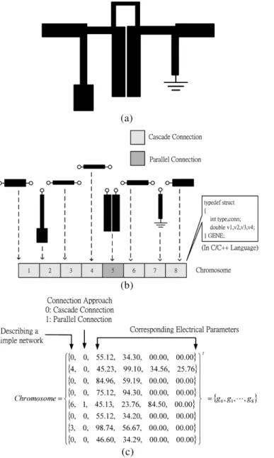
Fig. 1. Representation scheme in the proposed algorithm. (a) A typical passive microstrip circuit. (b) Decomposition of the circuit in (a) into basic circuit elements. (c) Chromosome of the circuit in (a), a set of structures.
tion II. Section III demonstrates two compact dual-band band-pass filters to validate the algorithm. Finally, some conclusions are given in Section IV.
II. THEORY
A. Representation Scheme
As illustrated in Fig. 1, an arbitrary two-port microstrip circuit [1], [19]–[22] can be decomposed into basic circuit elements. The data structure shown in Fig. 1(b) is then applied to describe such a basic circuit element. It is composed of three parts. The first part is coded in an integer representing the topology of a basic element. The second part is coded in an integer representing the way of connection to the previous ele-ment. The third part consists of many real numbers describing the corresponding electrical parameters of the element. Table I lists the details of the basic circuit elements. In the algorithm,
TABLE I
DETAILS OF THEBASICELEMENTS IN THEPROPOSEDALGORITHM
we define a structure as a gene and a set of structures as a
chromosome. A special gene called Empty is introduced, which
enables the representation scheme to be capable of describing a circuit with an arbitrary number of basic circuit elements and orders. With this approach, an arbitrary two-port network can be represented by a set of structures. The design problem can be formulated as
(1) where denotes a chromosome, as illustrated in Fig. 1(c), and is the scattering matrix obtained by electromagnetic sim-ulation. is the objective function to be minimized and is the appropriate chromosome.
B. Design Constraints
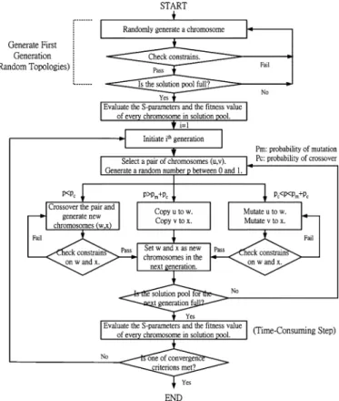
During synthesis in order to avoid unreasonable electrical pa-rameters in a chromosome, it is necessary to assign upper and lower limits according to various designs. The flowchart of the constraint testing is shown in Fig. 2. The first step is to check the values of electrical parameters in a chromosome. Since a ran-domly generated chromosome may represent an unreasonable network, additional attention should be paid in advance to iden-tify whether the circuit topology is a reasonable network and to remove the troublesome chromosome from a solution pool. For example, if the way of connection of a circuit element is parallel, but the circuit topology of the previous element is a shunt ele-ment, it is trivial to calculate the frequency responses for such a circuit topology. The junction problem is another issue when realizing a chromosome to a real microstrip circuit. Common junctions in microstrip circuits are step-, tee-, and cross-junc-tions, and others may result in problems in circuit implemen-tation. The algorithm for checking the circuit topology repre-sented by a chromosome is shown in Appendix A. For the chro-mosomes representing a reasonable network, user-defined con-straints such as the area of a circuit and the number of stubs are
Fig. 2. Flowchart for constraint testing.
then checked. These constraints are defined according to indi-vidual design requirements.
The following step is to check the location of the transmis-sion zero, which falls within the bandstop regions. From this step, we can easily predict the electrical performance of a ran-domly generated chromosome. This procedure not only sieves out the inferior chromosome from a solution pool, but also saves the computing time for evaluating the frequency responses of a circuit. For a chromosome with an open- or short-circuited shunt stub, the location of the transmission zero can easily be deter-mined by
for type (2)
for type (3)
for type (4)
for type (5)
where , , and are the electrical length of the stubs in ra-dians, denotes the reference frequency, and .
C. Definition of Fitness Value
The transmission-line models are used to calculate scattering parameters in order to effectively evaluate the frequency re-sponse of a chromosome. The algorithm for evaluating the scat-tering parameters of a chromosome is shown in Appendix B. The fitness value is defined by
(6)
where represents the weighting value at the th sampling point, is the square of the difference between the magnitude of the calculated scattering parameter and the desired value at the th sampling point, and is the number of sampling points.
Fig. 3. Flowchart of the proposed algorithm.
In a multiobject case, the overall fitness value can be expressed by [11]
(7)
where is the weighting value on the th fitness value, is the number of fitness values, and is the th fitness value. After evaluating the fitness of every chromosome within a so-lution pool, we apply the fitness-sharing algorithm [11] based on genotypic similarity to adjust the value in order to keep the diversity of chromosomes. The linear fitness-scaling algorithm [10] is then used to automatically shift the fitness values to make them work well for a given selection method.
D. GA
Selection, crossover, and mutation are the basic operators in GAs. Fig. 3 is the flowchart of the proposed algorithm. The first step is to generate random chromosomes satisfying all con-straints discussed in the above paragraph. Following the scat-tering parameters and fitness value of every chromosome within the solution pool are evaluated. For the selection operator, the proportionate selection scheme is adopted [10], and the proba-bility of selecting the th chromosome is defined as
Fig. 4. Illustration of the one-point crossover operator in the proposed algorithm.
where and denote the fitness value of the th chromo-some and the maximal fitness value, respectively. Note that the fitness values have been shifted using the sharing and scaling al-gorithms. Once a pair of chromosomes is selected, the crossover and mutation genetic operators are used to create new chromo-somes for the next generation. In this study, the probability to perform the crossover and mutation operators is specified as 0.6 and 0.1, respectively [23]. For other possibilities, the selected pair directly copies to the next generation.
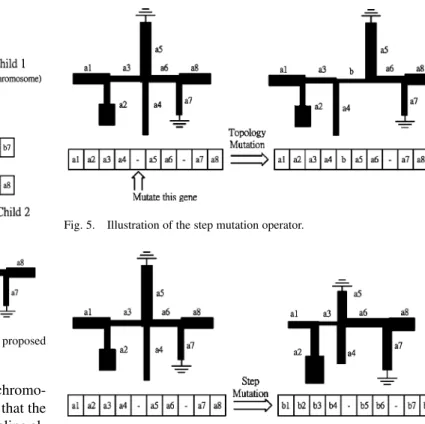
The proposed algorithm applies the one-point crossover method [10], as illustrated in Fig. 4. Unfortunately, such an operator may generate ill offspring. To avoid this, the con-straint testing in Fig. 2 is performed on the offspring. Step-and topology-mutation operators are both applied to produce offspring. The step-mutation operator [19] keeps the circuit topology and merely changes the electrical parameters in a chromosome, as shown in Fig. 5. The new electrical parameter in a chromosome is defined as
(9) where is the original electrical parameter and is a random variable in uniform distribution with a value from 1 to 1. The variable is interpreted as a mutation step size whose initial value is specified as 0.3. The step size of the next generation is adaptive according to the successful rate of the step mutations in this generation. To introduce more circuit topologies into a solution pool, we create the topology-mutation operator, which randomly selects one gene in a chromosome to change the cir-cuit topology, as well as the corresponding parameters, as shown in Fig. 6. Similar to the crossover operator, the offspring should meet the constraints. The probability to execute two mutation operators is equal in the beginning of the algorithm. However, the topology-mutation operator is disabled when the successful rate of this operator is less than 5% in five recent generations.
When the evolution count reaches the maximum value or one of the fitness value of a chromosome in a solution pool gets in the target fitness value, the algorithm terminates. Here, we
Fig. 5. Illustration of the step mutation operator.
Fig. 6. Illustration of the topology mutation operator.
specify the target fitness value as zero. In the generation evo-lution process, evaluating the scattering parameters is the most time-consuming step.
III. DESIGNEXAMPLES
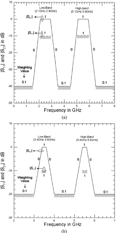
Here, two dual-band bandpass filters are designed and imple-mented to validate the proposed algorithm. The first filter is for IEEE 802.11 a/b/g WLAN systems and the designed specifica-tions are taken as
Return losses within 2.1–2.9 and 5.1–5.9 GHz 10 dB Rejections within dc: 1.5, 3.5–4.5, and 6.5–8.0 GHz 40 dB.
This filter possesses a sharp cutoff in the passbands and very good rejection in the stopbands. It covers all industrial–scien-tific–medical (ISM) and Unlicensed National Information Infra-structure (U-NII) bands. The specifications of the second filter are given as
Return losses within 3.4–3.6 and 5.4–5.6 GHz 10 dB Rejections within 2.0–3.0, 4.0–5.0, and 6.0–7.0 GHz 20 dB.
Differing from [17], whose rejections are merely required to be larger than 15 dB within 2.4–2.6 and 4.4–4.6 GHz, the above specifications aim at obtaining a dual-band bandpass filter with a sharper cutoff in the passbands and better rejection in the stop-bands.
The desired scattering parameters of the design examples ac-cording the forgoing specifications are described by piecewise-linear functions in Fig. 7, where the weighting value of each linear region is also depicted. For a sampling point within the shading portions in this figure, the score of the point is set to zero if the evaluated value is smaller than the desired value.
Fig. 7. Desired frequency responses of the examples. (a) Example 1. (b) Example 2.
The weighting values are carefully specified to obtain better fre-quency responses.
Two filters were fabricated on an RO4003 substrate with thickness mm and relative dielectric constant . Due to the tolerance of the fabrication, the min-imum width is limited to 0.2 mm, which corresponds to a microstrip line with a characteristic impedance of 110 . Meanwhile, to lower the junction discontinuity effects, the maximum line width is chosen to be 2 mm, which corresponds to a microstrip line with a characteristic impedance of 40 . To avoid coupling between adjacent stubs, the minimum electrical lengths of the TL and CTL are chosen to be 30 . Table II sum-marizes the upper and lower limits of the electrical parameters
TABLE II
UPPER ANDLOWERLIMITS OF THEELECTRICAL PARAMETERS IN THEDESIGNEXAMPLES
TABLE III
PARAMETERSETTINGS IN THETWOEXAMPLES
TABLE IV
ELECTRICAL ANDPHYSICALPARAMETERS OF THEFIRSTEXAMPLE
used in the two examples. The parameter settings for the two examples are then listed in Table III. Note that the constraints of the overall width of the circuit are loose since the shunt stubs can be bent to achieve compact design.
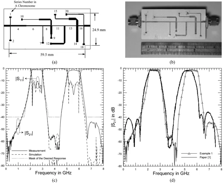
In the first example, the best chromosome after 300 gener-ations consists of four Empty elements, six thru transmission lines, and ten stubs. The achieved electrical parameters are then converted to a physical circuit. Table IV lists the electrical and physical parameters. The scattering parameters of the filter in-cluding the junction discontinuities are simulated again by the commercial circuit simulator ADS. To count the discontinuity effects and fringing capacitances, several physical parameters are slightly adjusted with the help of the commercial software. The layout, photography, and scattering parameters are shown
Fig. 8. First example. (a) Layout. (b) Photography. (c) Comparison between the simulated and measured scattering parameters. (d) Comparison of the measured jS j of the first example with that of the filter in [1].
in Fig. 8. As seen in Fig. 8(a), the small patches at the end of the stubs are for a grounding via and the long stubs are bent to reduce the overall width of the circuit. Referring to Fig. 8(c), the return losses are larger than 10 dB and the insertion losses are smaller than 2.6 dB from 2.14 to 2.96 and 5.14 to 6.06 GHz. In addition, the rejections are greater than 40 dB from dc to 1.31, 3.38 to 4.52, and 6.58 to 8.0 GHz. The 3-dB fractional band-width of the low- and high-band is 35% and 17%, respectively. In Fig. 8(d), the out-off-band rejection characteristics of the pro-posed filter are better than those of the filter in [1] because, in our design, the desired response in the out-of-band is required to be larger than 40 dB.
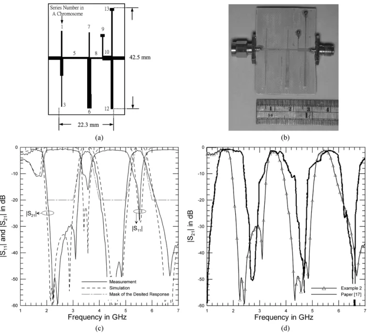
In the second example, after 300 generations, there are five
Empty elements, three thru transmission lines, and seven stubs
in the best chromosome. Table V lists the electrical and phys-ical parameters of the filter. Fig. 9(a) and (b) then shows the layout and photograph. Referring to Fig. 9(c), the return losses are larger than 10 dB and the insertion losses are smaller than 2.5 dB from 3.37 to 3.64 and 5.27 to 5.62 GHz. The rejec-tions are greater than 20 dB from 2.03 to 3.20, 4.04 to 5.0, and 6.13 to 7.0 GHz. The 3-dB fractional bandwidth of the low- and
TABLE V
ELECTRICAL ANDPHYSICALPARAMETERS OF THESECONDEXAMPLE
high-band is 9.9% and 7.9%, respectively. As seen in Fig. 9(d), it shows that the cutoff in the passbands and rejection in the stop-bands are better than that of the filter in [17]. Table VI compares
Fig. 9. Second example. (a) Layout. (b) Photography. (c) Comparison between the simulated and measured scattering parameters. (d) Comparison of the measured jS j of the second example with that of the filter in [17].
TABLE VI
COMPARISON OF THESIZES INTHISSTUDYWITHTHOSE OF THEFILTERS IN[1]AND[17]
the sizes of the circuits in this study with those of the filters in [1] and [17]. It reveals that the sizes of the proposed filters are nearly half as small as those of the filters presented before. All the works are completed on a personal computer with a 2.4-GHz microprocessor. The computing time of the two examples is 6 and 3 min, respectively.
IV. CONCLUSIONS
An optimization scheme based on hybrid-coded GA tech-niques has been presented to design compact and high-perfor-mance dual-band bandpass filters. This scheme is capable of simultaneously searching appropriate circuit topology and the corresponding electrical parameters with dual-band character-istic. Two filters have been designed and implemented to val-idate the proposed algorithm and both filters have manifested fairly good frequency responses and compact sizes. Future work will be in introducing new simple networks such as lumped
RLC elements, as well as active devices to the proposed
rep-resentation scheme for describing general passive and active microwave circuits. The proposed algorithm will then be ex-tended to synthesize more microwave circuits like broad-band matching networks and broad-band amplifiers.
APPENDIX A
Algorithm for Checking the Circuit Topology Represented by a Chromosome
Step 1) Remove all Empty genes in a chromo-some and regenerate a new set of structures
.
Step 2) Set .
Step 3) If , return an error message. Step 4) If , go to step 5. Otherwise set
and go to Step 6).
Step 5) If Type , return an error message.
Otherwise set .
Step 6) If , go to next step. Otherwise go to Step 3).
Step 7) Set and .
Step 8) If Type or , set
and return an error message if .
Step 9) If Type and , set .
Step 10) If Type and , set .
Set . If , terminate. Otherwise go to Step 8).
APPENDIX B
Algorithm for Evaluating Scattering Parameters of a Chromosome
Step 1) Remove all Empty genes in a chromo-some and regenerate a new set of structures
.
Step 2) Set and .
Step 3) For , if , go to Step
5).
Step 4) Evaluate where . Go to Step
6).
Step 5) Evaluate , , and where ,
, and
. Set .
Step 6) Set and . If , go to Step
7). Otherwise go to Step 3).
Step 7) Evaluate where .
In the above algorithms, denotes the number of non-Empty genes in a chromosome, returns an integer representing the circuit topology of structure ,
returns an integer representing the connection method of structure , evaluates the matrix of structure and
returns the matrix, evaluates the matrix
of structure and returns the matrix, converts the matrix to an matrix and returns the
Matrix, converts the matrix to an
matrix and returns the Matrix.
ACKNOWLEDGMENT
The circuits were fabricated and measured at the National Chiao Tung University, Hsinchu, Taiwan, R.O.C. The authors wish to express their sincere gratitude to Prof. R.-B. Hwang, and Prof. E. Y. Chang, both of the National Chiao Tung University,
for generously providing facilities for the experiments. More-over, the authors are indebted to Prof. J.-D. Tseng, National Chin-Yi Institute of Technology, Taichung County, R.O.C., for valuable ideas about the hairpin structure. The authors further wish to express their gratitude to Prof. T.-G. Ma, National Taiwan University of Science and Technology, Taipei, Taiwan, R.O.C., for reading this paper’s manuscript and making a number of valuable comments and T.-C. Pu, National Chiao Tung University, and P.-H. Deng, National Taiwan University, Taipei, Taiwan, R.O.C., for the helpful discussions.
REFERENCES
[1] L.-C. Tsai and C.-W. Hsue, “Dual-band bandpass filters using equal-length coupled-serial-shunted lines andZ-transforms technique,” IEEE
Trans. Microw. Theory Tech., vol. 52, no. 4, pp. 1111–1117, Apr. 2004.
[2] K. Wada, Y. Yamamoto, and O. Hashimoto, “Design of bandpass filters with a function to control the number of the attenuation pole,” IEICE
Trans. Electron., vol. E.85-C, no. 3, pp. 578–585, Mar. 2002.
[3] K. Wada, K. Nakagawa, O. Hashimoto, and H. Harada, “Technique for improving out-of-band characteristics of planar microwave filters using tapped resonators,” IEICE Trans. Electron., vol. E85-C, no. 2, pp. 391–399, Feb. 2002.
[4] K. Wada and O. Hashimoto, “Fundamentals of open-ended resonators and their application to microwave filters,” IEICE Trans. Electron., vol. E83-C, no. 11, pp. 1763–1775, Nov. 2000.
[5] J. W. Bandler, R. M. Biernacki, S. H. Chen, D. G. Swanson, and S. Ye, “Microstrip filter design using direct EM field simulation,” IEEE Trans.
Microw. Theory Tech., vol. 42, no. 7, pp. 1353–1359, Jul. 1994.
[6] J. W. Bandler, A. S. Mohamed, M. H. Baka, K. Madsen, and J. Son-dergaard, “EM-based optimization exploiting partial space mapping and exact sensitivities,” IEEE Trans. Microw. Theory Tech., vol. 50, no. 12, pp. 2741–2750, Dec. 2002.
[7] J. W. Bandler, Q. S. Cheng, N. K. Nikolova, and M. A. Ismail, “Implicit space mapping optimization exploiting preassigned parameters,” IEEE
Trans. Microw. Theory Tech., vol. 52, no. 1, pp. 378–385, Jan. 2004.
[8] J. E. Rayas-Sànchez, “EM-based optimization of microwave circuits using artificial neural networks: The state-of-the-art,” IEEE Trans.
Mi-crow. Theory Tech., vol. 52, no. 1, pp. 420–435, Jan. 2004.
[9] M.-H. Hsu and J.-F. Huang, “Annealing algorithm applied in optimum design of 2.4 GHz and 5.2 GHz dual-wideband microstrip line filters,”
IEICE Trans. Electron., vol. E88-C, no. 1, pp. 47–56, Jan. 2005.
[10] D. E. Goldberg, Genetic Algorithms in Search Optimization and
Ma-chine Learning. Reading, MA: Addison-Wesley, 1989.
[11] M. Gen and R. Cheng, Genetic Algorithms and Engineering
Optimiza-tion. New York: Wiley, 2000, ch. 3.
[12] Y. Ruhmat-Samii and E. Michielssen, Electromagnetic Optimization by
Genetic Algorithms. New York: Wiley, 1999.
[13] H. Choo and H. Ling, “Design of broad-band and dual-band microstrip antennas on a high-dielectric substrate using genetic algorithm,” Proc.
Inst. Elect. Eng.—Microwave Antennas Propag., vol. 50, pp. 137–142,
Jun. 2003.
[14] S. Chakravarty, R. Mittra, and N. R. Williams, “Application of a micro-genetic algorithm (MGA) to the design of broad-band microwave ab-sorbers using multiple frequency selective surface screens buried in di-electrics,” IEEE Trans. Antennas Propag., vol. 50, no. 3, pp. 284–296, Mar. 2002.
[15] P. L. Wener, R. Mittra, and D. H. Werner, “Extraction of SPICE-type equivalent circuits microwave components and discontinuities using the genetic algorithm optimization technique,” IEEE Trans. Adv. Packag., vol. 23, no. 1, pp. 55–61, Feb. 2000.
[16] S. F. Peik and Y. L. Chow, “Genetic algorithms applied to microwave circuit optimization,” in Proc. Asia–Pacific Microwave Conf., 1997, pp. 857–860.
[17] T. Nishino and T. Itoh, “Evolutionary generation of microwave line seg-ment circuits by genetic algorithms,” IEEE Trans. Microw. Theory Tech., vol. 50, no. 9, pp. 2048–2055, Sep. 2002.
[18] , “Evolutionary generation of 3-D line-segment circuits with a broadside-coupled multiconductor transmission-line model,” IEEE
Trans. Microw. Theory Tech., vol. 51, no. 10, pp. 2045–2054, Oct. 2003.
[19] D. M. Pozar, Microwave Engineering. New York: Wiley, 1998, ch. 8. [20] L.-H. Hsieh and K. Chang, “Slow-wave bandpass filters using ring or stepped-impedance hairpin resonators,” IEEE Trans. Microw. Theory
[21] , “Compact low-pass filters using microstrip stepped-impedance hairpin resonators,” IEEE Trans. Microw. Theory Tech., vol. 51, no. 1, pp. 193–199, Jan. 2003.
[22] , “Compact, low insertion-loss, sharp-rejection, and wide-band mi-crostrip bandpass filters,” IEEE Trans. Microw. Theory Tech., vol. 51, no. 4, pp. 1241–1246, Apr. 2003.
[23] A. E. Eiben, R. Hinterding, and R. Zbigniew, “Parameter control in evolutionary algorithm,” IEEE Trans. Evol. Comput., vol. 3, no. 2, pp. 124–141, Jul. 1999.
Ming-Iu Lai (S’04) was born in Kaohsiung, Taiwan, R.O.C., in 1976. He received the B.S.E.E. degree from National Taiwan University of Science and Technology, Taipei, Taiwan, R.O.C., in 1998, the M.S.E.E. degree from National Taiwan University, Taipei, Taiwan, R.O.C., in 2000, and is currently working toward the Ph.D. degree at National Taiwan University.
From 2001 to 2002, he was with the ZyXEL Communication Corporation, Hsinchu, Taiwan, R.O.C., where he was involved with signal integrity (SI) and electromagnetic interference (EMI) analyses. From 2002 to 2004, he was with the SynComm Communication Corporation, Hsinchu, Taiwan, R.O.C., and then joined the Applied Electromagnetic Research Laboratory, Microelectronics and Information System Research Center, National Chiao Tung University, Hsinchu, Taiwan, R.O.C., where he was involved with the designs of beam-steering antennas and high-frequency flip-chip packages. His current research interest includes two-dimensional/three-dimensional (2-D/3-D) microwave circuits design automation, grid computing techniques, and GAs for electromagnetic optimization designs, and time-domain numerical electromagnetics.
Shyh-Kang Jeng (M’86–SM’98) received the B.S.E.E. and Ph.D. degrees from National Taiwan University, Taipei, Taiwan, R.O.C., in 1979 and 1983, respectively.
In 1981, he joined the faculty of the Department of Electrical Engineering, National Taiwan Univer-sity, where he is currently a Professor. From 1985 to 1993, he was with the University of Illinois at Ur-bana-Champaign, as a Visiting Research Associate Professor and a Visiting Research Professor. In 1999, he was with the Center for Computer Research in Music and Acoustics, Stanford University, Stanford, CA, for six months. His research interest includes numerical electromagnetics, UWB wireless systems, music signal processing, music information retrieval, intelligent agent applica-tions, and electromagnetic scattering analysis.