高功函數矽化鉺金屬閘極之高溫穩定氮氧化鉿鑭P型金氧半場效電晶體研究
58
0
0
全文
(2) 高功函數矽化鉺金屬閘極之高溫穩定氮氧化鉿鑭P型 金氧半場效電晶體研究 The Research of High-Temperature Stable HfLaON p-MOSFETs With High-Work-Function Ir3Si Gate 研 究 生:周坤億 指導教授:荊鳳德. Student: Kun-I Chou. 博士. Advisor: Dr. Albert Chin. 國立交通大學 電子工程學系. 電子研究所碩士班. 碩士論文 A Thesis Submitted to Department of Electronics Engineering & Institute of Electronics College of Electrical and Computer Engineering National Chiao Tung University in Partial Fulfillment of the Requirements for the Degree of Master in Electronics Engineering. June 2008 HsinChu, Taiwan, Republic of China 中華民國九十七年六月.
(3) 高功函數矽化鉺金屬閘極之高溫穩定氮氧 化鉿鑭P型金氧半場效電晶體研究 學生: 周坤億. 指導教授: 荊鳳德 博士 國立交通大學. 電子工程學系電子研究所. 摘要 本論文研究高溫穩定矽化鉺金屬閘極之氮氧化鉿鑭 P 型金氧半場效電晶體元 件,此等效氧化層厚度為 1.6 奈米的元件在平帶電壓上一伏時有著 1.8×10⁻⁵A/cm2 的低漏電流,並且擁有高達 5.08 電子伏特的高功函數和 84cm2.S 的高移動率。 此閘極優先的 P 型金氧半場效電晶體製程是利用自我對準的離子布植技術和 1000℃快速高溫退火的方式來製作,而這些方法都相容於現在大尺寸製程整合的 生產線。. I.
(4) The Research of High-Temperature Stable HfLaON p-MOSFETs With High-Work-Function Ir3Si Gate Student: Kun-I Chou. Advisor: Dr. Albert Chin. Department of Electronics Engineering & Institute of Electronics Nation Chiao Tung University. Abstract We research a novel 1000℃ stable HfLaON p-MOSFET with Ir3Si gate. Low leakage current of 1.8 × 10⁻⁵ A/cm2 at 1 V above flat-band voltage, good effective work function of 5.08 eV, and high mobility of 84 cm2/V.s are simultaneously obtained at 1.6 nm equivalent oxide thickness. This gate-first p-MOSFET process with self-aligned ion implant and 1000 ℃ rapid thermal annealing is fully compatible to current very large scale integration fabrication lines.. II.
(5) 誌. 謝. 本論文得以完成,首先要感謝我的指導老師 荊鳳德 教 授,在兩年的碩士研究生涯裡,給予我豐富的指導與照顧, 不論是研究上與生活裡都讓我在這兩年裡獲得許多的收穫。 我還要感謝建宏學長、明峰學長、存甫學長與存護學長 他們在研究上與學業上給我的幫助,讓我得以順利完成碩士 研究。也要感謝維邦、冠霖、俊哲、思麟以及實驗室大家, 因為有你們的陪伴與支持,讓我度過愉快又充實的兩年。 最後,我要對我的父母獻上最高的敬意與謝意,感謝父 母對我的栽培、支持與鼓勵,以及家人的陪伴,才讓我有機 會能接觸這一切並且完成我的學業與研究。. III.
(6) Contents Abstract (in Chinese)…………………….…..………………………………I Abstract (in English)……………………..….……………………….……...II Acknowledgement……….……………..…….……..………………….……III Contents……………………………………………...…………………….…….IV Figure Captions………………………………………………………………..V Chapter 1 Introduction 1.1 Motivation to study high-k dielectrics……………………………….1 1.2 Motivation to study metal gate ………………………………………3 1.3 Introduction of this work……………………………………………..5. Chapter 2 Experimental Steps and Measurement 2.1 Fabrication of MOSFET……………………………………………12 2.2 The measurement of MOS capacitors…………………..…………..14. Chapter 3 Result and Discussion………………………..……….23 Chapter 4 Conclusion………………………………………………43 References……………………………………………………………………….44 Vita…………………………………………………………………………………48. IV.
(7) Figure Captions Chapter 1 Introduction Fig. 1-1 The evolution of MOS technology requirement……………………..………7 Fig. 1-2 The band offset of popular high-materials……………………………………8 Fig. 1-3 Bond enthalpy for M-O, M-N and M-C in the Periodic Table for thermal stability prediction, with M-O>M-N>M-C in general. The bond enthalpy peaked at La, Hf and Ta……………………………...………………………9 Fig. 1-4 Energy band diagram to show the increasing |Vt| in both n- and p-MOS…..10 Fig. 1-5 The schematic HfO2 bond diagram…………………………...…………….11. Chapter 2 Experimental Steps and Measurement Fig. 2-1 The RCA clean steps………………………………………………………..15 Fig. 2-2 Silicon substrate…………………………………………………..…………16 Fig. 2-3 RCA Clean………………………………………………………….……….16 Fig. 2-4. Deposited HfLaO dielectric……………………………………………….17. Fig. 2-5 NH3 plasma surface nitridation on HfLaO………………………………..17 Fig. 2-6. Deposition 5-nm amorphous-Si……………………………….…………..18. Fig. 2-7. Deposition 20-nm Ir…………………………………..…………………..18. Fig. 2-8 Formation of Ir3Si………………………………..…………………………19 V.
(8) Fig. 2-9 Deposition TaN capping layer to prevent ion……………………………….19 Fig. 2-10 Photoresist and Lithography……………………………………...………..20 Fig. 2-11 RIE etching……………………………………………………...…………20 Fig. 2-12 Self-aligned B+ implantation………………………………………..……..21 Fig. 2-13 source-drain doping activation at 1000℃ RTA for 5s……………….……22. Chapter 3 Result and Discussion Fig. 3-1 Grazing incident XRD spectra of HfLaO after different RTA annealing..…27 Fig. 3-2 Grazing incident XRD spectra of HfLaON with NH3 plasma after different RTA annealing. In contrast to the HfLaO case, the HfLaON stays amorphous state after 1000oC RTA………………………………………………..…..28 Fig. 3-3 XPS spectra of HfLaON after 1000℃ RTA. The existence of Hf, La, O, and N are clearly seen………………………………………………………..…29 Fig. 3-4 AES profile of Ir3Si/HfLaON/n-Si MOS structure after 1000℃ RTA. The Ir3Si accumulated toward HfLaON interface is found to un-pin the Fermi-level………………………………………………………….………30 Fig. 3-5 The comparison of gate leakage current density for MOS devices with SiO2 and HfLaON gate dielectrics…………………………………………….....31 Fig. 3-6 C-V characteristics of IrxSi/HfLaON, Ir/HfSiON, and Al/1000℃ -annealed-HfLaON capacitors measured under accumulation. The device VI.
(9) area is 100 μm×100 μm……………………………………………………..32 Fig. 3-7 J-V characteristics of IrxSi/HfLaON, Ir/HfSiON, and Al/1000℃-annealed-HfLaON capacitors measured under accumulation. The device area is 100 μm×100 μm……………………………………………..33 Fig. 3-8 TEM image of TaN/HfLaON/Si after 1000℃ RTA. Good interface property is observed with very thin interfacial layer……………………………...….34 Fig. 3-9 The dielectric constant of HfLaON and HfO2 at different RTA temperatures………………………………………………………………….………35 Fig. 3-10 XRD profiles of Ir3Si/HfLaON structure…………………………...……..36 Fig. 3-11 The Id-Vd characteristics of Ir3Si/HfLaON p-MOSFETs. The gate length is 4 μm…………………………………………………………………………37 Fig. 3-12 The hole mobility as a function of gate electric field of Ir3Si/HfLaON p-MOSFETs…………………………...…………………………………..38 Fig. 3-13 The accumulative failure vs. time-to-breakdown of HfLaON PMOS after 1000℃ RTA…………………………………..…………………………..39 Fig. 3-14 The maximum 10-year operation voltage plot from MTTF-tBD plot in Figure 3-13. Large extrapolated voltage of 2.6 V is obtained for 10 years operation…………………………………………………………………..40 Fig. 3-15 The ΔVt shift of IrxSi/HfLaON p-MOSFETs stressed at 85℃ and 10 VII.
(10) MV/cm for 1 hour…………………………………………………………41 Table 3-1 The table summarizes the comparison among various metal-gate/ high-κ CMOS………………………..…………………………………………42. VIII.
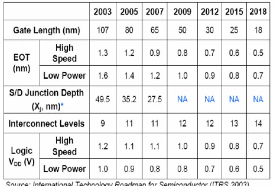
(11) Chapter 1 Introduction 1.1 Motivation to study high-k dielectrics With the improvement of the semiconductor processing technology, the scaling trend of MOSFETs devices will produce the large gate leakage current due to thinner gate oxide [1]-[2]. The MOSFETs exhibit significant leakage current more than 1 A/cm2 when the thickness of ultra-thin silicon gate oxide (SiO2) is less than 2 nm. The gate leakage current through the gate oxide increases significantly because the direct tunneling is the primary conduction mechanism in down-scaling CMOS technologies. To reduce the leakage current related higher power consumption in highly integrated circuit and overcome the physical thickness limitation of silicon dioxide, the conventional SiO2 will be replaced with high dielectric constant (high-κ) materials as the gate dielectrics beyond the 0.1 μm technology node [3]-[8]. Therefore, the engineering of high-κ gate dielectrics have attracted great attention and played an important role for VLSI. Although high-κ materials often exhibit smaller bandgap and higher defect density than conventional silicon dioxide, using the high-κ gate dielectric can efficiently increase the physical thickness in the same effective oxide thickness (EOT) that shows lower leakage characteristics than silicon dioxide by several orders without the reduction of capacitance density [4]-[7]. Recently, some 1.
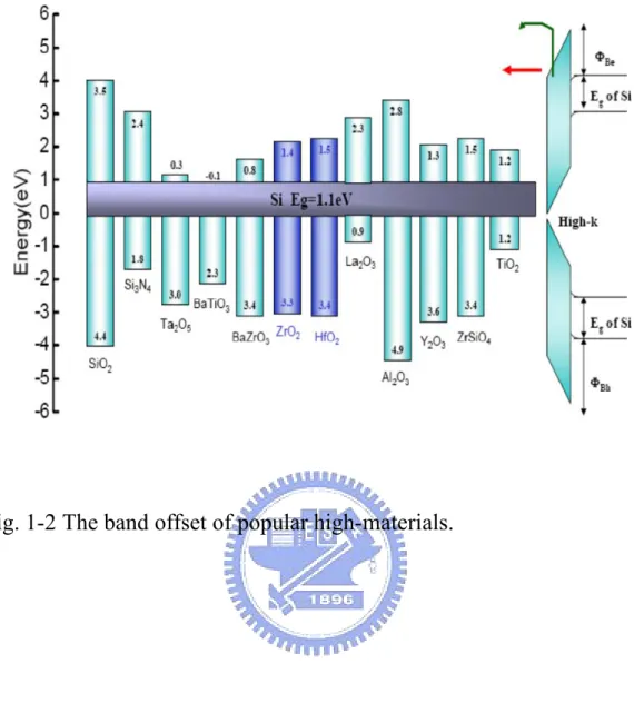
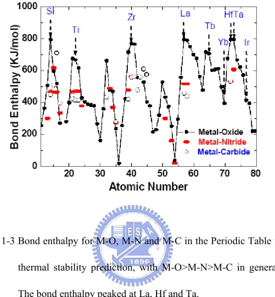
(12) high-κ materials have been widely studied and successfully intergraded in advanced MOSFETs or semiconductor devices, such as DRAMs or Flash memory and RF metal-insulator-metal (MIM) capacitors [9]-[10]. According to the ITRS (International Technology Roadmap for Semiconductor) [11] ,the suitable gate dielectrics must have value more than 8 for 50-70 nm technology nodes and that must be more than 15 when the technology dimension less than 50 nm. Figure 1-1 shows the evolution of CMOS technology requirements. Oxy-nitrides (SiOxNy) have been introduced to extend the use of SiO2 in production but eventually it has to be replaced by a high-κ material, such as Ta2O5, TiO2, HfO2, ZrO2, Al2O3, La2O3 or mixtures of them or metal-oxide-silicates of the mentioned compounds. However, most metal oxides will have the characteristics of crystallization at elevated temperature which cause devices generate non-uniform leakage distribution and give large statistical variation for nanometer devices across the chip. Therefore, replacement gate strategies have been proposed to prevent crystallization and deleterious effects of mass along grain boundaries. Figure 1-2 shows the summaries of the κ value and band offset for popular high-Κ!dielectric candidates. To predict the M-N thermal stability, in Figure 1-3 we show the bond enthalpy for various metal/dielectric combinations. In general the bond strength is that M-O> M-N> M-C.. 2.
(13) 1.2 Motivation to study metal gate As traditional poly-silicon (poly-Si) gated metal-oxide semiconductor field effect transistors (MOSFETs) scale down, the additional series capacitance due to poly-Si depletion becomes an increasingly large fraction of the total gate capacitance. Besides, diffusion of boron penetrates from the poly-Si gate will also degrade the performance of the transistors. To overcome these problems, using metal gate electrodes will be a practical way to eliminate poly gate depletion and boron penetration. In addition, metal gates also show the potential of reduced sheet resistance. Metal electrodes with suitable work functions and sufficient physical and electrical stability are being investigated to address these problems. In addition, thermal stability of the effective metal electrode and metal diffusion are also important considerations. Recently, lots of metal or metal-nitride materials have been widely researched and successfully intergraded in advanced CMOSFET’s, such as TiN, TaN, Pt, Mo and Ir. Tantalum (Ta) has a work-function close to n+ poly-Si. Tantalum nitride (TaN) is quite stable (to maintain thermal stability up to a 1000℃ RTA) because the activation energy of metal and nitrogen is relatively low. Tantalum is bonded tightly within nitride and no obvious diffuse was observed in fabricated devices. However, TaN gate on high-κ HfO2 shows a significant shift of flat band voltage (VFB) toward the mid-gap of Si due to the interface reaction between the TaN and HfO2 at the high temperature. This is 3.
(14) called the “Fermi-level pinning effect.” Therefore, the Fermi-level pinning effect needs to be avoided by selecting suitable metal gate and high-κ materials for advanced MOSFETs. Therefore, metal-gate/high-κ CMOSFETs show undesired high threshold voltages (Vt), which is opposite to the VLSI scaling trend. The increasing |Vt| in both metal-gate/high-k n- and p-MOS may be due to the interface dipole and charged defects formed by MN-MO reaction or [poly-Si]-MO reaction at high temperature, which altered the band diagram in Figure 1-4. Fermi level pinning of poly-Si and metal electrodes on HfO2 has been investigated. From Figure 1-5 the schematic HfO2 bond diagram, the metal accumulation at HfO2 surface may screen the surface dipole and un-bonded defect states, to reduce Fermi-level pinning. Furthermore, it has been shown that dosing surfaces with intra-layers can modify the interface dipole and band alignment, a phenomenon exploited in the fabrication of MOS gas sensors. The work functions (Φm) of metal shown in Figure 1-6 play an important role for metal-gate/high-κ CMOSFETs. The preferred work function of the metals are ~5.2 eV for p-MOSFETs and ~4.1 eV for n-MOSFETs. Recently, lots of metal or metal-nitride materials have been widely researched and successfully intergraded in advanced CMOSFETs, such as TiN, TaN, Pt, Mo and Ir. However, it has been found that thermal annealing of the metal gates at temperatures above 900℃ results in. 4.
(15) mid-gap values for almost all metal gate candidates. Therefore, the Fermi-level pinning effect needs to be avoided by selecting suitable metal gate and high-κ materials for advanced CMOS technologies.. 1.3 Introduce of this work According to the International Technology Roadmap for Semiconductors, the metal-gate/high-κ is the required technology for the future generation complementary MOSFETs to reduce the undesired large gate leakage current and continue the gate oxide scaling [12-22]. Currently, the HfSiON is a promising candidate beyond SiON with merits of high-κ value, low gate leakage current, and similar amorphous structure after 1000℃ rapid thermal annealing (RTA) for self-aligned process. However, the lack of a high-work-function gate for HfSiON p-MOSFETs is the challenge since only Ir (5.27 eV) and Pt (5.65 eV) in the periodic table [19] have the needed work function larger than the target 5.2 eV. The other problem of HfSiON is the relative lower κ of 10–14 that causes limited scaling capability. In this letter, we developed the high temperature stable Ir3Si/HfLaON p-MOSFET to address the aforementioned issues. The novel HfLaON dielectric can preserve the amorphous structure after 1000 ◦C RTA and is similar to HfSiON but with significantly higher κ value. Using high work- function Ir3Si gate electrode [19], [20], the p-MOSFETs show good device integrity of low leakage current of 1.8 × 10⁻⁵ A/cm2 at 1 V above flat-band voltage 5.
(16) Vfb, high effective work function φm-eff of 5.08 eV, high hole mobility of 84 cm2/V · s, and good 1000℃ RTA thermal stability at equivalent oxide thickness (EOT) of 1.6 nm. These results are compatible with or better than the best reported metal gate/high-κ p-MOSFETs [12-18].. 6.
(17) Fig. 1-1 The evolution of MOS technology requirement.. 7.
(18) Fig. 1-2 The band offset of popular high-materials.. 8.
(19) Fig. 1-3 Bond enthalpy for M-O, M-N and M-C in the Periodic Table for thermal stability prediction, with M-O>M-N>M-C in general . The bond enthalpy peaked at La, Hf and Ta.. 9.
(20) Fig. 1-4 Energy band diagram to show the increasing |Vt| in both n- and p-MOS.. 10.
(21) Fig. 1-5 The schematic HfO2 bond diagram.. 11.
(22) Chapter 2 Experimental Steps and Measurement 2.1 Fabrication of MOSFET Standard N-type Si wafers with resistivity 1~10 Ω-cm (1015-1016 cm-3 doping level) were used in this study, and following RCA clean processes. The detail steps of RCA clean is shows in Fig. 2-1. After standard RCA clean, the HfLaO was deposited on N-type Si wafers by PVD and post deposition anneal (PDA). The HfLaON was formed by applying NH3 plasma surface nitridation on HfLaO. Then 5 nm amorphous Si and 20 nm Ir was subsequently deposited on HfLaON and RTA annealed at 400~1000℃ for 30~5 sec to form the MOS capacitors. For comparison, Ir/HfSiON devices were also fabricated, where the HfSiON was formed by atomic layer deposition (ALD) of HfSiO and followed by surface plasma nitridation. The low temperature deposited Al gate on 1000℃ RTA-annealed HfLaON capacitors were also formed for φm-eff reference. For p-MOSFETs, additional thick TaN capping layer is added on Ir/Si/HfLaON to prevent subsequent ion implantation penetration, where the IrxSi gate was formed during RTA. After patterning, self-aligned B+ implantation was applied at 25 KeV and source-drain doping was activated at 1000℃ RTA for 5 sec.. 12.
(23) The fabricated p-MOSFETs were characterized by C-V and I-V measurements, and the processes of MOSFET is shown in Fig. 2-1 ~ Fig. 2-13.. 13.
(24) 2.2 The measurement of MOS capacitors To investigate the electrical characteristics of devices, we measured the Ig-Vg curves for gate leakage current by using HP 4156C semiconductor parameter analyzer. Besides, HP4284A precision LCR meter was used to evaluate the gate capacitance and the conductance ranging from 100 kHz to 1 MHz.. 14.
(25) A. DI water rinse, 5 min. B. H2SO4 : H2O2 = 3:1, (10 min, 75~85℃) C. DI water rinse, 5 min. D. HF : H2O = 1:100 E. DI water rinse, 5 min. F. NH4OH : H2O2 : H2O = 1:4:20 (SC1), (10 min,75~85℃) G. DI water rinse, 5 min. H. HCl : H2O2: H2O = 1:1:6 (SC2), (10min, 75~85℃) I. DI water rinse, 5 min. J. HF : H2O = 1:100 K. DI water rinse. L. Spinner Fig.2-1 The RCA clean steps.. 15.
(26) N-type Si Fig. 2-2 Silicon substrate.. RCA Clean. N-type Si Fig.2-3 RCA Clean.. 16.
(27) HfLaO N-type Si. Fig.2-4 Deposited HfLaO dielectric.. NH3 plasma surface nitridation. HfLaON. HfLaO. N-type Si Fig.2-5 NH3 plasma surface nitridation on HfLaO.. 17.
(28) Deposition 5-nm amorphous-Si. HfLaON. HfLaO. N-type Si Fig.2-6 Deposition 5-nm amorphous-Si.. Deposition 20-nm Ir. Ir(200Å) HfLaON. HfLaO. N-type Si. Fig.2-7 Deposition 20-nm Ir. 18.
(29) RTA annealed at 400-1000℃ for 30-5 s. Ir3Si HfLaON. HfLaO. N-type Si. Fig.2-8 Formation of Ir3Si.. Deposition TaN. TaN Ir3Si HfLaON. HfLaO. N-type Si. Fig.2-9 Deposition TaN capping layer to prevent ion implantation penetration. 19.
(30) Photoresist TaN Ir3Si HfLaON. HfLaO. N-type Si Fig.2-10 Photoresist and Lithography.. RIE. Photoresist TaN Ir3Si HfLaON. HfLaO. N-type Si Fig.2-11 RIE etching.. 20.
(31) B+. Photoresist. B+. TaN Ir3Si HfLaON. HfLaO. N-type Si. Fig. 2-12 Self-aligned B+ implantation.. 21. B+.
(32) RTA TaN Ir3Si HfLaON. HfLaO. B+. N-type Si. B+. Fig. 2-13 source-drain doping activation at 1000℃ RTA for 5s. 22.
(33) Chapter 3 Result and Discussion Figures 3-1 and 3-2 show the XRD comparison of HfLaO and HfLaON with different RTA temperature. After 1000℃ RTA, strong undesired crystallization in HfLaO is clear measured, but in sharp contrast, the HfLaON still preserves the amorphous state. The existence of Hf, La, O and N in HfLaON is confirmed by XPS in Figure 3-3. The metal-gate Ir3Si on HfLaON are further analyzed by AES. As shown in Figure 3-4, such good device characteristic is due to the nitridation on thick high-κ that prevents Ir3Si metal diffusion through HfLaON. The high φm-eff is due to the Ir3Si accumulated toward HfLaON interface to un-pin the Fermi-level. Figure 3-5 shows the J-EOT plot, where much improved leakage current than SiO2 is obtained at 1.7 nm EOT. In addition, high κ of 20 is still preserved even after 1000oC RTA and much better than HfO2. Figures 3-6 and 3-7 show the C-V and J-V characteristics respectively, for different RTA temperature annealed IrxSi/HfLaON capacitors. The Ir/HfSiON and Al/1000oC-annealed-HfLaON devices are also shown for comparison. An increasing Vfb trend with increasing RTA annealing temperature is measured, which is attributed to IrxSi reaction toward high-κ interface [19]-[20]. The Ir on HfSiON shows the highest Vfb, but the capacitor failed after 1000℃ RTA. In contrast, the IrxSi/HfLaON have good 1000℃ thermal stability by converting 23.
(34) the Ir to IrxSi by inserting ~5 nm amorphous Si; however, the better thermal stability is traded off the slightly lower Vfb. From the C-V shift to control Al gate on 1000℃ RTA annealed HfLaON, the extracted φm-eff of Ir3Si/HfLaON is 5.08 eV. Here the Al gated capacitor was chosen as a reference because low temperature deposited pure metal has little Fermi-level pinning on high-κ dielectric [15]-[16], [19]-[20] and the same 1000℃ RTA ensures the similar oxide charge in HfLaON to Ir3Si-gated devices. The using Al control gate is to avoid oxide charge difference on thickness introduced by nitrogen-plasma treatment and process variation. Anyway, the fixed charge density should be small from the good mobility shown following. The merit of using HfLaON rather than HfSiON is clearly seen by the orders of magnitude leakage current improvement. Very low leakage current of 1.8×10⁻⁵ A/cm2 at 1V above Vfb are measured in IrxSi/HfLaON at 1.6 nm EOT. Such low leakage current is attributed the high κ value of 20 and amorphous structure after 1000℃ RTA from cross-sectional TEM measurement in Figure 3-8. The decreasing stretch of C-V curves with increasing RTA temperature suggests the improving oxide quality annealing out the defects at high temperatures. Therefore, high φm-eff of 5.08 eV, low gate leakage current of 1.8×10⁻⁵ A/cm2 (Vfb+1V) and good thermal stability of 1000℃ RTA can be achieved at the same time in IrxSi/HfLaON MOS capacitors at 1.6 nm EOT. The decreasing capacitance density with increasing RTA temperature is related to slight. 24.
(35) decreasing κ value reduction shown in Figure 3-9, but the amount of reduction is significantly less than HfO2. We have further used the X-Ray Diffraction (XRD) measurements to characterize the IrxSi. As shown in Figure 3-10, the Ir-rich IrxSi with x=3 was formed with distinct 2θ angle to residual Ir peak. The x=3 in IrxSi was determined by comparing the measured peak XRD pattern with published data . The amorphous structure of HfLaON was also confirmed by glazing angle XRD measurements even after 1000℃ RTA .Figure 3-11 shows the transistor Id-Vd characteristics as a function of Vg-Vt for 1000℃ RTA annealed Ir3Si/HfLaON p-MOSFETs and good transistor characteristics are obtained. Here the Vt is -0.1 V as obtained from the linear Id-Vg plot and consistent with the large φm-eff of 5.08 eV from C-V curves. Figure 3-12 shows the hole mobility plot as a function of gate electric field of Ir3Si/HfLaON p-MOSFETs. High hole mobility of 84 and 63 cm2/V-s are obtained at peak value and 1 MV/cm effective field for Ir3Si/HfLaON p-MOSFETs, respectively. This result is comparable with the reported HfSiON p-MOSFET in the literature [12]-[18] with advantages of process compatible to current VLSI line. In Figures 3-13 and 3-14, a large 2.6 V operation voltage for 10-years is obtained from the tBD plot. Further reliability study is from the BTI shown in Figure 3-15, where <20 mV shift are measured for CMOS at 10 MV/cm stress and 85℃ for 1 hr.. 25.
(36) Table 3-1 summarizes the comparison among various metal-gate/ high-κ CMOS.. 26.
(37) Fig. 3-1 Grazing incident XRD spectra of HfLaO after different RTA annealing.. 27.
(38) Fig. 3-2. Grazing incident XRD spectra of HfLaON with NH3 plasma after different RTA annealing. In contrast to the HfLaO case, the HfLaON stays amorphous state after 1000oC RTA. 28.
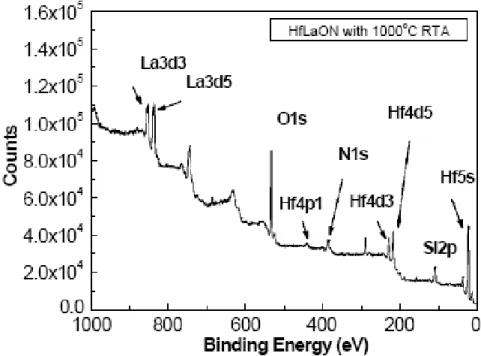
(39) Fig. 3-3 XPS spectra of HfLaON after 1000℃ RTA. The existence of Hf, La, O, and N are clearly seen.. 29.
(40) Fig. 3-4 AES profile of Ir3Si/HfLaON/n-Si MOS structure after 1000℃ RTA. The Ir3Si accumulated toward HfLaON interface is found to un-pin the Fermi-level.. 30.
(41) Fig. 3-5 The comparison of gate leakage current density for MOS devices with SiO2 and HfLaON gate dielectrics.. 31.
(42) Fig. 3-6 C-V characteristics of IrxSi/HfLaON, Ir/HfSiON, and Al/1000℃ -annealed-HfLaON capacitors measured under accumulation. The device area is 100 μm×100 μm.. 32.
(43) Fig. 3-7 J-V characteristics of IrxSi/HfLaON, Ir/HfSiON, and Al/1000℃ -annealed-HfLaON capacitors measured under accumulation. The device area is 100 μm×100 μm.. 33.
(44) Fig. 3-8 TEM image of TaN/HfLaON/Si after 1000℃ RTA. Good interface property is observed with very thin interfacial layer.. 34.
(45) Fig. 3-9 The dielectric constant of HfLaON and HfO2 at different RTA temperatures.. 35.
(46) Fig. 3-10 XRD profiles of Ir3Si/HfLaON structure.. 36.
(47) Fig. 3-11 The Id-Vd characteristics of Ir3Si/HfLaON p-MOSFETs. The gate length is 4 μm. 37.
(48) Fig. 3-12. The hole mobility as a function of gate electric field of Ir3Si/HfLaON p-MOSFETs.. 38.
(49) Fig. 3-13 The accumulative failure vs. time-to-breakdown of HfLaON PMOS after 1000℃ RTA.. 39.
(50) Fig. 3-14 The maximum 10-year operation voltage plot from MTTF-tBD plot in Figure 3-13. Large extrapolated voltage of 2.6 V is obtained for 10 years operation.. 40.
(51) Fig. 3-15 The ΔVt shift of IrxSi/HfLaON p-MOSFETs stressed at 85℃ and 10 MV/cm for 1 hour.. 41.
(52) Table 3-1 The table summarizes the comparison among various metal-gate/ high-κ CMOS.. 42.
(53) Chapter 4 Conclusion We report novel 1000℃-stable HfLaON p-MOSFET with Ir3Si gate. Low leakage current of 1.8×10⁻⁵ A/cm2 at 1 V above flat band voltage, good effective work function of 5.08 eV and high mobility of 84 cm2/Vs are simultaneously obtained at 1.6 nm equivalent-oxide thickness. This gate-first p-MOSFET process with self-aligned ion implant and 1000℃ RTA is fully compatible to current VLSI fabrication lines.. 43.
(54) Reference [1] Wang Bin, J. S. Suehle, E. M. Vogel and J. B. Bernstein, “Time-dependent breakdown of ultra-thin SiO2 gate dielectrics under pulsed biased stress,” IEEE Electron Device Lett. 22, pp. 224-226, 2001. [2] J. H. Stathis, A. Vayshenker, P. R. Varekamp, E. Y. Wu, C. Montrose, J. McKenna, D. J. DiMaria, L. -K. Han, E. Cartier, R. A. Wachnik and B. P. Linder, “Breakdown measurements of ultra-thin SiO2 at low voltage,” in IEDM Tech. Dig., pp. 94-95, 2000. [3] M. Koyama, K. Suguro, M. Yoshiki, Y. Kamimuta, M. Koike, M. Ohse, C. Hongo and A. Nishiyama, “Thermally stable ultra-thin nitrogen incorporated ZrO2 gate dielectric prepared by low temperature oxidation of ZrN,” in IEDM Tech. Dig., pp. 20.3.1-20.3.4, 2001. [4] E. P. Gusev, D. A. Buchanan, E. Cartier, A. Kumar, D. DiMaria, S. Guha, A. Callegari, S. Zafar, P. C. Jamison, D. A. Neumayer, M. Copel, M. A. Gribelyuk, H. Okorn-Schmidt, C. D Emic, P. Kozlowski, K. Chan, N. Bojarczuk, L. -A. Ragnarsson and Rons, “Ultrathin high-Κ!gate stacks for advanced CMOS devices,” in IEDM Tech. Dig., pp. 20.1.1-20.1.4, 2001. [5] W. Zhu, T. P. Ma, T. Tamagawa, Y. Di, J. Kim, R. Carruthers, M. Gibson and T. Furukawa, “HfO2 and HfAlO for CMOS: thermal stability and current transport,” in IEDM Tech. Dig., pp. 20.4.1-20.4.4, 2001. [6] L. Kang, K. Onishi, Y. Jeon, Byoung Hun Lee, C. Kang, Wen-Jie Qi, R. Nieh, S. Gopalan, R Choi and J. C. Lee, “ MOSFET devices with polysilicon on single-layer HfO2 high-Κ!dielectrics,” in IEDM Tech. Dig., pp. 35-38, 2000. [7] Rino Choi, Chang Seok Kang, Byoung Hun Lee, K. Onishi, R. Nieh, S. Gopalan, E. Dharmarajan and J. C. Lee, “High-quality ultra-thin HfO2 gate dielectric MOSFETs with TaN electrode and nitridation surface preparation,” in IEDM Tech. Dig., pp. 15-16, 2001. 44.
(55) [8] Z. J. Luo, T. P. Ma, E. Cartier, M. Copel, T. Tamagawa and B. Halpern, “Ultra-thin ZrO2 (or silicate) with high thermal stability for CMOS gate applications,” in Symp. on VLSI Technology, pp. 135-136, 2001. [9] K. C. Chiang, C. H. Lai, Albert Chin, T. J. Wang, H. F. Chiu, J. R. Chen, S. P. McAlister, and C. C. Chi, “Very High-Density (23 fF/Μm2) RF MIM Capacitors Using high-Κ!TaTiO as the Dielectric,” IEEE Electron Device Lett. 26, no. 10, pp. 728-730, 2005. [10] K. C. Chiang, Albert Chin, C. H. Lai, W. J. Chen, C. F. Cheng, B. F. Hung, and C. C. Liao, “Very High Κ!and High Density TiTaO MIM Capacitors for Analog and RF applications,” Symp. on VLSI Technology, pp. 62-63, Japan, June 2005. [11] International Technology Roadmap for Semiconductor, 2004. [12] H.-H. Tseng, C. C. Capasso, J. K. Schaeffer, E. A. Hebert, P. J. Tobin, D. C. Gilmer,D. Triyoso, M. E. Ramón, S. Kalpat, E. Luckowski, W. J. Taylor, Y. Jeon, O. Adetutu,R. I. Hegde, R. Noble, M. Jahanbani, C. El Chemali, and B. E. White, “Improved short channel device characteristics with stress relieved pre-oxide (SRPO) and a novel tantalum carbon alloy metal gate/HfO2 stack,” in IEDM Tech. Dig., 2004, pp.821-824. [13] X. Yu, M. Yu and C. Zhu, “Advanced HfTaON/SiO2 gate stack with high mobility and low leakage current for low –standby-power application,” IEEE Electron Device Lett. Vol. 27, no. 6, 2006, pp. 498-501. [14] S. C. Song, Z. Zhang, C. Huffman, J. H. Sim, S. H. Bae, P. D. Kirsch, P. Majhi, R. Choi, N. Moumen, and B. H. Lee, “Highly manufacturable advanced gate-stack technology for sub-45-nm self-aligned gate-first CMOSFETs,” IEEE Trans. Electron Devices, vol. 53, no. 5, 2006, pp. 979-989.. 45.
(56) [15] T. Nabatame, M. Kadoshima, K. Iwamoto, N. Mise, S. Migita, M. Ohno, H. Ota, N.Yasuda, A. Ogawa, K. Tominaga, H. Satake, and A. Toriumi, “Partial silicides technology for tunable work function electrodes on high-Κ!gate dielectrics- fermi level pinning controlled PtSix for HfOx(N) pMOSFET,” in IEDM Tech. Dig., 2004, pp.83-86. [16] K. Takahashi, K. Manabe, T. Ikarashi, N. Ikarashi, T. Hase, T. Yoshihara, H. Watanabe, T. Tatsumi, and Y. Mochizuki, “Dual workfunction Ni-silicide/HfSiON gate stacks by phase-controlled full-silicidation (PC-FUSI) technique for 45nm-node LSTP and LOP devices,” in IEDM Tech. Dig., 2004, pp. 91-94.88 [17] P. F. Hsu, Y. T. Hou, F. Y. Yen, V. S. Chang, P. S. Lim, C. L. Hung, L.G. Yao, J. C.Jiang, H. J. Lin, J. M. Chiou, K. M. Yin, J. J. Lee, R. L. Hwang, Y. Jin, S. M. Chang, H. J. Tao, S. C. Chen, M. S. Liang, and T. P. Ma, “Advanced dual metal gateMOSFETs with high-Κ!dielectric for CMOS application,” in Symp. VLSI Tech. Dig.,2006, pp. 14-15. [18] H. Y. Yu, R. Singanamalla, K. Opsomer, E. Augendre, E. Simoen, J.A. Kittl, S. Kubicek, S. Severi, X.P. Shi, S. Brus, C. Zhao, J.F. de Marneffe, S. Locorotondo, D. Shamiryan, M. Van Dal, A. Veloso, A. Lauwers, M.Niwa, K. Maex, K. D. Meyer, P. Absi, M. Jurczak, and S. Biesemans, “Demonstration of Ni Fully GermanoSilicide as a pFET Gate Electrode Candidate on HfSiON,” in IEDM Tech. Dig., 2005, pp.653-656. [19] D. S. Yu, Albert Chin, C. H. Wu, M.-F. Li, C. Zhu, S. J. Wang, W. J. Yoo, B. F. Hung and S. P. McAlister, “Lanthanide and Ir-based dual metal-gate/HfAlON CMOS with large work-function difference,” in IEDM Tech. Dig., 2005, pp. 649-652. [20] C. H. Wu, D. S. Yu, Albert Chin, S. J. Wang, M.-F. Li, C. Zhu, B. F. Hung, and S. P.McAlister, “High work function IrxSi gates on HfAlON p-MOSFETs,” IEEE ElectronDevice Lett. 27, no. 2, 2006, pp. 90-92. [21] C. H. Wu, B. F. Hung, Albert Chin, S. J. Wang, F. Y. Yen, Y. T. Hou, Y. Jin, H. J. 46.
(57) Tao,S. C. Chen, and M. S. Liang, “HfAlON n-MOSFETs Incorporating Low Work Function Gate Using Ytterbium-Silicide,” in IEEE Electron Device Lett. vol. 27, no. 6, June 2006, pp. 454-456. [22] X. P. Wang, C. Shen, M.-F. Li, H. Y. Yu, Y. Sun, Y. P. Feng, A. Lim, H. W. Sik, A.Chin, Y. C. Yeo, P. Lo, and D. L. Kwong, “Dual metal gates with band-edge work functions on novel HfLaO high-κ gate dielectric,” in Symp. VLSI Tech. Dig., 2006, p.12-13.. 47.
(58) Vita 姓名:周坤億 性別:男 出生年月日:民國72年10月1日 籍貫:台灣省台北縣 住址:台北縣樹林市南園里7鄰佳園路三段101巷62弄61號 學歷:國立東華大學物理學系 (90年9月~95年1月) 國立交通大學電子研究所固態電子組 (95年9月入學). 論文題目: 高功函數矽化鉺金屬閘極之高溫穩定氮氧化鉿鑭P型金氧半場效電晶體研究 (The research of high-temperature Stable HfLaON p-MOSFETs with high-work-function Ir3Si gate). 48.
(59)
數據
+7

相關文件
①尼古丁 ②焦油 ③一氧化碳
在1980年代,非晶矽是唯一商業化的薄膜型太 陽能電池材料。非晶矽的優點在於對於可見光
Given a shift κ, if we want to compute the eigenvalue λ of A which is closest to κ, then we need to compute the eigenvalue δ of (11) such that |δ| is the smallest value of all of
雙極性接面電晶體(bipolar junction transistor, BJT) 場效電晶體(field effect transistor, FET).
The Knowledge Value Added theory provides a promising model for quantitative performance measurement of a CoP as long as the value-adding activities are identified with the quantified
Several methods that modulation effective work function to maintain p-type gate material is the direction of future research, sush as microwave annealing with plasma
Iwai , “A self-aligned emitter base NiSi electrode technology for advanced high-speed bipolar LSIs” , in IEEE Bipolar/BiCMOS Circuits and Technology Meeting , pp..
酸性氣體(二氧化硫、二氧化氮)可以飄浮到離源頭很遠的地
![HPSH [ 氧化數平衡反應式係數 ]](data:image/gif;base64,R0lGODlhAQABAIAAAP///wAAACH5BAEAAAAALAAAAAABAAEAAAICRAEAOw==)