Electromigration induced failure in SnAgt.sCuo.7 Solder Joints for
Flip
Chip Technology
Y-C Hsu, T-L Shao and Chih Chen Department of Material Science and Engineering
National Chiao Tung University Hsinchu, Taiwan 300 Email: vins(&”hinet.net Phone: 886-3-5712 121-55377
Abstract
Electromigration of SnAg&uo,7 solder was investigated in flip chip solder bump. An under-bump metallization (UBM) of CriCr-CuiCu tri-layer was deposited on the chip side and electroless CURriiiAu pad was deposited on the BT, board side. Electromigration damage was observed under the current density of 2 x IO‘ A/crnZ at 100
“C.
Voids were found at cathode side and crack was observed at solder/thin film UBM interface aRer current stressing, and the bump failed after 168-hour stressing. Copper atoms were found to move in the direction of elcctron flow. Intermetallic compounds of Cu-Sn and Ni-Cu-Sn were also observed to spread into the solder bump due to current stressing. \Introduction
Flip Chip technology has been used in electronics industry due to the higher packaging density (more I/Os), better performance, smaller device footprints, and lower packaging profile. This technology consist two basic steps, first solder bumps are deposited on the chips and reflowed, then the chips are flipped over, aligned to a substrate, and reflowed again [ 1][2]. Serious reliability issues like thermal-mechanical fatigue, heat dissipation and electromigration have received tremendous amount of attention in these solder bumps. Concerning electromigration problem, the number of inpulloutput pin counts will increase for the flip chip products in the near future, the bump pitch and the diameter of UBM decrease rapidly due to the small contact area of the solder bumps. For solder bumps in flip chip technology is approaching to 5 0 p m in diameter, if a solder bump was carry 0.2A electrical current, the current density will reach to 1O4Alcm2 and is large enough to cause electromigration damage, so the eletromigration in flip chip solder bumps needs to be investigated. For the recent studies
on
electromigration were mainly focus on eutectic SnPh solder [3]-[6]. Due to the environmental concern, Ph containing solders will he replaced by Pb-free solder. SnAg,.,Cuo., solder will be one of the most promising lead-free solders in microelectronic packaging industly. However, only a few researches have been studied on the solder humps of SnAg, ~Cuo.l[7]-[9].In this work, the electromigratoin of SnAgl.sCuo., flip chip structure has been studied under the current density of 2 x IO4 Ncm’ at 100 %. Current crowding and polarity
effect were examined in the solder bump. The failure was found to be at solder and thin film CriCr-CulCu tri-layer interface.
Experiment
The SnAgCu solder humps structure was stressed at
100°C of the current density of 2 x IO4 A/cm20n a hot plate
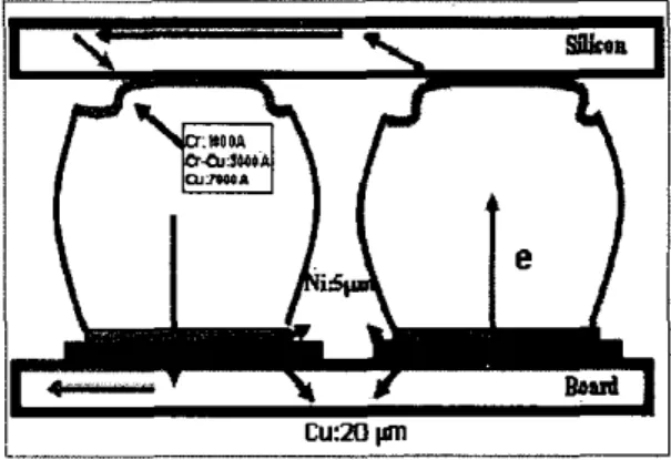
in atmospheric ambient. An under-bump metallization (UBM) of CriCr-CdCu tri-layer was deposited on the chip side and electroless CuMilAu pad was deposited on the BT board side. The solder bumps were formed by printing solder paste through a metal stencil and reflowed twice in a furnace. Then the package was filled with underfill. In order to observe the electromigration of the solder bumps under high current density, the solder bumps were cross sectioned first, then they were stressed at the current density of 2 x IO“ A i m 2 . Schematic diagram of the structure is shown in Fig. I .
IL
id
I
cu:m
ImFig. I Schematic diagram of sold bump structure Electromigration damage was examined by scanning electron microscope (SEM). Composition of intermetallic compound and migration of metal atoms were determined by using energy dispersive spectroscopy(EDS). Due to the Aluminum circuit design in the structure, electron flow is moved upward from the board side to the letl comer of the chip side, then downward from the left corner of the chip side to the hoard side as indicated by the arrows in Fig. 1. This will lead current crowding effect at these comers in the
solder bumps
Results and discussion
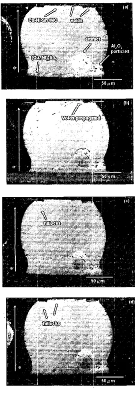
Fig. 2(a) through 2(e) illustrate the electromigration phenomenon in SnAg,.&uo7 solder hump before and after stressing for 20, 70, 110, 168 hours, respectively. Intermetallic compounds (Cu, Ni)& was observed at the interface of solder and Ni UBM interface and also in the solder. However it is only a few intermetallic compounds at the interface of solder and Cu UBM. This is attributed to the thickness of Cu at UBM. Cu may almost dissolve into the solder and react with Tin after reflowed.
The direction of the electron flow is from board side Ni UBM toward chip side. The original voids at solder and Cu thin film UBM interface can he observed in Fig. 2(a). Voids propagated as stressing time increased, and hillocks were observed at the left side of the UBM as shown in Fig. 2(h) through 2(d). At Ni thick film and solder interface, voids were only observed at the center of the interface after stressing as shown in Fig. (3). The solder bump was failed after 168 hours stressing, the surface sank and become very rough.
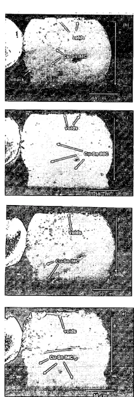
At Cu thin film and solder interface, hillocks and lump were observed. They are due to mass transport by the electron flow. Also the voids can he observed and propagated during current stressing. It is attributed that, in the solder hump, metal atoms were migrated with electron flow from the hoard side to the left comer of chip side, the more and more metal atoms were accumulated at the left upper comer, and mass transport by metal atoms induced voids concentration gradient at the solder and UBM interface, voids were pushed from the left side to the right side during electromigraton. Consequently voids propagated and became crack. Fig. 4(a) through 4(e) illustrate the electromigration phenomenon with opposite polarity before and after stressing of 20, 70, 110, 168 hours, respectively. The direction of electron flow now is from the chip side to the board side. Voids and hillocks were observed at cathode side and anode side, respectively. The voids were propagated as stressing time increased. The solder hump was failed after 168-hour stressing, the surface sank and become very rough.
Intermetallic compounds of Cu-Sn and Cu-Sn-Ni were observed to spread into the solder hump due to current stressing. Intermetallic compound found in the solder is not uniformly distributed, there were more compound particles on the right-hand. This is due to the current crowding effect, since electron flow is from the left comer
of
the chip side downward to the board side.Besides
intermetallic compounds of Cu-Sn and Cu-Sn-Ni were observed to accumulate at solder and UBM interface as shown in Fig. 4(e). Fig. 5(a) and 5(h) are the enlarged image of Fig. 4(e). The elemental EDS mapping and Cu accumulation were observed at the left side of the UBM clearly due to current stressing. However, in the solder hump which with opposite direction of electron flow, Cu-Sn and Cu-Sn-Ni intermetallic compound were not found to spread into the solder bump. This is due to that the opening of Ni UBM is larger than Cu UBM, which means that the current density of the Ni UBM is much lower thanof Cu UBM.
UBM side is more serious than that of Ni UBM.
Therefore, the electromigration damage at Cu
Fig. 2. Cross-sectional SEM images of the solder bump under the current density of 2 x
IO'
A/cmz at 100"C
(a) Ohr, (b) 20hrs, (c) 70hrs, (d) IlOhrs, and (e) 168hrsFig. 3 Cross-sectional SEM image of the solder bump after 168 h n stressing. Voids were observed at the middle of the interface.
Fig. 4 Cross-sectional SEM images of the solder bump under the current density of 2 x IO' A i m Z at 100 C (a) Ohr, (b) ZOhn, (c) 7Ohrs, (d) I IOhrs, and (e) 168hrs.
(a) (b)
c u
Fig. 5(a) enlarged image of Fig. 4(e), and (b)the elemental EDS mapping, dot mal ofCu element.
Conclusions
Electromigration induced failure in SnAg,.&b., solder joints was observed under the current density of 2 x
IO'
Alcm2at 100%. Voids were found at cathode side and crack was observed at solder/thin film UBM interface alter current stressing. Current crowding and polarity effect were examined. Copper atoms were found to move in the direction of the electron flow. Intermetallic compounds of Cu-Sn and Ni-Cu-Sn were also observed to spread into the solder bump due to current stressing. Bump failed after 168-hour stressing. .Acknowledgment
The financial support of this study is from National Science Council of Republic of China under NSC-91-22 16-E-009-032 Reference I . 2. 3. 4. 5. 6 . 7.
8.
9. ~~ ~~~I. H. Lau, Flip Chip Technology(McGraw-Hill, New York, 1996).
J . H. Lau and Shi-Wei Ricky Lee, Chip Scale Package(McCraw-Hill, New York, 1999).
C. Y. Liu, Chih Chen, and K. N. Tu, J. Appl. Phys. 88,
5703
(2000).T. Y. Lee and K. N. Tu, J. Appl. Phys. 89, 3189 (2001).
Kazuyuki Nakagawa, Shinji Bada, Masaki Watanabe, Hironori Matsushima, Kozo Harada, Eiji Hayashi, ECTC, lEEE Proceedings (2001)
J. D. Wu, P. J . Zheng, Kelly Lee, C. T. Chiu, and I. J . Lee, ECTC, IEEE Proceedings, 452 (2002).
S.
Y. Jang, J. Wolf, W. S . Kwon, K. W. Paik, ECTC, IEEE Proceedings, 1213 (2002).T. Y. Lee and K. N. Tu,
J.Appl. Phys. 90,4502 (2001). C. M. Chen and S. W. Chen, J. Appl. Phys. 90, 1208(2001).