國
立
交
通
大
學
多媒體工程研究所
碩 士 論 文
應用於超高速傳輸多天線系統(MIMO-OFDM)頻域上之高時脈誤
差容忍時間同步器
Frequency-Domain Timing Synchronizer with Wide Clock Offset Tolerance in
Very-High-Throughput MIMO-OFDM Systems
研 究 生:陳名瑜
指導教授:張立平 教授
應用於超高速傳輸多天線系統(MIMO-OFDM)頻域上之高時脈誤
差容忍時間同步器
Frequency-Domain Timing Synchronizer with Wide Clock Offset Tolerance in
Very-High-Throughput MIMO-OFDM Systems
研 究 生:陳名瑜 Student:Ming-Yu Chen
指導教授:張立平 Advisor:Li-Pin Chang
國 立 交 通 大 學
多 媒 體 工 程 研 究 所
碩 士 論 文
A ThesisSubmitted to Institute of MultimediaEngineering College of Computer Science
National Chiao Tung University in partial Fulfillment of the Requirements
for the Degree of Master
in
Computer and Information Science August 2009
Hsinchu, Taiwan, Republic of China
應用於超高速傳輸多天線系統(MIMO-OFDM)頻域上
之高時脈誤差容忍時間同步器
研究生:陳名瑜
指導教授:張立平 教授
國立交通大學多媒體工程研究所 碩士班
摘要
隨著無線通訊技術的快速發展,超高速傳輸系統已成為新一代無線通訊系統的發 展核心,然而高速傳輸需要更快的取樣頻率,這將使得「大量取樣頻率偏移」此問題 發生的機率增加,這將造成訊號嚴重的衰減。因此,本論文致力於研究在2048-FFT下 超高速多天線正交分頻多工系統中(MIMO OFDM),頻率域上的時間同步器,並以調節 取樣相位的方式補償取樣頻脈誤差,達到同步取樣的目的。 本論文所提出的演算法,主要應用在 IEEE 所制定的無線區域網路標準 IEEE 802.11n,藉由利用封包前端格式固定的preambles,針對其彼此間的相關性對取樣頻 率誤差作估計以及補償。此演算法中,總共使用六個preambles。在高斯雜訊及多路 徑 衰 減 的 情 形 下 , 以 封 包 錯 誤 率 (PER) 小 於 8% 為 標 準 , 效 能 可 以 達 到 容 忍 -30000~40000-ppm的時脈偏移影響。Frequency-Domain Timing Synchronizer with Wide Clock
Off-set Tolerance in Very-High-Throughput MIMO-OFDM Systems
Student: Ming-Yu Chen
Advisor: Dr. Li-Pin Chang
Institute of Multimedia Engineering College of Computer Science,
National Chiao Tung University
Abstract
Due to the explosive growth demand for wireless communication, the next-generation wireless communication systems are expected to provide high-speed and high-throughput. However, high-speed transmission needs high sampling rate, which would cause wide sam-pling clock offset. Based on phase adjustment, this work investigates a frequency-domain timing synchronizer to perform coherent sampling for 2048-FFT Multiple-Input Mul-tiple-Output (MIMO) Orthogonal Frequency Division Multiplexing (OFDM) timing recov-ery.
In the proposed algorithm, we use a multiphase all-digital clock management (ADCM) which can generate more than 32 phases over GHz without phase-locked or delay-locked loops to adjust sampling phases and utilize the correlation between short preambles to es-timation the sampling phase error. It can perform the sampling clock synchronization effi-ciently and quickly. Performance evaluation indicates that the proposed timing synchroniz-er can tolsynchroniz-erate -30000 ~ 40000ppm sampling clock offsets with 0.2db SNR losses at 8% PER in frequency-selective fading. Hence, this scheme involves a little overhead to ensure fast recovery and wide offset tolerance for OFDM packet transmissions.
Acknowledgements
This thesis describes research work I performed in the Integration System and Intellec-tual Property (ISIP) Lab during my graduate studies at National Chiao Tung University (NCTU). This work would not have been possible without the support of many people. I would like to express my most sincere gratitude to all those who have made this possible.
First and foremost I would like to thank my advisors Dr. Termg-Ying Hsu and Dr. Li-Pin Chang for the advice, guidance, and funding he has provided me with. I feel honored by being able to work with him.
I am very grateful to You-Hsien Lin, Ming-Fu Sun, Wei-Chi Lai, Ta-Young Yuan, and those members of ISIP Lab for their support and suggestions.
Finally, and most importantly, I want to thank my parents for their unconditional love and support they provide me with. It means a lot to me.
MING-YU CHEN June 2009
Contents
page
中文摘要 ……….i 英文摘要 ………....ii 誌謝 ………iii 目錄 ………iv 圖目錄 ………vi 表目錄 ………vii CHAPTER1 INTRODUCTION ……….………..1CHAPTER2 SYSTEM ASSUMPTIONS ………..………4
2.1 IEEE 802.11n Physical Layer Specification ………...4
2.1.1 Transmitter ……….………...4
2.1.2 Receiver ………..5
2.1.3 Basic MIMO PPDU Format ……….5
2.2 Channel model ……….………...6
2.2.1 Additive White Gaussian Noise …….………...6
2.2.2 Multipath ...……….………....7
2.2.3 Sampling Clock Offset ...………....8
2.3 Problem statement …..……….………...9
CHAPTER3 FD- TIMING SYNCHRONIZER …...10
3.1 Sampling clock offset estimation ………...10
3.2 Sampling phase acquisition ………....15
3.3 Combine sampling phase acquisition and SCO estimation …...19
3.4 Compensation ………...20
CHAPTER4 SIMULATION ………….………..22
4.1 Simulation platform ……….………...22
CHAPTER5 HARDWARE IMPLEMENTATION ………..25 CHAPTER6 CONCLUSIONS AND FUTURE WORKS ……….27 REFERENCES ………...………...28
List of Figures
page
Figure 1 Block diagram of simplified wireless communication systems .…………...1
Figure 2 Block diagram of FD-Timing Synchronizer for OFDM timing recovery ...2
Figure 3 IEEE 802.11n transmitter data path ……..………..……...4
Figure 4 IEEE 802.11n receiver data path …………..………...……..5
Figure 5 PPDU Format for NTX antennas ………….……….….……..…..5
Figure 6 OFDM training structure include of L-STF and L-LTF……....……...6
Figure 7 Block diagram of channel model ……….………...6
Figure 8 Block diagram of channel model ………..………7
Figure 9 Channel frequency response ………..………...8
Figure 10 Influence of SCO in time domain ………...………...……….…………8
Figure 11 The phase rotation on each subcarrier under SCO ………11
Figure 12 Block diagram of the SCO estimation algorithm ……...……….11
Figure 13 The differences of the phase rotation on two short preambles …………12
Figure 14 The differences of the phase rotation on two short preambles …..………14
Figure 15 Phase adjustment-based multiphase A/D sampling and timing detector...15
Figure 16 The state diagram of sampling phase acquisition ………...16
Figure 17 PDF of sampling phase error ………..……..18
Figure 18 Block-diagram of six preambles ………...19
Figure 19 PDF of sampling phase error ………..…..20
Figure 20 The state diagram of compensation ………..………...20
Figure 21 PDF of sampling phase error-2……….……….23
Figure 22 The system performance with 64-QAM ………..…….23
Figure 23 The root means square error of sampling phase ……….24
Figure 24 Offset tolerance with SNR=14-dB, 100-ns RMS delay spreading…..……24
Figure 25 Architecture of hardware implementation……...………25
List of Tables
page
TABLE I The state of the art ..………..………9
TABLE II The state of the art ……...…..……….………14
TABLEIII Decision criteria of eight regions…....…………..………...17
TABLE IV Simulation parameters ...…..…...…….………..22
TABLE V RMS of sampling phase error…...……….………23
TABLEVI Hardware specifications ……….…...……...………..26
TABLE VII Area report ……...………...……….………..26
TABLE VIII Summary of the measured EVM ………..27
CHAPTER 1
INTRODUCTION
With the explosive growth demand for wireless communications, the next-generation wireless communication systems are expected to provide ubiquitous, high-quality, high-speed, reliable, and spectrally-efficient. However, to achieve this objective, several technical challenges have to be overcome attempt to provide high-quality service in this dynamic environment.
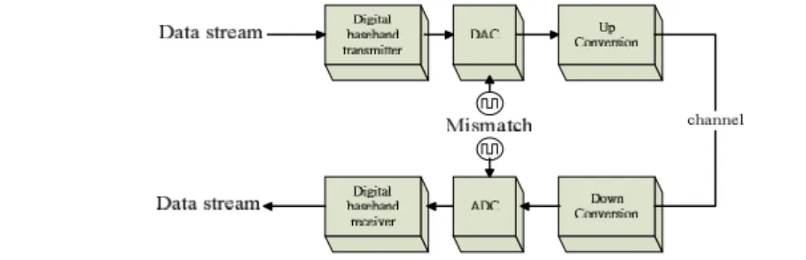
Orthogonal frequency-division multiplexing (OFDM) is a spectrally efficient signaling me-thod for communication over frequency-selective fading channels, which divides the given bandwidth into multiple orthogonal subcarriers. OFDM has been adopted as a core technology by many transmission systems, such as IEEE802.11a/g-based WLAN systems, digital audio broad-casting (DAB) and digital video broadbroad-casting terrestrial TV (DVB-T). Multiple-Input mul-tiple-output (MIMO) wireless systems with multiple antennas at both transmit and receive sides can be faster and more efficient than single-input single-output (SISO) systems. Unfortunately, OFDM systems are sensitive to imperfect synchronization and non-ideal front-end effects, lead-ing to serious degradations of system performance. The key impact is that the signal is not sampled at the optimum point, due to sampling clock offset (SCO) and sampling phase offset. A major origin of sampling clock offset is the mismatch of local oscillators between the transmitter and the receiver, as shown in Figure1. Furthermore, it may cause inter-symbol interference (ISI) and inter-carrier interference (ICI), because of the accumulation of sampling phase shift and the phase rotations of subcarrier in frequency domain. In order to avoid these problems, it is in most cases necessary to measure and compensate SCO and sampling phase offset.
A number of methods for sampling clock offset estimation have been proposed in the litera-ture. Most of them are based on frequency domain pilots on OFDM data symbols [1-4], and sev-eral methods utilize the long training field HT-LTFs of the preamble [5]. However, when SCO is wide, pilot-based timing recovery may cause performance degradation of preamble-based algo-rithm, due to those preambles which have been destroyed by SCO.
Fixed sampling with an interpolation filter [6-9] is a well-developed method, in which datum are sampled at the Nyquist or higher rate. Interpolation techniques are usually employed to re-cover analog-to-digital converters (A/D) sampling, high-order structures are needed to ensure accurate output [10-11]. The other timing recovery involves adaptive sampling (synchronized sampling) to make analog-to-digital converters (A/D) coherent. Since lower information loss corresponds to better performance, adaptive sampling (synchronized sampling) outperforms fixed sampling (non-synchronized sampling) [12-14]. The key of adaptive sampling is to adjust A/D clock accurately, efficiently and stably. Several mixed-mode schemes [15-19] have been devel-oped to control A/D sampling frequency. Instead of analog techniques, an all-digital phase-locked loop (ADPLL) with 8 uniform phases [20] has been realized to reduce power dissipation and im-plementation costs of MB-OFDM UWB systems. Yet, the large number of multiphase of ADPLL is hard to implement over several hundred MHz. Unlike other multiphase techniques, e.g., phase-locked loops (PLL), delay-locked loops (DLL) and analog circuits, a 2n-multiphase all-digital clock management (ADCM) [21] have been adopted, which is easy to produce multi-phase over GHz using an in-house digital cell library. Although its disadvantage is a non-uniform skew of clock phases (caused by rise time≠fall time) .
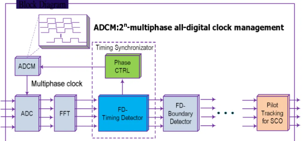
Based on phase adjustment, this work investigates a frequency domain timing synchronizer, which provides a wide offset tolerance in OFDM packet accesses, as shown in Figure 2. It uses the first six Legacy Short Training Sequences (L-STS) to estimation SCO and sampling phase offset. Furthermore, compensate sampling phase in time domain with the multiphase technique which are implemented by all-digital clock management (ADCM). The proposed algorithm is well-suited to new specifications discussed in IEEE 802.15.3c and IEEE 802.11 Very High Throughput working group (VHT WG).
The rest of this paper is organized as follows. In Chapter 2, a brief introduction states the system description and system model. Chapter 3 describes the proposed timing synchronizer for MIMO-OFDM. Chapter 4 shows and discusses the results. Conclusions are finally drawn in Chapter 5.
CHAPTER 2
System Assumptions
The simulation platform is MIMO-OFDM system. It is constructed according to the standard of IEEE. 802.11n and utilize FFT to implementation OFDM. In the section, there are three main blocks, i.e., IEEE802.11n specification, channel model, and problem state.
2.1 IEEE 802.11n Physical Layer Specification
2.1.1 Transmitter
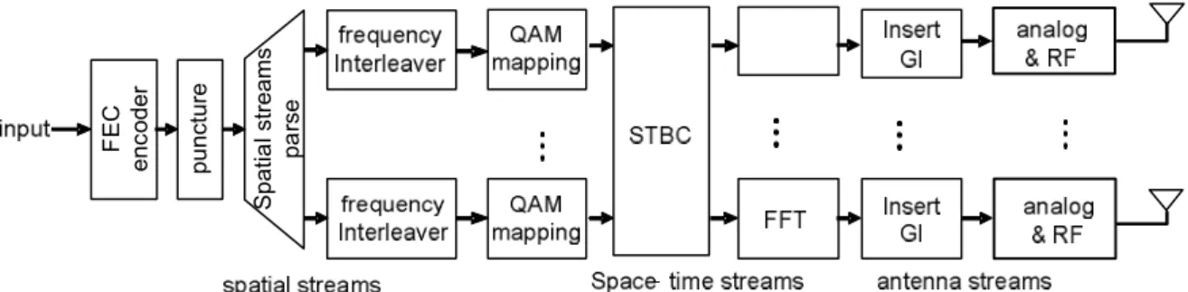
The IEEE 802.11n is known as multi-input-multi-output OFDM system (MIMO-OFDM), op-erating in both 2*2 and 4*4 and 8*8 antennas to transmit and receive data and support higher coding rate up to 5/6. Figure 3 shows transmitter data path. First use FEC encoder to encodes the source data. Then the bit stream is parsed into spatial streams, according to the number of trans-mit antennas. The interleaver provides a form of diversity to guard against localized corruption or bursts of errors. And then, the QAM mapping is used to modulate the bit stream. It supports BPSK, QPSK, 16 QAM, 64 QAM, 64 QAM or 256 QAM. After QAM mapping, the constella-tion points pass through Space Time Block Code (STBC) encoder. The STBC encoder spreads the constellation points of each spatial stream to any other spatial streams. IFFT is used to trans-fer signal from frequency domain to time domain. In 80MHz, there are 2048 frequency entries for each IFFT, or 2048 sub-carriers in each OFDM symbol, 1702 of them are data carriers, 142 of them are pilot carriers, other are null carriers. After Insert Guard Interval (GI), the signal is transmitted by RF. S p a ti a l s tr e a m s p a rs e p u n c tu re F E C e n c o d e r
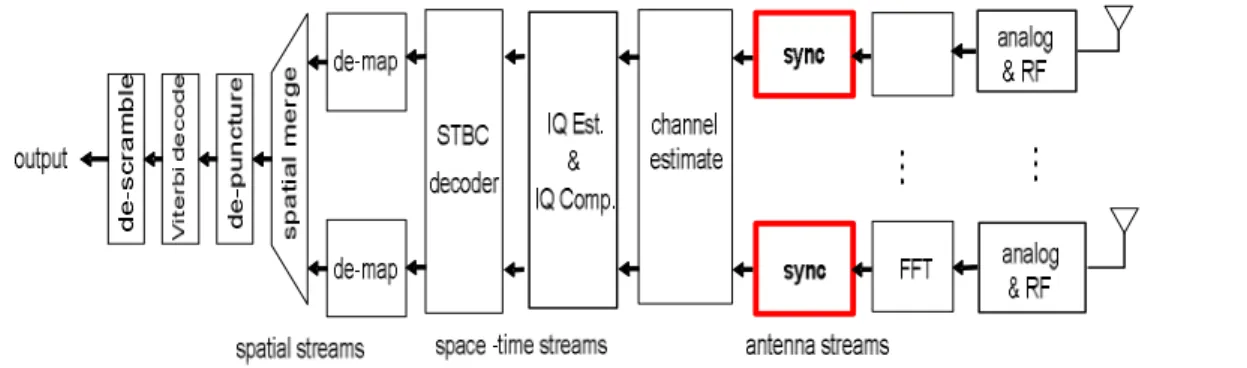
Figure 4: IEEE 802.11n receiver data path 2.1.2 Receiver
Figure 4 shows receiver data path. The signal is received from the RF. FFT is used to transfer received signal from time domain to frequency domain. Sync is used for synchronization, in-cluding to find when exactly the packet start, the OFDM symbol boundary and the best sample phase. Channel effect will be estimated and compensated by Equalizer. IQ mismatch is also taken under consideration. After all estimation and compensation, STBC decoder is used to com-bine four bit streams into original. Then the bit streams are de-map, de-interleaver and merge to single data stream. Finally, it is decoded by FEC which includes de-puncturing, Viterbi decoder and de-scrambler.
2.1.3 Basic MIMO PPDU Format
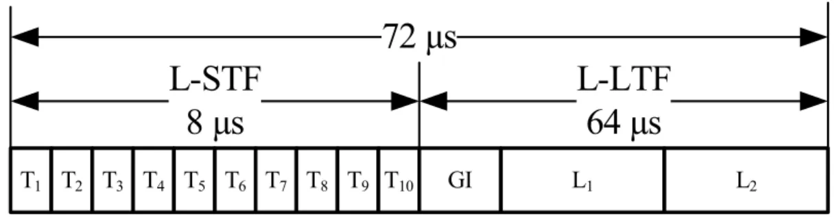
A PHY protocol data unit (PPDU) is defined to provide interoperability. Figure 5 shows the PPDU format for the basic MIMO mode. Each packet contains a header (ex. L-STF, L-LTF) for detection, channel estimation and synchronization purposes. For preventing unintentional beam-forming, insertion of the cyclic shifts (CSD) is applied to the preamble and signal fields. First part is the L-STF which can be used for signal detection, coarse acquisition …etc. The L-STF is formed by the repetition of ten L-STS of 64 samples each; these samples have correlation proper-ties. In this thesis, correlation techniques will be applicable for packet detection, symbol boun-dary detection, and timing synchronization. A detail data structure of L-STF is shown as Figure 6.
2.2 Channel Model
There are many imperfect effects during transmitted signals through channel, such as Addi-tive White Gaussian Noise (AWGN), sampling clock offset (SCO), multipath, and so on. The block diagram of channel model is shown in Fig. 7.
2.2.1 Additive White Gaussian Noise
Wideband Gaussian noise comes from many natural sources, such as the thermal vibrations of atoms in antennas, "black body" radiation from the earth and other warm objects, and from celes-tial sources such as the sun. The AWGN channel is a good model for many satellite and deep space communication links. On the other hand, it is not a good model for most terrestrial links because of multipath, terrain blocking, interference, etc. The signal distorted by AWGN can be derived as
( )
( )
( )
r t
s t
n t
(2.1)
wherer t
( )
is received signal,( )
s t
is transmitted signal,( )
n t
is AWGN. T1 T2 T3 T4 T5 T6 T7 T8 T9 T10 GI L1 L2L-STF
8 µs
L-LTF
64 µs
72 µs
Figure 6: OFDM training structure include of L-STF and L-LTF
TX
TX
Time invariance
multipath SCO AWGN
Figure 8: Block diagram of channel model 2.2.2 Multipath
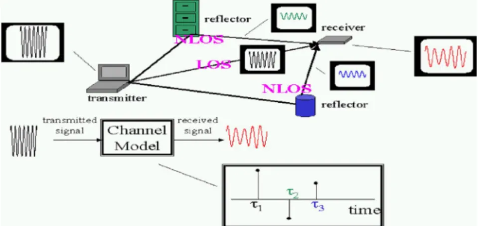
Because there are obstacles and reflectors in the wireless propagation channel, the transmit-ted signal arrivals at the receiver from various directions over a multiplicity of paths, as shown in Figure 8. Such a phenomenon is called multipath. It is an unpredictable set of reflections and/or direct waves each with its own degree of attenuation and delay. Multipath is usually described by two sorts:
a. Line-of-sight (LOS): the direct connection between transmitter and receiver. b. Non-line-of-sight (NLOS): the path arriving after reflection from reflectors.
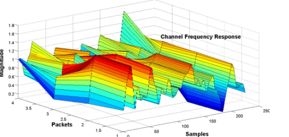
Multipath will cause amplitude and phase fluctuations, and time delay in the received signals. When the waves of multipath signals are out of phase, reduction of the signal strength at the re-ceiver can occur. One such type of reduction is called the multipath fading; the phenomenon is known as “Rayleigh fading” or “fast fading.” Besides, multiple reflections of the transmitted sig-nal may arrive at the receiver at different times; this can result in inter symbol interference (ISI) that the receiver cannot sort out. This time dispersion of the channel is called multipath delay spread which is an important parameter to access the performance capabilities of wireless sys-tems. For a reliable communication without using adaptive equalization or other anti-multipath techniques, the transmitted data rate should be much smaller than the inverse of the RMS delay spread. A representation of Rayleigh fading and a measured received power-delay profile are shown in Figure9.
Figure 9: Channel Frequency Response
)))
1
(
:
)
2
((
)
(
*
)
1
(
*
*
)
1
(
*
X
X
R
ion(
interpolat
nT
R
X
T
n
Y
T
n
X
preADC s s s
2.2.3 Sampling Clock Offset
The clock drift means the different between the sampling frequency of the digital to analog converter (DAC) and the analog to digital converter (ADC). Because of sampling frequency off-set, even if the initial sampling point is optimized, the following sampling points will still slowly shift with time. This model is using timing shift and cubic interpolation to cause the clock drift effect and its effect can be written as Eq. 2.
(2.2)
where RpreADC represents the ADC original output signal, δ represents SCO and to get R nT ( s)
signal by shift the ADC original output signal and interpolation the fractional part Y. Figure 10 shows the clock drift model effect. Initial can samples at optimum sampling points, then slightly incorrect sampling instants will cause the SNR degradation.
2.3 Problem Statement
Due to the explosive growth demand for wireless communication, the next-generation wire-less communication systems are expected to provide high-speed and high-throughput. However, high-speed transmission needs high sampling rate, which would cause wide sampling clock off-set.
In TABLE Ⅰ, it compares some methods of timing synchronization in the state of the art. In those methods, the largest tolerance of SCO is 675ppm, which is not large enough. The above mention has said that the wide clock offset tolerance is the core of the development for high-speed transmission. Hence, the thesis works on the wide clock offset in very high through-put MIMO OFDM systems.
TABLE I:
THE STATE OF THE ART
[1] [3] [21] [25]
System Type OFDM OFDM +4-QAM
MIMO-OFDM +64-QAM
OFDM +16-QAM
Method N/A Phase in Freq.
Non-PLL ADCM
(ADCM) Interpolator
Required Format Pilot Preamble Short Preambles Preamble
Tolerant Range 675 ppm 400ppm 400 ppm 100 ppm
CHAPTER 3
FD-Timing Synchronizer
Timing synchronization is one of the most important things in wireless OFDM systems. The duty of the synchronization is to help the receiver to get information correctly. There are symbol timing offset and sampling timing offset that constitutes timing synchronization errors. The ADC is the first stage of baseband, so it dominates the receiving signal to noise ratio (SNR). To get the highest input SNR, the ADC is hoped to sample at the eye open position where it has the maxi-mum signal power. In this thesis, we will focus on the study of sampling timing offset.
In this section, a frequency-domain synchronizer is proposed for sampling timing offset. The synchronizer contains two parts: sampling phase offset and sampling clock offset. The 8*8 2048-FFT MIMO-OFDM system with complicated channel model is aimed.
3.1 Sampling clock offset estimation
Sampling clock offset means the different between the sampling frequency of the digital to analog converter (DAC) and the analog to digital converter (ADC). Because of the sampling fre-quency offset, even if the initial sampling point is optimized, the following sampling points will still slowly with time. In Eq. 3.1, the normalized sampling error is defined as r t
t
T T
T
where
t
T
and T are the transmitter and receiver sampling period, and the sampling timing offset, rt
n T , increase with index n.
[ ]
(
r) = ( (1
) ) = (
t t t)
r n
r nT
r n
T
r nT
n T
(3.1)
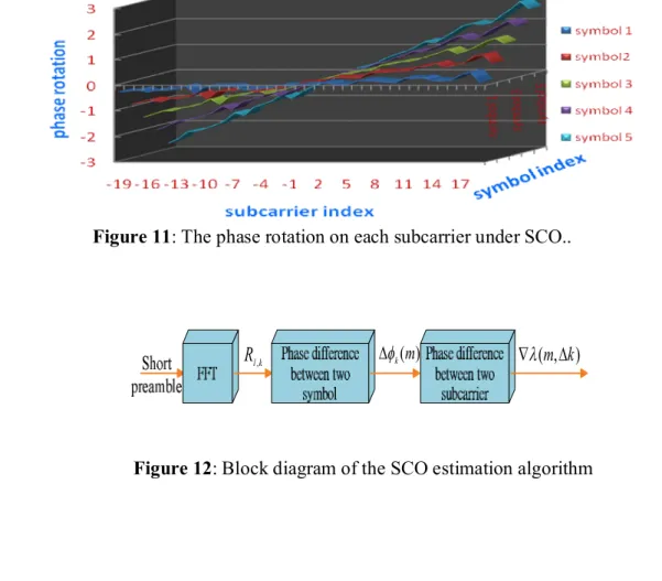
After DFT, the effect due to the clock offset is the phase rotate, as shown in Eq. 3.2 and Fig-ure 11.
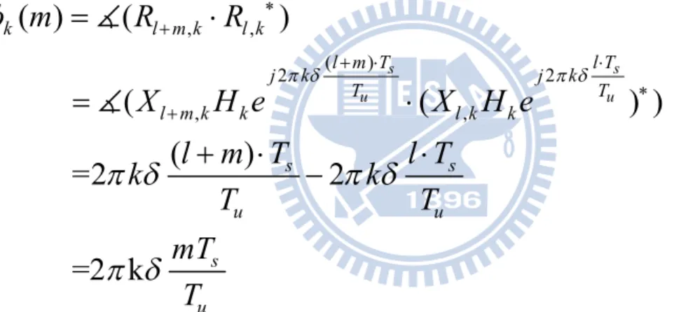
2 , , , , 2 ,
H
s u s u lT j k T l k l k l k l k lT j k T l k
R
X
e
W
e
(3.2)
In the equation, l is the symbol index, k is the subcarrier index, Ts is the total symbol du-ration, T is the useful data portion and u H is the channel frequency response. In the case of l k,slow varying channels,
1, 2,
l k l k
H H . The term
l k, causes the received data rotation. The rota-tion angle is depends on both the subcarrier index k and the symbol indexl. Figure 11 shows the phase rotation occurred between different symbols and subcarriers. It is obvious that phase rotations increase with the increasing of symbol index and subcarrier index. When subcarrier in-dex is negative, the phase rotation is also negative.Figure 11: The phase rotation on each subcarrier under SCO..
, l k
R k( )m ( ,m k )
Figure 13: The difference of the phase rotation on two short preambles
This algorithm of sampling clock offset estimation is based on the non-HT short training preamble, utilizing the correlation between the two same short preambles. Figure 12 shows the block diagram of the SCO estimation algorithm. Basing on Eq. 3.3, the value of the phase rota-tion
l k, is proportional to subcarrier index and symbol index. First, we translate shortpream-ble to frequency domain by N-FFT, where N is the number of samples in one short preampream-ble, as shown in Eq. 3.3. 1 2 , 0
[(
1)
]
nk N j N l k nR
r l
N
n e
(3.3)
Next on, compute the difference, k( )m , between the two phases on the th
k subcarrier in
the th
l and (lm)thshort preambles, as shown in Eq. 3.4.
, , ( ) 2 2 , ,
( )
(
)
(
(
) )
(
)
=2
2
=2 k
s s u u k l m k l k l m T l T j k j k T T l m k k l k k s s u u s um
R
R
X
H e
X
H e
l
m T
l T
k
k
T
T
mT
T
(3.4)
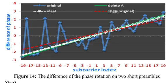
According to Eq. 3.4, a linear relationship is reported between k( )m and k, hence we want to get the slope of the linear function. However, it may be destroyed in the presence of low SNR and multipath fading channel, as shown in Figure 13. In order to decrease the effect, we use some mechanisms to improve the accuracy of slope estimation.
The key construct of those mechanisms is to get rid of seriouslydestroyed data following three steps:
Step 1:
According to the subcarrier index, divide
k( )
m
into two groups, C1
k( ) | m k0} and
2 k( )| 0}
C m k , where C1 means the negative index group of subcarrier and C2 means the positive one. The elements in the same group need to be with the same sign, so we use majority rule to delete the fewer elements, such as point A shown in Figure 13.
Step2:
Compute the phase difference between the different subcarriers, ( ,m k),and ( ,1)m is the slope of the line in Figure14 .
1 2 1 2
( ,
)
( )
( )
=2
2
=2
k
k k s s u u s um
k
m
m
mT
mT
k
k
T
T
mT
T
(3.5)
However, Figure 14 shows that the line composed by phase difference and subcarrier index is not perfect with the influences of AWGN and multipath, so we use the least square algorithm to get the optimal slope. According to the linear algebra theory, if x is the least square solution of the systemAxb, the x can be gotten using Eq. 3.6.
1(
)
T T T TAx
b
A Ax
A b
x
A A
A b
(3.6)
Using this algorithm, we can estimation a slope of a skew line which is closest to the experi-ment data.
Figure 14: The difference of the phase rotation on two short preambles
Step3
After step1, some destroyed data have been deleted, but there are still destroyed data such as point B in Figure13. In the step, a trade-off of data hinges on the distance from data to the ap-proximation line which is estimated at step2. According to a threshold value, if the distance is larger than threshold, the data would be abandoned. Finally, we return to step2 to get the slope again.
( ,1) =2
s umT
slope
m
T
(3.7)
Figure 14 shows the improvement of slope estimation after those steps. The line (original) is in AWGN and multipath channel, and it is a zigzag line. If we directly compute the approxima-tion line using the rough data, we will get the red dotted line. The dotted line is not near enough for sampling clock offset estimation. After step1, the approximation line becomes the line (delete A) which is near the ideal line. In TABLE Ⅱ, it is obvious that the slope passing those steps be-comes more correct.TABLE II:
SLOPE IN DIFFERENT STEPS
Original
Step1~2
Step1~3
Ideal
Slope 0.0958 0.1327 0.1308 0.1256
As a result, the final equation for estimating the sampling clock offset can be expressed by
( ,1)
=
2
2
u s s uslope T
m
mT
mT
T
(3.8)
3.2 Sampling phase acquisition
After RF down conversion and without SCO effect, all preambles and datum are sampled by using a fixed clock phase which may be not the optimal sampling phase, as shown in Figure 15(a). The received short preamble is
Figure 15: (a) Phase adjustment-based multiphase A/D sampling
;
( ) (
(
) ) and
R,
0.5
[ ; ] , [
1; ] ,
, [
; ]
sr n
x t
t
n
T
B
r i
r i
r i
N
(3.9)
where
x t
( )
is the received signal before RF down conversion; ( )t is the delta function;
(0.5 0.5) is a sampling error and B is a sequence of short preambles with N sample long
in time domain. Then, we utilize the N-FFT to get the short preamble in frequency domain. 1 2 0
[ ; ]
[ ; ]
nk N j N nR k
r n
e
(3.10)
Signals which are sampled at the optimal phase have the maximal autocorrelation power. So we use the autocorrelation power as timing detection (TD). The autocorrelation can be obtained by 1 * 0( )
[ ; ]
[ ; ] and
R,
0.5
N kTD
R k
R k
(3.11)
Due to different clock phases causing various timing errors as shown in Figure 15(b), the co-herent clock phase can be found via “step-by-step” scan per preamble in maximizingTD
( )
. Yet, this process increases cycles. Unfortunately, most wireless systems have not sufficient preambles. Hence, the objective of this study is to assure fast and robust recovery.TABLEIII
DECISION CRITERIA OF EIGHT REGIONS Region
range
Decision Rule Mapping
phase 3 ~ 4 dir1<0 ; dir2<0 |dir1|<|dir2| 7 8 3 1 ~ 4 2 dir1>0; dir2<0 |dir1|<|dir2| 5 8 1 1 ~ 2 4 dir1>0 ; dir2<0 |dir1|>|dir2| 3 8 1 ~ 0 4 dir1>0 ; dir2>0 |dir1|>|dir2| 1 8 1 0 ~ 4 dir1>0 ; dir2>0 |dir1|<|dir2| 1 8 1 1 ~ 4 2 dir1<0 ; dir2>0 |dir1|<|dir2| 3 8 1 3 ~ 2 4 dir1<0 ; dir2>0 |dir1|>|dir2| 5 8 3 ~ 4 dir1<0 ; dir2<0 |dir1|>|dir2| 7 8
Figure 16 is the state diagram of the proposed algorithm. Now, we utilize an M-phase clock to control A/D sampling per symbol. The first step is to adjust the A/D sampling clock with M/4-phase changes per preamble. Then there are three short preambles sampled by the 0th,[-M]
4
th
,[M] 4
th phases, respectively. The sign of M
[- ] 4
thspecifies the direction of clock offset.
Secondly, compute the slope of
TD
( )
such as Eq. 3.121
( )
(
)
4
2
( )
(
)
4
M
dir
TD
TD
M
dir
TD
TD
(3.12)
According to the characteristic cureof TD and the relation of dir1 and dir2, we divided the sampling error (~)
into eight regions, as show in TABLE III. The different condition of each region is described in Table III.
Then, every region corresponds to a mapping-phase which is center of the region, as the following Eq. 3.13.
(3.13)
Based on decision rule of dir1 and dir2, we can find the region where initial
phase (ε) is in and get a mapping-phase to be a estimation phase of the acquisition algorithm. Because the interval of the region is
4
and the mapping phase cut the region by half, the phase
error will converge to 16 M
after timing acquisition, as shown in Figure 17.
[ ~
]
2
region range
A
B
A B
mapping phase
Figure 17: PDF of sampling phase error
3.3 Combine sampling phase acquisition and SCO estimation
Sampling phase acquisition and SCO estimation algorithm both need to utilize short pream-bles, but wireless systems have not sufficient preambles to supply. Hence, we combined the two algorithms to share the preambles. In this work, there are two problems as follow:
Problem 1:
Sampling phase acquisition algorithm needs to adjust sampling phases at different preambles. However, the action will cause the phase rotation, k( )h , which is also proportional to subcar-rier index k, as shown in Eq. 3.14. In the equation, h is the adjustment of phase. The differ-ence of phase between different subcarriers changes degrades the accuracy of SCO estimation algorithm.
( )
2
kh
h
k
M
(3.14)
Problem 2:Successive preambles would be sampled with different phases due to the wide SCO. In the other hand, every symbol have different initial phase offset. However, in sampling phase acquisi-tion, the relation of sampling phases between preambles is important. The relation would be un-expected with the influence of wide SCO.
For those problems, we use some mechanisms to improve the performance of proposed algo-rithm. Figure 18 shows that the algorithm utilizes six short preambles to solve sampling clock offset and sampling phase offset in the same time. First, use two short preambles to rough esti-mate SCO and compensate SCO1. After the step, there are still residual SCO, so we would encounter the above two problems in next step.
For problem2, delay sampling phase acquisition algorithm one symbol and utilize 3th and 4th symbol to estimate the residual SCO. Through, the estimation may be not correct enough, due to the distance between two symbols is close, but it can use to reduce the effect of problem2. Basing on SCO3, compute the phase shift cased by residual SCO and adjust the phase M1、M2 to maintain the relation needed by sampling phase acquisition.
In Figure 18, symbol5 adjust sampling clock with M1 phase changes. At the moment, prob-lem1 is present. According to Eq. 3.14, the phase rotation of symbol5 increases with the value
(
1)
kM
.Then, the phase difference,
k(2), between symbol3 and symbol5 will also increase as show in Eq. 3.15. 1 1(
2)
(2)
2
2
2
=2
(
)
2
=2
(
1)
s s k u u s u s k ul
T
M
l T
k
k
T
M
T
T
M
k
T
M
T
k
M
T
(3.15)
Figure 19: PDF of sampling phase error
(a) without solving problems (b) solve problems
To maintain the linear relation between k(2)and , use the new value k(2) ' to subs-titute k(2).
(2) '
(2)
(
1)
k k k
M
(3.16)
Passing six short preambles, SCO and sampling phase offset have been estimated. There is one thing particularly noteworthythat the estimate phase is the initial phase offset of symbol4 not the original phase offset ε. Hence, the phase shift which is caused by residual SCO until sym-bol4 needs to be taken out. Figure 19 shows the performance of solving the above problem.3.4 Compensation
As mentioned before, most methods use interpolation techniques or ADPLL 、ADDLL to recover analog-to-digital converters (A/D) sampling. In the proposed algorithm, we compensate sampling phase offset and SCO in time domain with the multiphase technique which are
mented by all-digital clock management (ADCM).
In the aspect of sampling phase acquisition, the algorithm outputs a estimation phase to phase control. However, SCO estimation algorithm outputs a value of normalized sampling clock offset ( r t
t
T T
T
) , so we need a phase translator to get the phase correspond with the value of SCO, as shown in Eq. 19, where n is the data index and M is the number of multiphase.
_
( )
_
( )
(1
)
r s r s s s s
nT
SCO
phase n
nT
SCO
phase n
nT
nT
n
T
nT
n
T
n
M
(3.17)
CHAPTER 4
SIMULATION
We use simulation to evaluate the receiver’s performance with the AWGN, multipath fading and sampling clock offset.
4.1 Simulation Platform
MATLAB is chosen as simulation language, due to its ability to mathematics, such as matrix operation, numerous math functions, and easily drawing figures. A MIMO-OFDM system based on IEEE 802.11n Wireless LANs, TGn Sync Proposal Technical Specification [22], is used as the reference simulation platform. The major parameters are shown in TABLE IV.
4.2 Simulation Result
As mention before, the multiphase generator is used to generate 32 phases between one clock cycles. In other word, the phase error 32 means that signal is delay one cycle, and the phase error 0 means that sign is at ideal phase. With different initial phase error and SNR=14, after timing synchronizer, the final phase errors are convergence into 4 phases, as shown in Figure 21. In TABLE V, the value of root mean square error is more and more larger with SCO increasing, but the probability density function still is Gauss distribution and mean is near to zero .
TABLE IV SIMULATION PARAMETERS Parameter Value MCS Set 86 Antenna No. 8*8 Modulation 64 QAM Coding Rate 2/3
PSDU Length 4096 Bytes
Carrier Frequency 2.4 GHz
Bandwidth 80 MHz
TABLE V
RMS OF SAMPLING PHASE ERROR
SCO(ppm) 10000 20000 30000 40000
RMS 1.9882 1.8237 2.2410 3.8890
Variance 3.8919 3.3043 4.1429 7.1407
Figure 21: PDF of sampling phase error
To compare with perfect synchronization at 8% PER, SNR losses are about 0.29 dB of SCO=0ppm and 0.51dB of SCO=40000ppm, as shown in Figure 22.
Figure23 shows the root mean square of sampling errors. No synchronization sample means without an algorithm to fix the error of an unknown initial phase. Those initial phase is random to generate and its RMS is about 9.1~9.5 (phase). The value of RMS is decreasing with the increas-ing of SNR and converges to 2 phases.
The required packet-error rate (PER) is 8% under a packet length of 4096 byte, 64 QAM, IEEE frequency-selective fading with an RMS delay spread of 100 ns. Figure 24 displays the offset tolerance with various SNR and modulations which can be as high as 40000~-30000-ppm, much larger than the 25 ppm in most wireless standards.
Figure 23: The root means square error of sampling phase with 64-QAM SNR=14-dB, 100-ns
RMS delay spreading
CHAPTER 5
HARDWARE IMPLEMENTATION
A synchronization scheme for 64-FFT 4*4 MIMO-OFDM systems is implemented. Figure 25 shows the architecture of hardware implementations, and the input are the received data after 16-FFT. In the architecture of timing synchronizer, there are two algorithm which are described in chapter3. There are four sets calculators for each antenna to calculate SCO and sampling phase, and then average those results for geometric mean is used to come out the result of the systems. FFT data buffer 1st 2nd Rt(0) Rt(1) Rt(2) Rt(3) Rt(L-1) Re Im Re Im Rt(L-2) Linear Square Negative Subcarrier Positive Subcarrier Re1 Re2 Im1 -1 Inverse Tangent Im2 Symbol Interval Register TD(ε-900) Register TD(ε+900) Register TD(ε) Sign |.| |.| Phase Maping Decision Region Re Im ∑ Autocorrelation
TABLE VI
HARDWARE SPECIFICATIONS
Hardware specifications
Application IEEE 802.11n MIMO-OFDM
Space-Time Coding STBC
Support Antenna Configuration 4 Tx, 4 Rx
Support Modulation Type BPSK, QPSK, 16-QAM, 64-QAM
Technology 0.18 m 1P6M CMOS System Clock 20 MHz TABLE VII AREA REPORT Area Report Combinational area 4785241.500000 Noncombinational area 209007.562500
Total cell area 4995827.000000
The hardware specifications and area reports are listed in TABLE VI, TABLE VIII respec-tively.
CHAPTER 6
CONCLUSIONS AND FUTURE WORKS
For OFDM timing synchronization, a frequency-domain synchronizer to is in-vestigated to offer fast recovery and wide tolerance. The A/D phase adjustment is simple but efficient to perform coherent sampling within six preambles. At 8% PER and up to 40000~-30000-ppm clock offsets, the SNR loss is only 0.29 ~ 0.51 dB in frequency-selective fading. In the thesis, we only consider the multipath and AWGN, but man-made noise and jam-ming are also a source to affect the accu-racy of timing synchronization. Since
timing synchronization is in the first stage of receiver, there will be many non-ideal front-end ef-fects which are not improved yet. Hence, we have to improve the proposed algorithm again these effect in the future. The measured EVM are listed in TABLE VII. They hint that the proposed frequency-domain timing synchronizer in certain wireless situations.
TABLE VII summarizes the features with related works [15-16, 20-21, 23-25].
TABLEVIII
SUMMARY OF THE MEASURED EVM
CLOCK OFFSET OFDM + 64 QAM SNR=13 OFDM + 64QAM SNR=14 +50000ppm -1.1008 dB -1.5663 dB +40000ppm -19.0298 dB -20.1837 dB +30000ppm -19.3256 dB -20.5641 dB +20000ppm -19.3402 dB -20.5940 dB +10000ppm -19.3001 dB -20.5677 dB -10000ppm -19.2186 dB -20.4941 dB -20000ppm -19.1541 dB -20.4485 dB -30000ppm -19.0912 dB -20.3605 dB -40000ppm -11.9693 dB -12.0895 dB -50000ppm 0.3617 dB -1.5663 dB 2 2 10 2 2 ( ( ) ( ) ( ) ( ) ) 20 log ( ( ) ( ) ) i i i i i i i i Re r t s t Im r t s t EVM Re s t Im s t TABLEIX
FEATURES OF THE DIFFERENT TIMING RECOVERY
[15] [16] [20] [21] [23] [24] [25] THIS WORK
VLSI Type Mixed-Mode Mixed-Mode All-Digital All-Digital All-Digital All-Digital All-Digital All-Digital
Architecture DAC + VCXO DAC + VCXO ADPLL (PTCG)
Non-PLL/DLL
(ADCM) Interpolator Interpolator Interpolator
Non-PLL/DLL (ADCM) Modulation OFDM + 64 QAM OFDM + 16 QAM OFDM + QPSK OFDM + 64 QAM OFDM + 64 QAM 16 PSK OFDM + 16 QAM OFDM + 64 QAM
Sampling Mode Synchronous Synchronous Synchronous Synchronous Asynchronous Asynchronous Asynchronous Synchronous
Control Factor Frequency Frequency 8 Phases 32 Phases Fixed Clock Fixed Clock Fixed Clock 32 Phases
Sampling Rate N/A 4x 1x 1x 4x 2x 4x 1x
Cycle Count 40 symbols 380 symbols N/A 4 symbols N/A 32~64 symbols 100 symbols 6 symbols
References
[1] Wang Dan, Hu Ai qun, “A Combined Residual Frequency and Sampling Clock Offset Esti-mation for OFDM Systems,” IEEE Trans. Circuits and Systems pp. 1184-1187, 2006. [2] Dong Kyu Kim, Sang Hyun Do, Hong Bae Cho, Hyung Jin Chol, Ki Bum Kim, ”A new joint
algorithm of symbol timing recovery and sampling clock adjustment for systems,” IEEE
Trans. Consumer Electronics, vol. 44, pp. 1142-1149, 1998.
[3] M. Sliskovic, “Sampling frequency offset estimation and correction in OFDM systems,”
IEEE International Conference in Electronic Circuits and Systems, vol. 1, pp. 437-440, 2001.
[4] M. Sliskovic, “Carrier and sampling frequency offset estimation and correction in multicarrier systems,” IEEE Global telecommunications Conference, vol. 1, pp. 285-289, 2001.
[5] Yuanxin Xu, Ling Dong and Cheng Zhang, ”Sampling Clock Offset Estimation Algorithm Based on IEEE 802.11n,” IEEE International Conference in Networking Sensing and control, vol. 1, pp. 523-527, 2008.
[6] D. Fu and A. N. Willson Jr., "Trigonometric polynomial interpolation for timing recovery,"
IEEE Trans. Circuits and Systems I: Fundamental Theory and Applications, vol. 52, pp.
338-349, 2005.
[7] B. Yang, K.B. Letaief, R.S. Cheng, and Z. Cao, “Timing Recovery for OFDM Transmission,”
IEEE J. Select Area in Commun, vol. 18, pp. 2278-2291, Nov. 2000.
[8] M. Kiviranta, "Novel interpolator structure for digital symbol synchronization," IEEE/ACES
International Conference in Wireless Communications and Applied Computational Electro-magnetics, pp. 1014-1017, 2005.
[9] J. Selva, "Interpolation of Bounded Bandlimited Signals and Applications," IEEE Trans.
Sig-nal Processing, vol. 54, pp. 4244-4260, 2006.
[10] A. Enteshari, R. Pasand and J. Nielsen, "A novel technique for fast clock phase and fre-quency offset simulation in digital communication systems," Canadian Conference in
Elec-trical and Computer Engineering, pp. 2460-2463, 2006.
[11] Ser Wah Oh, "Accuracy enhancement for initial timing acquisition through lagrange inter-polation," IEEE Wireless Communications and Networking Conference, pp. 2436-2440, 2007. [12] H. Meyr, M. Moeneclaey, and S. A. Fechtel, “Digital Communication Receivers –
Synchro-nization, Channel Estimation and Signal Processing,” Wiley, 1998.
[13] A. F. Molisch, “Wideband Wireless Digital Communications,” Englewood Cliffs, NJ:
Pren-tice-Hall, 2001.
[14] John Terry and J. Heiskala, “OFDM Wireless LANs: A Theoretical and Practical Guide,”
Indianapolis, Indiana, Sams, 2002.
[15] A. I. Bo, G. E. Jian-hua and W. Yong, "Symbol synchronization technique in COFDM sys-tems," IEEE Trans. Broadcasting, vol. 50, pp. 56-62, 2004.
[16] Y. Song and B. Kim, "Low-jitter digital timing recovery techniques for CAP-based VDSL applications," IEEE J. Solid-State Circuits, vol. 38, pp. 1649-1656, 2003.
[17] A. Jennings, and B.R. Clarke, “Data-Sequence Selective Timing Recovery for PAM sys-tems,” IEEE Trans. Commun, vol. 33, pp. 360-374, July 1985.
[18] W.G. Cowley, and L.P. Sabel, “The performance of Two Symbol Timing Recovery algorithm for PSK demodulators,” IEEE Trans. Commun, vol. 42, pp. 2345-2355, June 1994.
[19] A.N. D`Andrea, and M Luise, “Optimization of Symbol Timing Recovery for QAM Data Demodulators,” IEEE Trans. Commun, vol. 44, pp. 339-406, March 1996.
[20] J.-Y. Yu, C.-C. Chung, H.-Y. Liu, Y.-W. Lin, W.-C. Liao, T.-Y. Hsu and C.-Y. Lee, "A 31.2mW UWB baseband transceiver with all-digital I/Q-mismatch calibration and dynamic sampling," IEEE symposium on VLSI Circuits, pp. 236-237, 2006.
[21] Terng-Yin Hsu, You-Hsien Lin and Ming-Feng Shen,”Synchronous Sampling Recovery with All-Digital Clock Management in OFDM Systems”,2007
[22] 802.11n standard, “TGn Sync Proposal Technical Specification”, IEEE 802.11-04/0889r7, July 2005.
[23] E. Oswald, "NDA based feedforward sampling frequency synchronization for OFDM sys-tems," in IEEE Vehicular Technology Conference, pp. 1068-1072, 2004.
[24] Wei-Ping Zhu, Y. Yan, M. O. Ahmad and M. N. S. Swamy, "Feedforward symbol timing re-covery technique using two samples per symbol," IEEE Trans. Circuits and Systems I:
Fundamental Theory and Applications, vol. 52, pp. 2490-2500, 2005.
[25] M. Zhao, A. Huang, Z. Zhang and P. Qiu, "All digital tracking loop for OFDM symbol tim-ing," in IEEE Vehicular Technology Conference, pp. 2435-2439, 2003.