國立交通大學
光電工程研究所
碩士論文
五苯環素有機光感測電晶體
之電場效應
Electric Field Effects in
Pentacene-based Organic
Phototransistors
研究生:歐陽祥睿
指導教授:冉曉雯 博士
中華民國 九十八年 七月
I
五苯環素有機光感測電晶體之電場效應
研究生:歐陽祥睿
指導教授:冉曉雯 博士
國立交通大學
光電工程研究所碩士班
摘要
在本研究中,將甲基丙烯酸甲酯做為閘極介電層的五苯環素有機薄膜電晶體 對光感測做研究,有機五苯環素元件的感光靈敏度在電場增強下大幅提升,而垂 直電場提升的光感測靈敏度遠大於水平電場,同時也發現五苯環素在不同波長的 光源下有不同的光反應,在相同的強度下對於藍光的反應較大,光靈敏度也在電 場增強下提升到92A/W 左右,遠高於未施加電場增強的感光元件許多,其中光照 產生的電流我們更發現可以分為兩大主因—1.光照造成臨界電壓改變而產生的 增加電流。2.受光照激發電子電洞對產生的光電流。而電場增加的光電流主要是 由臨界電壓改變產生的光電流,經過一系列不同光強及長時間的量測,我們發現 電場強度決定了臨界電壓改變的上限也決定了感光的動態範圍,而光強決定了到 達臨界電壓改變上限的反應時間,同時我們利用對於相同和不同光強度的重複量 測來證實在實際應用上的可行性;相關研究是在博士班學長高士欽協助下共同進 行。II
Electric Field Effects in Pentacene-based Organic Phototransistors
Student: Shiang-Ruei Ouang
Advisor: Dr. Hsiao-Wen Zan
Institute of Electro-Optical Engineering
National Chiao Tung University
Abstract
In this study, the pentacene-based with PMMA dielectric was fabricated to be a phototransistor. It was found that the electric field can enhance the photoresponsivity of pentacene-based phototransistor and. the device channel modulation on the device photoresponsivity also was discussed. The pentacene-based device has the different photoresponsivity under different wavelength. The device photoresponsivity under blue light illumination has maximum value in the examined entire light source. The photoresponsivity can reach 92A/W when applying positive gate bias to the device. The better photo-sensible characteristics of phototransistor can be obtained by using positive electric field. After periodically measuring the light-induced threshold voltage shift and the photocurrent, the pentacene-based phototransistor provide sensible photoresponsivity in low power light intensity ranged from 50 μW/cm2 to
III
600 μW/cm2. In this study, we separated the device photocurrent into two main parts: (1) positive light-induced threshold voltage shift contribute to extra current. (2) light-induced hole-electron pairs generate extra current. When excluding the light-induced threshold voltage shift effect, the photocurrent became small and the difference between different light intensity was reduced. It was found that the device photoresponsivity is determined by the light-induced threshold voltage shift.
IV
Acknowledgement
兩年的時間很快就過去了,回顧這兩年,在求學與做研究的過程中都碰到不 少困難和障礙,經過不斷的磨練使能力和精神上都成長許多。首先要感謝指導教 授冉曉雯老師,讓我有機會接觸並了解有機薄膜電晶體這塊深奧的領域,並且在 有困難時適時提出建議和幫助。 感謝實驗室士欽學長、國錫學長、政偉學長在這兩年來的教導與鼓勵,尤其 是士欽學長,在這兩年的研究生涯哩,用心的教導我實驗的方法和提供建議,並 不辭辛勞的協助我完成碩士論文。也要感謝實驗室同學,同為OTFT組的繁琦、鈞 銘、自強、淑玲和IGZO組的煥之、慶能以及太陽能電池組的建敏、達欣、威豪、 芳宏這兩年來的互相鼓勵和陪伴。 最後感謝我的父母,感謝你們讓我無後顧之憂的能夠全心投入在研究中,也 才有今日的成果。V
Chinese Abstract I.
English Abstract II.
Acknowledgement IV
Contents V
Figure Captions VIII
Chapter 1. INTRODUCTION 1
1.1 An Overview of Pentacene-Based Thin-Film Transistor 1
1.2 Defect Generation Mechanism 4
1.2.1 Threshold Voltage Shift Mechanism 5
1.2.2 Field-Effect Mobility Degradation Mechanism 7
1.3 Surface Treatment 7
1.4 Pentacene-Based TFTs for Photodetector Application 9
1.5 Spin Coating Process 10
1.6 Motivation 10
Chapter 2. EXPERIMENT SETUP 11
VI
2.2 Illumination Setup 12
2.3 Device Electrical Parameters Extraction 13
2.3.1 Field Effect Mobility 13
2.3.2 Threshold voltage 14
Chapter 3. ANALYSIS AND RESULT 15
3.1 Characteristics of pentacene-based TFTs with PMMA/SiO2 dielectrics 15 3.2 Electrical Field Dependency of Photo Responsivity 16
3.2.1 Drain Bias Modulation on Photo Responsivity 16
3.2.2 Gate Bias Modulation on Photo Responsivity 17
3.2.3 Gate Bias Stress under Dark 18
3.2.4 Energy-Band Diagrams under Bias Stress 19
3.3 Channel Length Modulation on Device Responsivity 20
3.4 Recovery of Light-Induced Threshold Voltage Shift 22
3.5 Photo-Sensibility of Pentacene-Based TFTs 23
3.5.1 Photo-Sensibility for Light Wavelength 23
VII
3.5.3 The Light-Induced Drain Current Increment 25
3.5.4 Photo Responsivity 26
3.6 Operation Method of Pentacene-Based Phototransistors 27
3.6.1 Recovery of Threshold Voltage Shift 27
3.6.2 Cycle Measurement with Same Light Intensity 27 3.6.3 Cycle Measurement with Different Light intensity 28
3.6.4 Operation Mechanism 28
Chapter 4. CONCULSION 30
Reference 32
Figures 35
VIII
Figure Captions
Fig. 1.1 Schematic of pentacene 35
Fig. 2.1 White light wavelength spectrum. 35
Fig. 2.2 Red LED wavelength spectrum. 36
Fig 2.2 Blue LED wavelength spectrum. 36
Fig. 2.2 Green LED wavelength spectrum. 37
Fig. 3.1 The ID-VG characteristic of length 100um to 600um of pentacene device
with PMMA. 38
Fig. 3.2 Structure of pentacene device with PMMA dielectric. 38 Fig. 3.3 (a) Threshold voltage shift after illuminated with 3mW/cm2 500sec (b) Threshold voltage shift after illuminated with 0.6mW/cm2 and bias stressed 200sec 39. Fig. 3.4 Schematic of the electric field with different length. 40 Fig. 3.5 Schematic of asymmetric electric field with short length. 40 Fig. 3.6 Threshold voltage shift with drain bias stressed and illuminated 100mW/cm2
after 500sec. 41
Fig. 3.7 Light stressed threshold voltage with gate bias and source drain bias. 41
IX
Fig. 3.8 Threshold voltage shift with symmetric electric field and asymmetric electric
field illuminated 100mW/cm2after 500sec. 43
Fig. 3.9 Light stressed threshold voltage with positive gate bias and negative gate
bias. 44
Fig. 3.10 Blue light stressed threshold voltage with gate bias from 5V~30V. 45 Fig. 3.11 Threshold voltage with adding light and gate bias. 46 Fig. 3.12 Length 100um device’s threshold voltage shift after 200second gate bias stress and illuminate with different wavelength at same intensity 50uW/cm2.
47 Fig. 3.13 Threshold voltage shift of different light intensity and different gate bias
stress after 200second. 48
Fig. 3.14 Threshold voltage of different light intensity and same gate bias with period
observation. 49
Fig. 3.15 Change of drain current after 50second illuminated and bias stress. 50 Fig. 3.16 Cycle measurement at same stress bias and recover bias with different light
intensity. 51
X
bias 52
Fig. 3.18 IDwith different light intensity 53
Fig. 3.19 Photoresponsivity at different length, wavelength and gate bias condition 54 Fig. 3.20 Schematic energy-band diagrams for different conditions
(a)Vg=0 in dark ambient 55
(b)Vg=0 under illuminate 55
(c)Vg>0 under illuminate 56
(d)Vg<0 under illuminate 56
Fig. 3.21 Recovery for 12 hour after illuminate 600 μ W/cm2 and gate bias stress 15V 57 Fig. 3.22 Cycle measurement under same light intensity, stress bias and recovery bias.
58 Fig 3.23 Cycle measurement with different light intensity and recovery bias.
59 Fig. 3.24 ID-VG curve after light and gate bias stress 5V after 200sec. 60 Fig. 3.24 ID-VG curve after light and bias stress 10V after 200sec. 61 Fig. 3.24 ID-VG curve after light and bias stress 15V after 200sec. 62
1
Chapter 1
INTRUDUCTION
1.1 An Overview of Pentacene-Based Thin-Film Transistor
Organic thin-film transistors (OTFTs) have attracted much attention due to its unique properties such as flexibility, light weight, and low cost [1–4]. Organic phototransistors (OPTs) usually exhibit higher photoresponsivity than organic photodiodes (PDs). The reason is mostly because that the light-induced threshold voltage shift (ΔVth) in OPTs enlarges the current under a certain bias condition [5–7].
Recent research works in the OPTs have primarily focused on the light response of organic semiconductors [8–10]. When illuminating the device, light-induced electrons trapped at dielectric interface states shift threshold voltage to be more positive [14-17]. Therefore, the light-induced ΔVth strongly depends on dielectric materials, light
intensity and the wavelength of light source [11,12]. Electric field is also found to significantly influence light-induced ΔVth. In this study, ΔVth under various light
intensity is carefully studied. Using electrical field to modulate the detectable light intensity range is firstly observed and discussed. A plausible physical mechanism is proposed and verified.
2
the field of organic electronics regarding the realization of device applications. In numerous organic materials, pentacene is promising candidate due to its high mobility. Pentacene is made up of five benzene rings as shown in Fig. 1.1
In previous studies, there are many groups to promote the electrical characteristic of pentacene-based thin-film transistors such as field-effect mobility, subthreshold slope, Ion/Ioff ratio, and low operation voltage.
OTFT arrays to drive liquid crystal (LC) [18] or organic light emitting diode (OLED) [19] which showed full-color moving pictures had been demonstrated. In these reports, OTFTs were encapsulated by passivation layer to avoid exposing to oxygen or moisture in air, and to avoid damaging from the subsequent LC or OLED process. However, even when devices are encapsulated or operated in an inert environment, OTFTs are known to suffer from bias stress effect (BSE) that causes significant threshold voltage shift (VT shift).
The bias-stress effect in OTFTs had been studied by using different organic active materials or different gate insulators on different device structures [20]. It was found that, for p-type OTFTs under DC stress, positive gate bias stress caused a positively-shifted VT and negative gate bias stress caused a negatively-shifted VT. The
BSE was reversible by removing gate bias or by applying opposite polarity gate bias. Light irradiation also enhanced the reversal process.
3
Charge trapping, ion migration, charged-state creation and the formation of bound hole pairs (bipolaron) are several proposed mechanisms to explain the BSE [21]. Charge trapping and ion migration were found to be dominant mechanisms in OTFTs with an organic dielectric [22]. When using thermally-grown SiO2 as the gate dielectric to study OTFTs reliability, charged-state creation is usually believed to be responsible for VT shift [23]. John E. Northrup and Michael L. Chabinyc used density
functional calculation to simulate defect state generation in pentacene film and found that it was due to the formation of oxygen- and hydrogen-related defects such as C-H2, OH, and C-HOH in organic semiconductors [24]. Gu et al. also studied the response time of the defect states in pentacene. Long-lifetime deep electron traps were proposed to explain the hysteresis effect in pentacene-based OTFTs [25].
Among these studies, OTFTs stressed by steady-state bias were intensively characterized and analyzed. The bias stress effect under pulsed bias stress, however, was not clearly addressed. Since there are many defect states distributed in organic materials and the interface between organic film and insulator layer. The time-dependent charging and releasing behaviors of these defect states will influence channel carrier density when gate bias is suddenly changed. Therefore, using steady-state bias stress is difficult to discuss the trapping and detrapping of defect states and their influences on device threshold voltage during pulsed operation. In this
4
paper, AC reliability for pentacene-based OTFTs with thermally grown oxide was studied. The influence of trapping and releasing effect on AC reliability was also discussed. The results are useful and important for investigating trap effect and for designing pentacene-based OTFT circuit.
1.2 Defect Generation Mechanism
Until now, device reliability issue has been a greatest barrier to realize the organic electronic application. Even when devices are encapsulated, the threshold voltage (VT) tends to shift under continuous bias and the field-effect mobility degrades
after prolonged storage in normal environment. The device threshold voltage shift (ΔVTH) is generally attributed to hole/electron trapping in the interface between
pentacene and dielectric. Although the field-effect mobility degradation mechanism is not clearly understood, the permeation of H2O and O2 in pentacene film is the usually proposed mechanism. These two phenomena seriously strict the organic TFTs application ranges. Therefore, in following section, mechanisms caused device ΔVT
5
1.2.1 Threshold Voltage Shift Mechanism
The ΔVTH of pentacene-based TFTs is also believed to be due to the carrier
trapping by the defect states. However, there are only a few explanations on the micro process of the defect creation. The formation of bipolaron proposed by R. A. Street et al. (Phys. Rev. B, vol.68, 085316, 2003) is one of the plausible mechanisms [26]. The deep states slowly trap holes to form bipolarons. The formation of bipolarons would cause the VTH shift due to the reduction of mobile holes. The reaction can be
expressed as:
BP
h h+ →( hh)
The other possible mechanism was proposed by John John E. Northrup et al. (Phy. Rev. B, vol.68, 041202, 2003) They studied the formation of hydrogen- and oxygen-related defects (C-H2, OH, and C-HOH) in pentacene film based on the density functional calculation. The defect creation reactions were given as follows[27]:
and
22 16 22 14 22 15 22 15
2h+ +C H O C H+ →(C H O)++(C H )+
When the pentacene film is in a hole-rich environment, both these two reactions +
+ + + → 2( )
6
proceed to the right-hand side to produce positive-charged states that cause the VTH
shift. Similar reactions should exist in other organic materials.
Either bipolaron formation or hydrogen-, oxygen-related defect creation, these studies need more experimental results to support their theories. Both mechanisms assume that the reaction rate is proportional to the carrier concentration.
However, there are more studies focused on negative bias stress effect than positive bias stress effect. Sources of accumulated electron in the device channel were not discussed in detail. There is a high energy barrier at the junction between Au electrode and LUMO of pentacene to block the electron injecting from electrodes to the channel. Therefore, electron injection needs additional assistances except positive gate bias. Illumination influence is an importance electron source. When irradiating the device, the proper light intensity induced excitons in the pentacene film without damaging pentacene structure. Then, photo-induced exctions are associated by positive gate bias and photo-induced electrons are accumulated at the interface between pentacene and dielectric. In other hand, H2O and O2 in ambient air also can induce reversible positive ΔVTH. When there are a large number of OH groups on the
dielectric surface to generate SiOH, H2O and O2 are easily absorbed by SiOH to cause electron traps at the pentacene/dielectric interface. This generation process can be explained in the below:
7 2 3 SiOH H O+ ⇔SiO−+H O+ O H SiO O e iOH 2 2 2 1 4 1 S + − + → − +
Therefore, in vacuum and dark environment or eliminating OH groups on the dielectric surface, the prolonged positive bias influence on device Vth can be drastically reduced.
1.2.2 Field-Effect Mobility Degradation Mechanism
Another parameter will be deteriorated is the mobility of the device. The mobility deterioration usually caused by the H2O and OH- combine with pentacene to reduce the carrier concentration. And this damage will be permanent not like the threshold voltage shift is temporary phenomenon. And O2 and OH- combine with pentacene into strong bonding defect in a long period. Sometimes we can observe the deterioration of subthreshold swing.
1.3 Surface Treatment
The growth process of pentacene thin film can be described by diffusion limited aggregation (DLA). When initially growing pentacene thin film, molecules were vapored to the gate dielectric surface. Before meeting critical nuclei, molecules drifted on the surface. It is as well known that pentacene consists of thin film phase
8
and bulk phase. Therefore, the surface states of gate dielectric greatly affect the pentacene growth. When most components of pentacene film are thin film phase, pentacene-based TFTs have the best electrical performance. There are many surface treatments proposed to improve the surface states of gate dielectric. Fundamental functions of using surface treatments are: (1) lowering leakage current, (2) reducing surface trap states to enhance field-effect mobility (3) improving the device stability in ambient air and (4) obtaining better device sense ability.
The surface properties such as frictional or abrasion, permeability, insulating properties, wettability and chemical reactivity are strongly dependent on a molecular aggregation state of the surface. Therefore, the control of a molecular aggregation state on the film is important to construct a highly functionalized surface. One of the most effective ways of studying surface properties is contact angle measurement. The contact angle is the angle between the tangent to the drop’s profile and the tangent to the surface at the intersection of the vapor, the liquid, and the solid. The contact angle is an index of the wettability of the solid surface. A low contact angle between solid surface water-drop indicates that the surface is hydrophilic and has a high surface energy. On the contrary, a high contact angle means that the surface is hydrophobic and has a low surface energy. The surface free energy was traditionally quantified by contact angle measurements.
9
1.4 Pentacene-Based TFTs for Photodetector Application
Pentacene-based organic thin-film transistors (OTFTs) are known to be good phototransistors and exhibit pronounced threshold voltage shift (ΔVth) under light illumination. Comparing with photodiodes, phototransistors provide higher responsivity because the variations of both channel conductance and the threshold voltage greatly enhances the device photocurrent. Therefore, photocurrent and ΔVth variations of the phototransistor are responsible for the device photoresponsivity during illumination. When illuminating the device, light-induced excitons are generated in pentacene film and dissociated into electron-hole pairs under electrical field. These extra light-induced electron-hole pairs cause larger drain-source current than in dark. The light-induced ΔVth can be attributed to electron trapping in the interface between gate dielectric and active layer. As a result, increasing the interface state density leads to a more significant light-induced ΔVth. Gate-bias stress was also found to enhance the ΔVth under illumination because that the positive gate-bias stress produces extra negative-charged defects.
Photocurrent generation of pentacene-based TFT is immediate when illuminating the pentacene film. This property of photocurrent is suitable to detect the twinkled light source.
10
1.5 Spin Coating Process
Spin coating process is suitable for dissolvent materials. The dielectric layer and semiconductor layer can be fabricated by spin coating. The initial spin speed determined the thickness of thin film. After spinning material, the baking process is usually performed to solidify the thin film.
1.6 Motivation
In order to fabricate low-temperature organic thin film transistor as a high sensitivity photo sensor. Find out the mechanism characteristic of the organic thin film transistor to get the best performance of light sensing. And find a controllable and stable method to enhance or decrease the response of light.
11
Chapter 2
EXPERIMENTAL SETUP
2.1 Device Fabrication
In this study, conventional top-contact pentacene-based TFTs with dual dielectric layers were used. We used acetone and de-ionized water with ultrasonic to remove the particles and the impurities. 5min DI water-5min acetone-5min DI water was used to clean the wafer. To avoid device instability caused by gate leakage [13], 100-nm-thick thermal oxide was grown on heavily doped Si wafers to serve as the first layer of gate dielectric. We dipped the back side of wafer in the dilute BOE solution (HF:NH4F=1:10) to remove the native oxide on the Si wafer. The back of heavily doped Si wafer is served as the gate electrode. Poly(methyl methacrylate) (PMMA) used as second dielectric layers to provide different surface states. PMMA was obtained from MicroChem. Corp. with molecular weight of 95000 and was dissolved in anisole at 10wt%. The spin speed was accelerated from 0 to 1000 rpm during the first 10 sec and further increased the spin speed from 1000 rpm to 5000 rpm in following 10 sec. After keeping 5000 rpm of the spin speed for 50 sec, the spin speed
12
was decreased from 5000 rpm to 0 rpm in following 10 sec. Then, using hot plate baked the sample for 30 mins at 90°C. Then, pentacene obtained from Aldrich (purity: 99.9%) without purification was evaporated through a shadow mask onto thermal oxide to form the active layer. Pentacene was evaporated at rate 0.1Å/sec at first 100Å, 0.2Å/sec at 100Å to 200Å and 0.5Å/sec at 200Å to 1000Å. Source/drain was using gold and evaporated at rate 1Å/sec for 1000Å. The substrate temperature was kept at room temperature and the pressure at around 3 × 10⁻⁶ Torr. during deposition process. After depositing a 100-nm-thick pentacene, 100-nm-thick gold was deposited through the shadow mask to form source/drain contacts. The device channel length varied from 100 μm to 600 μm while channel width was fixed as 1000 μm.
2.2 Illumination Setup
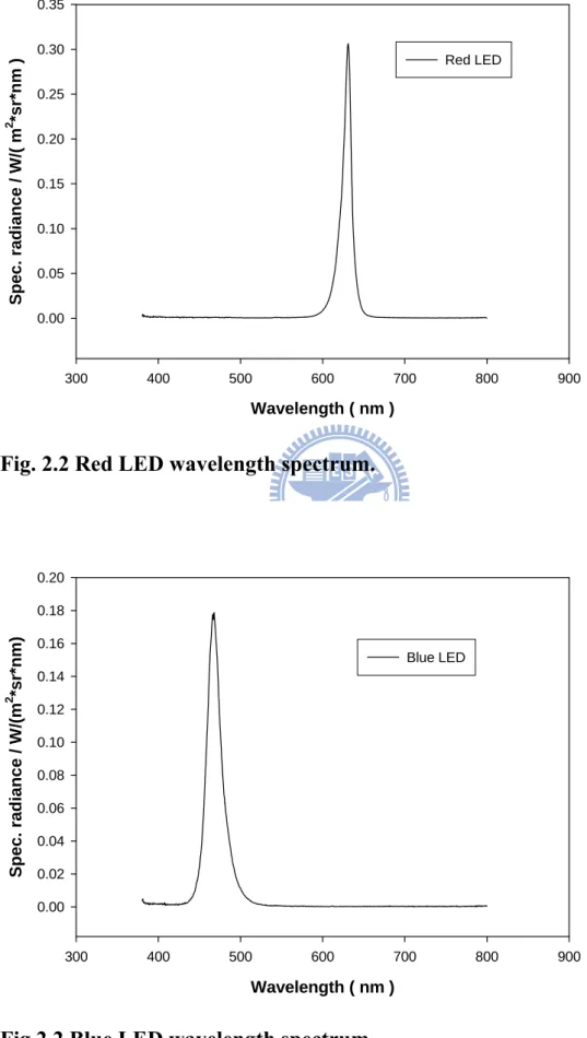
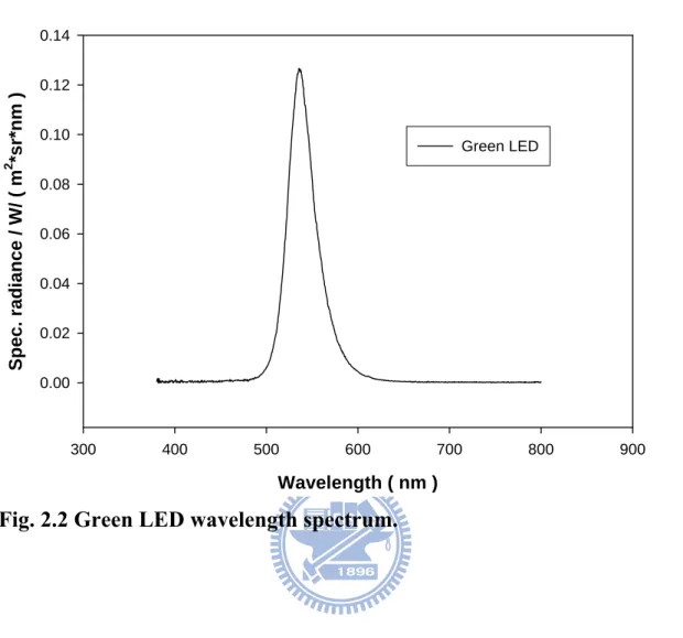
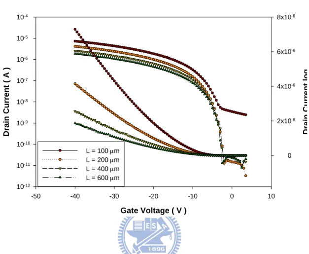
There are four different light sources to illuminate the device in this experiment. The white light source comes from light-emitting diode (LED) backlight with a broad wavelength range. Blue, green and red light sources are light-emitting diodes with 467 nm, 536 and 631 nm wavelengths. These spectrums of four light sources are shown in Fig. 2.2. The light source was set up above the device to irradiate the sample from the top. The light power was controlled by the power supply (PPT3615). The light intensity was adjusted by changing the applied voltage. The light intensity range was
13
from 600 μW/cm2 to 8.5 mW/cm2. Blue, green and red LED was adjust to 50uW/cm2.
2.3 Device Electrical Parameters Extraction
Field effect mobility, threshold voltage, subthreshold slope and Ion/Ioff ratio are usual used to compare different devices’ performance. In the following section, extraction methods would present how to extract parameters from electrical transfer characteristic of pentacene.
2.3.1 Field Effect Mobility
The field effect mobility (μFE) was determined by the orientation of pentacene
molecules near gate dielectric. Therefore, gate dielectric surface states strongly affect the device μFE. The device μFE variation can be used to compare the difference
between PMMA and PVP dielectric layers. In our experiment, μFE were extracted by
using the linear region equation. Because the electrical transfer characteristic of pentacene-based thin film transistor is similar to those conventional single crystalline MOSFETs, the linear region equation can be applied to pentacene-based thin film transistor and can be expressed as
2 1 ( ) 2 DS eff FE GS th DS DS W I C V V V V L μ ⎡ ⎤ = ⎢ − − ⎥ ⎣ ⎦
where Ceff and Vth are effective capacitance per unit area and the threshold voltage. W and L are device channel width and channel length. When operating device at low
14
drain bias, the linear region equation can be modified to
( ) DS eff FE GS th DS W I C V V V L μ = −
After differentiating Eq.(*) with respect to (VG - Vth), the device transconductance can be written as M eff EF DS W G C V L μ =
The field effect mobility can be extracted from the transconductance and this equation
can be expressed as FE M DS eff L G WV C μ =
In this study, we used max GM value to calculate and define the field effect mobility.
2.3.2 Threshold voltage
Threshold voltage (Vth) determines the device operation voltage and smaller Vth
can help to lower power consumption. Because Vth strongly dependents on dielectric
surface states, environmental and fabrication process variations easily cause a shift on the Vth. Based on this phenomenon, the device Vth shift is usually used as an
importance parameter when pentacene-based TFTs applied to Photo detector or Chem-Bio detector. In this study, we used the linear region equation to extract the device Vth.
15
Chapter 3
Result and Discussion
3.1 Characteristics of pentacene-based TFTs with PMMA/SiO
2dielectrics
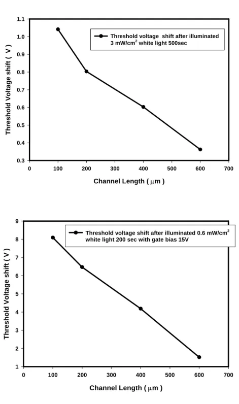
Electrical transfer characteristics of pentacene-based thin film transistor (OTFT) with PMMA dielectric are shown in the Fig 3.1. The device channel length varied from 100 μm to 600 μm while channel width was fixed as 1000 μm. Field effect mobility and threshold voltage are near 0.36 cm2/Vs and -14.5 V extracted from transfer characteristics of devices with different channel widths. The effective capacitance of dual gate dielectric included PMMA and SiO2 dielectrics is near 23.4 nF/cm2. Ion/Ioff ratio of devices with channel length varied from 200 μm to 600 μm are near 106 but Ion/Ioff ratio of device with 100 μm channel length was reduced to 103 due to the large leakage current. In other studies, it was also found that increasing leakage current caused by the short channel effect is a serious problem when improving the device process to short channel.
16
3.2 Electrical Field Dependency of Photo Responsivity
When pentacene-based thin-film transistors (TFTs) are used as switching elements or circuit components, however, light-induced ΔVth causes serious reliability problems. If pentacene-based TFTs are applied to photodetector, the pronounced threshold voltage shift (ΔVth) under light illumination becomes a good reference. The light-induced ΔVth can be attributed to electron trapping in the interface between gate dielectric and active layer. As a result, increasing the interface state density leads to a more significant light-induced ΔVth. Gate-bias stress and drain-bias was also found to enhance the ΔVth under illumination because that the positive gate-bias stress produces extra negative-charged defects.
3.2.1 Drain Bias Modulation on Photo Responsivity
In our previous study, the suppression of light-induced ΔVth has been performed. A fully-suppressed ΔVth by using positive drain-bias stress during illumination was successfully demonstrated. When a positive drain bias is applied, the lowered Fermi energy (EF) in the drain electrode leads to a downward band bending of pentacene
17
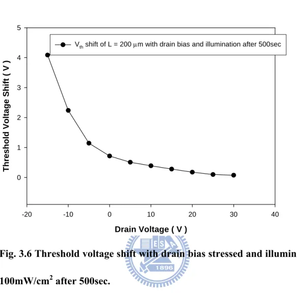
recombine with light-induced electrons. As a result, the electron trapping is suppressed and the ΔVth is reduced. Under illumination, the electron trapping effect competes with the electron-hole recombination effect. It is plausible that when light-induced holes are removed from pentacene through the drain contact, less recombination probability gives rise to more electron trapping and hence larger ΔVth. The negative drain bias creates upward band bending in pentacene and helps light-induced holes to flow out from pentacene into the drain electrode. Enlarged light-induced ΔVth is verified. These expected phenomena are successfully observed in Fig. 3.6 when the light-induced ΔVth is plotted as a function of applied bias (Vapp). In Fig. 3.6, applying drain bias to the device with 200 μm channel length was illuminated for 500-sec.
3.2.2 Gate Bias Modulation on Photo Responsivity
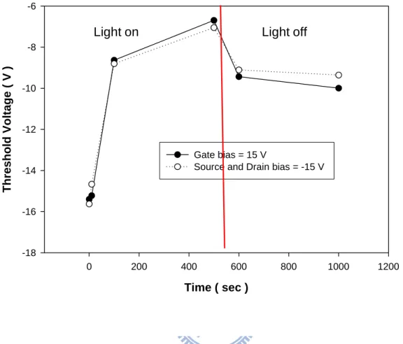
In other hand, it was found that applying the positive gate bias to the device during illumination also can enhance the light-induced ΔVth and the device photoresponsivity. Compare with applying the negative drain bias, applying the positive gate bias can obtain larger light-induced ΔVth as shown in Fig. 3.7. This phenomenon can be explained by using the electrical field distribution in the channel. When illuminating the device, excitons are generated in the channel at beginning.
18
These light-induced excitons need the electrical field to dissociate light-induced excitons into hole-electron pairs. In Fig. 3.8, gate bias induces two strong electrical fields near contact electrodes but drain bias only induces the strong electrical field near drain electrode. In following experiment,
Based on section 3.2.1, applying positive gate bias can take as applying negative source and drain bias simultaneously and further confine the light-induced electrons and enhance ΔVth.
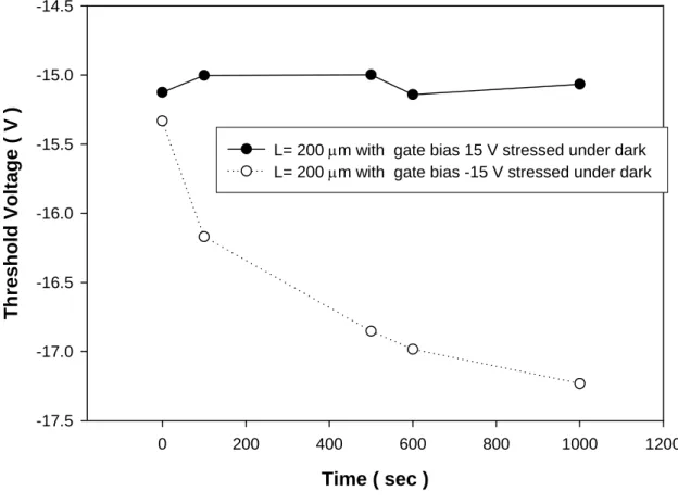
3.2.3 Gate Bias Stress under Dark
Although using drain bias stress and gate bias stress can modulate the device responsivity, the bias stress effect on light-induced ΔVth should be considered. In this experiment, 1000-sec positive and negative gate bias were applied to pentacene-based TFT with PMMA dielectric. After 1000-sec bias stress, ΔVth curves are plotted as a function of the stress time. Obviously, the positive gate bias stress caused slight the device ΔVth. Compare with previous light-induced ΔVth under bias stress, the bias-induced ΔVth can be neglected. For the negative bias stress, the pronounced ΔVth was observed. When combining illumination and negative bias stress, the suppressed ΔVth is due to the compensation between the bias-induced positive charged states and the light-induced negative charged states.
19
3.2.4 Energy-Band Diagrams under Bias Stress
Using energy-band diagrams explains the relationship between gate bias and illumination mechanism. It is known that photons excite electron-hole pairs while illuminating the semiconductor layer. Light-induced electrons fill the trap states on the PMMA dielectric surface to cause a shift forward positive. Gate bias adjusts the Fermi-level of gate metal. Electric field decides the Fermi-level in the band-bending region. The band-bending region will decide the amount of trap states and the maximum ΔVth. And the gate electric field forced the electron-hole pairs to separate.
Energy band diagram is depicted to explain the proposed mechanism. Fig. 3.20 (a) shows energy band diagram under VG= 0V and dark. Fig. 3.20 (b) shows energy band diagram under VG= 0V and illumination. When a positive drain bias is applied, the lowered Fermi energy (EF) in the gate electrode leads to a downward band
bending of pentacene near the gate side as shown in Fig. 3.20 (c). The band bending confines light-induced electrons in the channel to generate electron traps. As a result, the electron trapping is enhanced and theΔVth is enlarged. As shown in Fig. 3.20 (d),
the negative gate bias creates upward band bending in pentacene and helps light-induced holes to confirm in channel to recombine with light-induced electrons. As a result, the electron trapping is suppressed and theΔVth is reduced.
20
electrode leads to a downward band bending of pentacene near the gate dielectric. The downward band bending provides more trap sites which originally exited in the forbidden gap to cause larger light-induced ΔVth. These additional trap sites are limited by gate bias. Therefore, when total trap sites are filled, the light-induced ΔVth reaches the saturation even extending illumination time.
3.3 Channel Length Modulation on Device Responsivity
In previous researches about organic phototransistors, there are few studies to discuss the relationship between the channel length and the device photoresponsivity. In our previous studies, when illuminating the device, extra hole and electron carriers were generated in the channel. Light-induced holes flow out through drain and source electrodes and residual electron carriers cause electron traps in the channel. Trapped electrons cause the device ΔVth forward positive. In Fig. 3.3 (a), a 500-sec white light was illuminated onto devices with channel lengths varied from 100 μm to 600 μm while all electrodes were grounded. The white light intensity was kept at 3000 μW/cm2. In experiment, it was found that extending the device channel length reduced the light-induced ΔVth as shown in Fig. 3.3 (a). When light-induced holes in the channel move forward drain and source electrodes, more holes are recombined with light-induced electrons in longer channel length. Therefore, decreasing the
21
channel length of phototransistor can enhance the device photoresponsivity. In our previous studies, it was also found that combining light and bias stress can enhance the light-induced ΔVth. Because original light intensity combining with bias stress cause saturate light-induced ΔVth, using the original light intensity and the exposure time can not observe the channel length dependency of the device ΔVth. Therefore, light intensity and exposure time in Fig. 3.3 (a) and (b) differ. In Fig. 3.3 (b), a 200-sec white light was illuminated onto devices with channel lengths varied from 100 μm to 600 μm when applying bias to gate electrode and drain/source electrodes were grounded. The white light intensity was kept at 600 μW/cm2. Obviously, the electrical field did not affect the length dependency of light-induced ΔVth but increased light-induced ΔVth. The electrical field promotes dissociating light-induced excitons into hole-electron pairs. Electrical fields close to drain and source electrodes are strongest as shown in Fig. 3.4. However, increasing the channel length does not extend strongest electrical field regions and provides extra channel length for hole-electron recombination. In this experiment, two main methods were described and verified to control the device photoresponsivity.
22
3.4 Recovery of Light-Induced Threshold Voltage Shift
In previous studies, it was found that the light-induced threshold shift can be recovered after removing illumination. But we found that the source and drain biases help sustain the light-induced ΔVth after removing irradiation. In this experiment, it
was found that applying gate bias also can sustain the light-induced ΔVth after
removing irradiation compared as shown in the Fig. 3.11.
In further study, different conditions were discussed to sustain the light-induced ΔVth of pentacene-based TFT with PMMA dielectric after removing light. Following
three conditions were used to compare the retention ability after the light-induced ΔVth reaches saturation. (1) keep VG = 15V in dark, (2) keep VG = 0 V under illumination and (3) keep VG = 0 V in dark. With almost identical initial light-induced
ΔVth, before comparing different conditions, the device was applied by 500 sec
illumination of white light with VG = 15V and the intensity was kept at 600 μW/cm2. When (2) and (3) conditions were performed, the recovery of light-induced ΔVth was
observed as shown in Fig. 3.11. However, for the condition (1), the light-induced ΔVth
is sustained for over 2100 seconds. Fig. 3.11 shows that during white light illumination or gate bias stress, the device ΔVth is slight compared with combining
23
3.5 Photo-Sensibility of Pentacene-Based TFTs
3.5.1 Photo-Sensibility for Light Wavelength
According to the study proposed by Yong-Young Noh, Dong-Yu Kim and Kiyoshi Yase [8], the influence of wavelength on the irradiation effect of pentacene-based OTFTs had been discussed. A smaller light-induced ΔVth was found
when the incident light had larger wavelength due to the internal filter effect. When illuminating the pentacene-based TFTs, the device threshold voltage shifted toward positive because that the light-induced electrons close to the gate dielectric were trapped by the interface states. If the wavelength had high absorption in pentacene, it was not able to arrive at the gate dielectric interface effectively.
In this experiment, red, green and blue light-emitting diodes (LEDs) were used as light sources to discuss light wavelength influence on the device ΔVth. Fig. 3.12 shows that the device ΔVth increased with decreasing light wavelength. Based on the internal filter effect, the light-induced ΔVth was dominated by light absorption
24
3.5.2 The Detectable Light Intensity Range
In most phototransistor studies, these authors tried to research and improve the detectable minimum light intensity of their phototransistors. Therefore, there are a few discussions on the detectable light intensity range of their phototransistors. In section 3.2 and 3.3, we verified applying positive gate bias and scaling down channel length to enhance the device photo sensibility. In this section, the detectable light intensity range of pentacene-based TFTs with PMMA dielectric was discussed by varying the light intensity. First, we discuss the relationship between detectable range and gate bias. After 100-sec white light illumination with different gate bias, the device ΔVth is plotted as a function of the light intensity as shown in the Fig. 3.13. It is found that the device ΔVth reaches the saturation when increasing the light intensity. When increasing gate bias from 5V to 15V, the maximum detectable light intensity is extended from 200 μW/cm2 to 400 μW/cm2. Therefore, applying positive gate bias not only promotes the phototransistor sensitivity but also extends the detectable light intensity range. In following experiment, using different light intensity to illuminate devices observed the saturation time while at fixed gate bias. As expected result, the saturation time was reduced when increasing light intensity but it was found that ΔVth reached same saturate values even if under different light intensity illumination. A band diagram from gate to drain is used to explain the phenomenon. When a positive
25
gate bias is applied, the lowered Fermi energy (EF) in the gate electrode leads to a
downward band bending of pentacene near the gate dielectric. The downward band bending provides more trap sites which originally exited in the forbidden gap to cause larger light-induced ΔVth. These additional trap sites are limited by gate bias. Therefore, when total trap sites are filled, the light-induced ΔVth reaches the saturation even extending illumination time.
3.5.3 The Light-Induced Drain Current Increment
On above discussion, the light-induced ΔVth was referred to predict the light intensity. However, the device photocurrent is the other important parameter should be discussed in detail. In the Fig. 3.15, applying one light pulse with 50-sec pulse width to the device induced drain current increment while gate bias was kept at 15V. The white light was set at 400 μW/cm2. After 50-sec bias stress with illumination, drain current increment was about 2×10⁻⁷ A. When illuminating device without bias, the max saturate drain current increment was only about 4×10⁻⁹ A as shown in Fig. 3.18.
26
3.5.4 Photo Responsivity
In this section, red and blue light emitting diodes and white light backlight were used as light sources. The illumination time was 200-sec duration. Device channel lengths are 100 μm and 200 μm. The device photoresponsivity was plotted as a function of gate bias as shown in Fig. 3.19. For devices with 100 μm channel length, the device photoresponsivity under blue light was largest and the device photoresponsivity under red light was smallest. The similar result was also observed in previous section. When combining blue light illumination and gate bias VG = 30 V, the max device photoresponsivity can reach 92 A/W. When increasing device channel length, the device photoresponsivity was reduced as previous mentions in section 3.3. It was found that applying over large light intensity obviously reduced the device photoresponsivity. It means that the device photocurrent can not continuously be increased with increasing light intensity when the photocurrent reaches saturation. Therefore, based on above results, pentacene-based phototransistors are suitable to detect low power light source.
27
3.6 Operation Method of Pentacene-Based Phototransistors
3.6.1 Recovery of Threshold Voltage Shift
In Fig. 3.21, after removing illumination and gate bias, the ΔVth caused by 500-sec illumination with gate bias 15V was plotted as a function of recovery time. The device ΔVth drastically decreased at the first recover measurement. Because the Fermi-level immediately come back to original value when the bias was removed, a lot of electron traps with short lifetime were covered.
3.6.2 Cycle Measurement with Same Light Intensity
In order to understand the practical phototransistor operation, cycle measurement were performed to check the device stability. The device operation can be separate into two parts: (1) write region: applying gate bias 15V when light was turned on with 600 μW/cm2 and 50-sec. (2) Recover region: applying 50-sec gate bias -25V when light was turned off. The Fig. 3.22 shows that the light-induced ΔVth kept constant after several cycle measurements.
28
3.6.3 Cycle Measurement with Different Light intensity
In Fig3.23, the cycle measurement was performed under gradually increasing the light intensity. The operation can be separated into two parts: (1) write region: applying gate bias 15V when light was turned on 50-sec duration. (2) Recover region: applying 50-sec reversed gate bias when light was turned off. According to increasing light intensity varied from 50 μW/cm2 to 600 μW/cm2, reversed gate bias was increased from -5V to -20V to come back to original Vth. The ΔVth difference between different light intensity is very clear.
3.6.4 Operation Mechanism
In above experiments, the device ΔVth was extracted in every cycle measurement. Using the device ΔVth is difficult to applied phototransistor on practical circuit. In following cycle measurement, the photocurrent was compared with the light-induced ΔVth in every cycle measurement. In the Fig. 3.16, the light intensity varied from 50 μW/cm2 to 600 μW/cm2 and reversed gate bias was kept at -20V. The operation voltage cycle is shown in the Fig. 3.16. Because reversed gate bias was kept at -20V, the light-induced ΔVth can not come back to original value in time. However, the difference of light-induced ΔVth still can be distinguished between different light intensity. If using the photocurrent observes light intensity variation, the difference of
29
the photocurrent also provides clear light intensity difference. However, when eliminating current induced by ΔVth, the photocurrent variation in different light intensity is similar. It means that most photocurrent variation is caused by light-induced ΔVth. The photocurrent increment with and without excluding ΔVth effect was plotted as a function of light intensity as shown in the Fig. 3.16.
30
Chapter 4.
CONCULSION
In this thesis, pentacene-based thin film transistor with PMMA gate-dielectric was fabricated and discussed the photoresponsivity characteristic of the device in detail. When illuminating pentacene-based phototransistors with positive gate bias, a pronounced threshold voltage shift was observed when S.S. and mobility were kept at constant. It was found that the channel length and gate bias can modulate the light-induced threshold voltage shift. The pentacene-based phototransistors have different photoresponsivity when vary light wavelengths and light intensity. When solely stressing or illuminating the device, the slight ΔVth can be observed. The pentacene-based phototransistor in air ambient is stable and environmental variations does not interfere its photoresponsivity. After periodically measuring the light-induced threshold voltage shift and the photocurrent, the pentacene-based phototransistor provide sensible photoresponsivity in low power light intensity ranged from 50 μW/cm2 to 600 μW/cm2. In this study, we separated the device photocurrent into two main parts: (1) positive light-induced threshold voltage shift contribute to extra current. (2) light-induced hole-electron pairs generate extra current. When excluding the light-induced threshold voltage shift effect, the photocurrent became small and the difference between different light intensity was reduced. It was found
31
that the device photoresponsivity is determined by the light-induced threshold voltage shift.
32
Reference
[1] B. Crone, A. Dodabalapur, Y.-Y. Lin, R. W. Filas, Z. Bao, A. LaDuca, R. Sarpeshkar, H. E. Katz, and W. Li, Nature _London_ 403, 521 (2000).
[2] H. Sirringhaus, N. Tessler, and R. H. Friend, Science 280, 1741 (1998). [3] Y. L. Wu, Y. N. Li, S. Gardner, and B. S. Ong, J. Am. Chem. Soc. 127,
614 (2005).
[4] A. L. Briseno, M. Roberts, M. M. Ling, H. Moon, E. J. Nemanick, and Z. Bao, J. Am. Chem. Soc. 128, 3880 (2006).
[5] A. J. Seeds and A. A. A. De Salles, IEEE Trans. Microwave Theory Tech.38, 577 (1990).
[6] M. A. Romero, M. A. G. Martinez, and P. R. Herczfeld, IEEE Trans. Microwave Theory Tech. 44, 2279 (1996).
[7] Y.-Y. Noh, D.-Y. Kim, Y. Yoshida, K. Yase, B.-J. Jung, E. Lim, and H.-K. Shim, Appl. Phys. Lett. 86, 043501 (2005).
[8] Y.-Y. Noh, D.-Y. Kim, and K. Yase, J. Appl. Phys. 98, 074505 (2005). [9] Y. Liang, G. F. Dong, Y. Hu, L. D. Wang, and Y. Qiu, Appl. Phys. Lett.
86, 132101 (2005).
[10] M. C. Hamilton, S. Martin, and J. Kanicki, IEEE Trans. Electron Devices 51, 877 (2004).
33
[11] G. Gu, M. G. Kane, J. E. Doty, and A. H. Firester: Appl. Phys. Lett. 87 (2005) 243512.
[12] D. W. Park, C. A. Lee, K. D. Jung, B. J. Kim, B. G. Park, H. Shin, and J. D. Lee: Jpn. J. Appl. Phys. 46 (2007) 2640.
[13] M. J. Powell: Appl. Phys. Lett. 43 (1983) 597.
[14] Th.B. Singh, N. Marjanovic’, P. Stadler, M. Auinger, G.J.
Matt, S. Gu‥ nes, N.S. Sariciftci, R. Schwo‥diauer, S. Bauer, J. Appl. Phys. 97 (2005) 083714.
[15] Th.B. Singh, N. Marjanovic’, G.J. Matt, N.S. Sariciftci,
R. Schwo‥diauer, S. Bauer, Appl. Phys. Lett. 85 (2004) 5409. [16] L.-L. Chua, J. Zaumsell, J.-F. Chang, E.C.-W. Ou, P.K.-H.
Ho, H. Sirringhaus, R.H. Friend, Nature 434 (2005) 194. [17] A. Sallelo, M.L. Chabinyc, M.S. Yang, R.A. Street, Appl.
Phys. Lett. 81 (2002) 4383.
[18] Lisong Zhou, Alfred Wanga, Sheng-Chu Wu, Jie Sun, Sungkyu Park, and Thomas N. Jackson, Appl. Phys. Lett. 88, 083502 (2006);
[19] Sergey Lamansky, Peter Djurovich, Drew Murphy, Feras Abdel-Razzaq, Hae-Eun Lee, Chihaya Adachi, Paul E. Burrows, Stephen R. Forrest, and Mark
34
E. Thompson, J. Am. Chem. Soc., 2001, 123 (18), pp 4304–4312
[20] Hagen Klauk, Marcus Halik, Ute Zschieschang, Günter Schmid, and Wolfgang Radlik, J. Appl. Phys. 92, 5259 (2002)
[21] S. J. Zilker, C. Detcheverry, E. Cantatore, and D. M. de Leeuw, Appl. Phys. Lett. 79, 1124 (2001)
[22] Cheon An Lee, Dong-Wook Park, Keum-Dong Jung, Byung-ju Kim, Yoo Chul Kim, Jong Duk Lee, and Byung-Gook Park, Appl. Phys. Lett. 89, 262120 (2006) [23] M. J. Powell, C. van Berkel, A. R. Franklin, S. C. Deane and W. I. Milne, Phys.
Rev. B 45, 4160 - 4170 (1992)
[24] John E. Northrup and Michael L. Chabinyc, Phys. Rev. B 68, 041202 (2003) [25] Gong Gu, Michael G. Kane, James E. Doty, and Arthur H. Firester, Appl. Phys.
Lett. 87, 243512 (2005)
[26] RA Street, A Salleo, ML Chabinyc, Phys. Rev. B, vol.68, 085316, 2003 [27] JE Northrup, ML Chabinyc, Phy. Rev. B, vol.68, 041202, 2003
Spe c. radi ance / W/ ( m 2 *sr*nm )
Fig
Fig. 1.1 S
300 0.000 0.002 0.004 0.006 0.008 0.010g. 2.1 Whit
Schematic
400te light wa
c of penta
W 500avelength
35Figure
acene
Wavelength 600h spectrum
e
h ( nm ) 700 whitm.
800 e light 90036 Wavelength ( nm ) 300 400 500 600 700 800 900 Spec. radiance / W/( m 2 *s r* nm ) 0.00 0.05 0.10 0.15 0.20 0.25 0.30 0.35 Red LED
Fig. 2.2 Red LED wavelength spectrum.
Wavelength ( nm ) 300 400 500 600 700 800 900 Spec. radi ance / W /(m 2 *sr* nm) 0.00 0.02 0.04 0.06 0.08 0.10 0.12 0.14 0.16 0.18 0.20 Blue LED
37 Wavelength ( nm ) 300 400 500 600 700 800 900 Spe c . ra di a n c e / W/ ( m 2 *sr *nm ) 0.00 0.02 0.04 0.06 0.08 0.10 0.12 0.14 Green LED
Fig. 2.2 Green LED wavelength spectrum.
38 Gate Voltage ( V ) -50 -40 -30 -20 -10 0 10 Dra in C urrent ( A ) 10-12 10-11 10-10 10-9 10-8 10-7 10-6 10-5 10-4 Dra in C urrent log 0 2x10⁻⁶ 4x10⁻⁶ 6x10⁻⁶ 8x10⁻⁶ L = 100 μm L = 200 μm L = 400 μm L = 600 μm
Fig. 3.1 The ID-VG characteristic of length 100um to 600um of
pentacene device with PMMA.
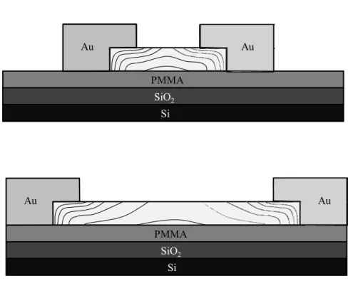
Au Au Au PMMA SiO2 Si Pentacene
39 Channel Length ( μm ) 0 100 200 300 400 500 600 700 Thres hold Voltage shift ( V ) 0.3 0.4 0.5 0.6 0.7 0.8 0.9 1.0 1.1
Threshold voltage shift after illuminated 3 mW/cm2 white light 500sec
Channel Length ( μm ) 0 100 200 300 400 500 600 700 Thr esho ld Vol ta ge shi ft ( V ) 1 2 3 4 5 6 7 8 9
Threshold voltage shift after illuminated 0.6 mW/cm2 white light 200 sec with gate bias 15V
Fig. 3.3 (a) Threshold voltage shift after illuminated with 3mW/cm
2500sec (b) Threshold voltage shift after illuminated with 0.6mW/cm
2and bias stressed 200sec.
40 Au Au Au Au Au PMMA PMMA SiO2 Si Si SiO2
Fig. 3.4 Schematic of the electric field with different length.
Au
Au Au
PMMA Si
SiO2
41 Drain Voltage ( V ) -20 -10 0 10 20 30 40 Th resh old Volta g e Shift ( V ) 0 1 2 3 4 5
Vth shift of L = 200 μm with drain bias and illumination after 500sec
Fig. 3.6 Threshold voltage shift with drain bias stressed and illuminated
100mW/cm
2after 500sec.
42 Time ( sec ) 0 200 400 600 800 1000 1200 Thresho ld Voltage ( V ) -18 -16 -14 -12 -10 -8 -6 Gate bias = 15 V
Source and Drain bias = -15 V
Light on Light off
Fig. 3.7 Light stressed threshold voltage with gate bias and source drain
bias.
43
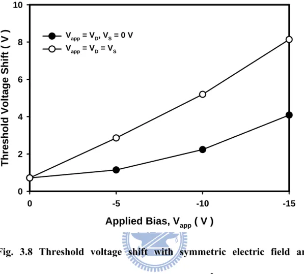
Applied Bias, V
app( V )
-15 -10
-5 0
Threshold Voltage Shift ( V )
0 2 4 6 8 10 Vapp = VD, VS = 0 V Vapp = VD = VS
Fig. 3.8 Threshold voltage shift with symmetric electric field and
asymmetric electric field illuminated 100mW/cm
2after 500sec.
44 Time ( sec ) 0 200 400 600 800 1000 1200 Threshol d Vol tage ( V ) -17.5 -17.0 -16.5 -16.0 -15.5 -15.0 -14.5
L= 200 μm with gate bias 15 V stressed under dark L= 200 μm with gate bias -15 V stressed under dark
Fig. 3.9 Light stressed threshold voltage with positive gate bias and
negative gate bias.
45
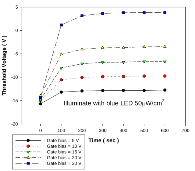
Illuminate with blue LED 50μW/cm
2Time ( sec ) 0 100 200 300 400 500 600 700 Threshold Voltage ( V ) -20 -15 -10 -5 0 5 Gate bias = 5 V Gate bias = 10 V Gate bias = 15 V Gate bias = 20 V Gate bias = 30 V
Fig. 3.10 Blue light stressed threshold voltage with gate bias from
5V~30V.
46
Time ( sec )
0 500 1000 1500 2000 2500 3000
Threshold Voltage Shift ( V )
0 2 4 6 8 10dark with gate bias 15V 2600sec
illuminate ( 17mW/cm2 ) at first 500sec, gate bias15V 2600sec
illuminmate( 17mW/cm2 ) with gate bias 15v at first 500sec with gate bias 15V at first 500sec, illuminate 2600sec illuminate( 17mW/cm2 ) without gate bias 2600sec
Only light 2600sec Only bias 2600sec With light and bias Only bias Only light No light, no bias
47
Wavelength ( nm )
440 460 480 500 520 540 560 580 600 620 640
Threshold Voltage Shift ( V )
0 1 2 3 4 5 6 7 8
Length 100μm device after 200 sec illuminate with gate bias 15V
Fig. 3.12 Length 100um device’s threshold voltage shift after 200second
gate bias stress and illuminate with different wavelength at same
intensity 50uW/cm
2.
48
After 100sec light and gate bias stress
Light Intensity ( μW/cm2 ) 0 100 200 300 400 500 Thr eshold V o ltage S h ift ( V ) 0 1 2 3 4 5 6 Gate bias 5V Gate bias 10V Gate bias 15V
Fig. 3.13 Threshold voltage shift of different light intensity and different
gate bias stress after 200second.
49 Time ( sec ) 0 500 1000 1500 2000 2500 3000 3500
Threshold Voltage ( V
)
-16 -14 -12 -10 -8 -6 -4 50 μW/cm2with gate bias 15V 100 μW/cm2
with gate bias 15V 200 μW/cm2
with gate bias 15V 400 μW/cm2
with gate bias 15V
Channel Length 200 um
Fig. 3.14 Threshold voltage of different light intensity and same gate
bias with period observation.
50 Time ( sec ) 0 100 200 300 400 500 600 ΔDr ain Cu rr ent ( A ) 0.0 5.0e-8 1.0e-7 1.5e-7 2.0e-7 2.5e-7
stressed with illuminate 50μW/cm2
and gate bias 15V stressed with illuminate 200μW/cm2
and gate bias 15V stressed with illuminate 400μW/cm2
and gate bias 15V stressed with illuminate 600μW/cm2
and gate bias 15V
Fig. 3.15 Change of drain current after 50second illuminated and bias
stress.
51
ΔI
ph(
μA )
2.6 2.8 3.0 3.2 3.4Time ( sec )
0 200 400 600 800 1000 1200 1400 1600 1800 2000 2200 0ΔV
th( V )
0 3 6 15 -20 Von V of f 50 μW/cm2 200 μW/cm2 400 μW/cm2 600 μW/cm2Fig. 3.16 Cycle measurement at same stress bias and recover bias with
different light intensity.
52
Fig. 3.17 Error bar of photo current at different light intensity with bias
or without bias
Light Power (
μW/cm
2)
0 100 200 300 400 500 600 700
Photo current increm
ent (
μA )
0.0 0.1 0.2 0.3 0.4 With ΔVth Effect Without ΔVth Effect53
Light itensity ( uW/cm2 )
0 100 200 300 400 500 ΔDra in Cu rre n t ( A ) 0 1e-9 2e-9 3e-9 4e-9 5e-9
measurement First time measurement Second time
54 Gate bias ( V ) 0 5 10 15 20 25 30 35 Pho to reponsiv ity ( A/W ) 0 20 40 60 80 100 L = 200 μm illuminate 600 μW/cm2
L = 100 μm illuminate red LED 50 μW/cm2 L = 100 μm illuminate white light 50 μw/cm2 L = 200 μm illuminate white light 50 μW/cm2 L = 100 μm illuminate Blue LED 50 μW/cm2
With gate bias and illuminate 200sec
Fig. 3.19 Photoresponsivity at different length, wavelength and gate bias
condition
55 Zlab for Thin‐Film Transistors Gate VG=0 qΦM Pentacene qΧ Eg (2.2eV) traps EF SiO2 PMMA qΦAU ELUMO (3.0eV) EHOMO (5.2eV) EFi S/D
Fig. 3.20 Schematic energy-band diagrams for different conditions
(a)V
G= 0 in dark ambient
s
(b) V
G=0 under illuminate
Zlab for Thin‐Film Transistors
Gate SiO2 PMMA
Pentacene VG > 0 EF ELUMO (3.0eV) EHOMO (5.2eV) EFi S/D
56
(c) V
G> 0 under illuminate
Zlab for Thin‐Film Transistors
Gate SiO2 PMMA
Pentacene VG > 0 ELUMO (3.0eV) EHOMO (5.2eV) S/D
(d) V
G<0 under illuminate
57 Time ( sec ) 0 10000 20000 30000 40000 50000 Threshold Voltag e ( V ) -15 -14 -13 -12 -11 -10 -9 -8 -7
Fig. 3.21 Recovery for 12 hour after illuminate 600 μ W/cm
2and gate
bias stress 15V
58 Time ( sec ) 0 200 400 600 800 1000 1200 1400 Th resh ol d V o lt ag e ( V ) -15 -14 -13 -12 -11 -10 -9 Length = 200 μm with 600 μW/cm2
and gate bias 15V
vg15
Vg0
Vg-25
Illuminate with light power 600uW/cm2
Fig. 3.22 Cycle measurement under same light intensity, stress bias and
recovery bias.
59 Time ( sec ) 0 200 400 600 800 1000 Threshold Vol tage Shift ( V ) -0.5 0.0 0.5 1.0 1.5 2.0 2.5 3.0
Length 200 μm device with gate bias 15V and light intensity ( 50μW/cm2, 200μW/cm2, 400μW/cm2, 600μW/cm2 ) 50uW/cm2 with Vg15 Vg-5 200uW/cm2 with Vg15 400uW/cm2 with Vg15 600uW/cm2 with Vg15 Vg-10 Vg-15 Vg-20
Fig 3.23 Cycle measurement with different light intensity and recovery
bias.
60
gate bias stress 5V
Gate Voltage ( V ) -50 -40 -30 -20 -10 0 10 Drain Curr ent ( A ) 10-12 10-11 10-10 10-9 10-8 10-7 10-6 10-5 dark 50μW/cm2 100μW/cm2 200μW/cm2 300μW/cm2 400μW/cm2
61
gate bias stress 10V
Gate Voltage ( V ) -50 -40 -30 -20 -10 0 10 Drain Curre n t ( A ) 10-12 10-11 10-10 10-9 10-8 10-7 10-6 10-5 dark 50μW/cm2 100μW/cm2 200μW/cm2 300μW/cm2 400μW/cm2
62
gate bias stress 15V
Gate Voltage (V)
-50 -40 -30 -20 -10 0 10
D
rain Current (A)
10-12 10-11 10-10 10-9 10-8 10-7 10-6 10-5 dark 50uW/cm22 100uW/cm22 200uW/cm22 300uW/cm22 400uW/cm22
63