國 立 交 通 大 學
電子工程學系 電子研究所碩士班
碩 士 論 文
一種利用鉿矽酸鹽結晶化形成的新穎氧化鉿非揮發
性奈米晶體記憶體
A novel HfO
xnanocrystal nonvolatile memory formed
by HfSiO
4crystallization
研 究 生:林慶宗
指導教授:張俊彥 博士
一種利用鉿矽酸鹽結晶化形成的新穎氧化鉿非揮發性
奈米晶體記憶體
A novel HfO
xnanocrystal nonvolatile memory formed by
HfSiO
4crystallization
研 究 生:林慶宗 Student:Ching-Tzung Lin
指導教授:張俊彥 博士 Advisor:Dr. Chun-Yen Chang
國 立 交 通 大 學
電子工程學系 電子研究所碩士班
碩 士 論 文
A Thesis
Submitted to Department of Electronics Engineering and Institute of Electronics College of Electrical Engineering and Computer Science
National Chiao Tung University in partial Fulfillment of the Requirements
for the Degree of Master
in
Electronics Engineering June 2004
Hsinchu, Taiwan, Republic of China
一種利用鉿矽酸鹽結晶化形成的新穎氧化鉿非揮發
性奈米晶體記憶體
研究生:林慶宗 指導教授:張俊彥 博士
國立交通大學
電子工程學系 電子研究所碩士班
摘 要
在本論文中,我們將研究一種關於在鉿矽酸鹽薄膜中形成氧化鉿奈米晶體的新穎技 術。本實驗是利用在氬氣/氧氣的環境中,共同濺鍍高純度的鉿靶與矽靶來沉積鉿矽酸 鹽薄膜。之後,薄膜進行高溫 900 °C氧氣環境下熱退火處理,氧化鉿奈米晶體將在鉿矽 酸鹽薄膜中結晶產生。其奈米晶體尺寸為 7.8 nm而密度分佈為 9.2×1011 cm-2。此外,我 們也發現到奈米晶體的產生將造成表面崎嶇不平。當鉿矽酸鹽薄膜發生結晶現象時,薄 膜中將分離出複晶氧化鉿和氧化矽,這是因為在薄膜中發生相分離的關係。從電性分析 中顯示,在 900 °C熱退火處理樣本中可獲得大的記憶窗口以及小的漏電流。這是因為在 氧氣環境中高溫熱退火有助於形成奈米晶體和修補矽酸鹽薄膜中的氧空缺。此外,當增 加所施加負閘極電壓時,有更多的電子注入並被奈米晶體補抓故可獲得更大的記憶窗 口。本實驗中,奈米晶體記憶體是經由閘極注入電子來執行寫入操作。從 900 °C熱退火2.2 nm和補抓電荷密度Qt為 4.78×10 -7 C/cm2。我們也發現當提高熱退火溫度將使距心減 少以及補抓電荷增加。最後,我們利用Frenkel-Poole傳導來討論奈米晶體的傳導機制。 結果顯示,900 °C沉積後熱退火處理樣本的等效阻礙高度Φ 為 0.684 eV。因此,我們FP 相信經由鉿矽酸鹽薄膜發生結晶現象所產生的氧化鉿奈米晶體記憶體將是下個世代非 揮發性記憶體最有可能的候選人之一。
A novel HfO
xnanocrystal nonvolatile memory
formed by HfSiO
4crystallization
Student:Ching-Tzung Lin Advisor:Dr. Chun-Yen Chang
Department of Electronics Engineering and Institute of Electronics
National Chiao Tung University
ABSTRACT
We have investigated a novel technique to form the HfO2 nanocrystals in Hf-silicate film.
The Hf-silicate films are deposited by co-sputtering the hafnium and silicon targets in Ar/O2
ambience. From the material analysis, we have found that the HfO2 nanocrystals with a size of
7.8 nm and a dot density of 9.2×1011 cm-2 are formed by Hf-silicate crystallization when it is annealed in O2 ambience at 900 °C. In addition, the surface roughness is dramatically
increased when the nanocrystals are formed. When the Hf-silicate is crystallized, HfOx and
SiOx (x<2) phases are separated, and the polycrystalline HfO2 are obtained. Therefore, we
believe that the formation of nanocrystals is induced by the phase separation of Hf-silicate. The electrical characteristics of HfO2 nanocrystal memory are also investigated by measuring
900 °C annealing are obtained because annealing in O2 ambience is helpful for forming
nanocrystals and repairing the oxygen vacancies in Hf-silicate. Moreover, we have found that more electrons are injected into the nanocrystals as increasing the negative gate voltages to widen the memory window. Thus, the nanocrystal memory should be programmed by gate injection. The centroid ( X ) of 2.2 nm and the trap charge density (Qt) of 4.78×10⁻⁷ C/cm2 are
calculated by the double-IV measurement with CCS of –1 mA/cm2 for the sample with 900 °C annealing. We also find that X is decreased and Qt is increased as raising the annealing
temperature. Finally, the conduction mechanism of the nanocrystal memory is dominated by the Frenkel-Poole emission, and the effective FP barrier heights of 0.684 eV is extracted for the nanocrystals formed in 900 °C annealing. Therefore, the HfO2 nanocrystal memory
formed by Hf-silicate crystallization should be one of the most promising candidates for nonvolatile memory applications.
誌 謝
在兩年的碩士班生活裡,首先要感謝的是我的指導教授張俊彥校長,
在其繁忙的校務工作之餘仍撥冗給予指導與鼓勵,親切的關心學生狀況,
老師寬闊的胸襟與其儒者的風範、氣度更是我學習的目標。再來要感謝的
是國家奈米實驗室的簡昭欣博士,簡博士不只是在學術上給予我指導與啟
發,在生活中更教導了我許多待人處事的道理,很高興在我的碩士生涯中
能遇見這位亦師亦友的好學長。
此外,我還要特別感謝經緯學長、辭修學長以及文泰學長在生活上、
課業上、實驗上、量測上,到最後碩士論文的撰寫所給予我的照顧以及協
助,如果沒有他們的幫忙,這本碩士論文就不會如此順利的產生。尤其是
經緯學長,熬夜幫我修正論文,辛苦了!也感謝國家奈米實驗室呂正傑學
長與許世祿學長在實驗上給予我的許多幫助,使我的實驗能順利進行。嘉
欣、怡誠、凱立、心卉、信宏、小懿學長、峻豪學長,有你們的陪伴讓我
的碩班生活增色不少。還有小賢學長、盈彰,跟你們一起做實驗真的很快
樂!
最後要感謝我的女友舒婷平時對我生活上的照顧與關心。親愛的爸
爸、媽媽以及妹妹,感謝你們長久以來對我的支持、關愛與包容,由於你
們的付出與鼓勵才讓我在學業上能走的如此平暢順利!
Contents
Abstract (Chinese)
i
Abstract (English)
iii
Acknowledgement
v
Contents
vi
Table Captions
viii
Figure Captions
ix
Chapter 1
Introduction
1.1 Background
1
1.2 Motivation
4
1.3 Organization of the Thesis
5
Chapter 2 Experimental procedures
2.1 Device fabrication
6
2.2 Material analysis and electrical characteristics measurement
6
2.2.1 Material analysis
6
2.2.2 Electrical characteristics measurement
7
Chapter 3 Material analysis of nanocrystal in HfSiO
43.1 Nanocrystal formation
8
3.2 Surface roughness analysis
9
3.3 Nanocrystal composition and structure analysis
10
3.3.1 EDS analysis
10
3.3.2 Diffraction pattern
11
3.3.3 XPS analysis
12
3.3.4 Phase separation
13
Chapter 4 Electrical characteristics of nanocrystal in HfSiO
44.1 C-V and I-V characteristics
15
4.2 Gate injection programming
16
4.3 Constant current stress (CCS) and centroid analysis
17
Chapter 5 Conclusion
5.1 Conclusion
20
References
23
Table Captions
Table 4.1 Values of centroid and trapped charge density extracted by double-IV measurement.
Figure Captions
Chapter 1
Fig. 1.1 (a) The schematic of a ETOX flash memory device.
(b) The band diagram of programming and erasing operations. The left shows electron flow during programming by Channel-Hot-Electron (CHE) injection. The right shows electron flow during erasing by Fowler-Nordheim (FN) tunneling to the source [3].
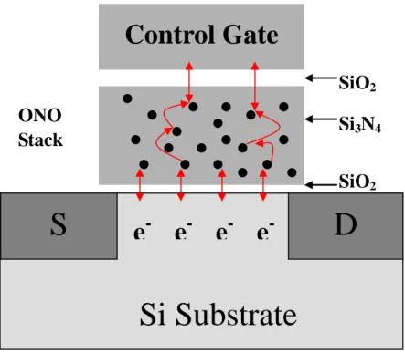
Fig. 1.2 Basic SONOS memory device structure. Arrows show paths of electron transport during memory operation. The electrons hop between trap sites within the Si3N4
layer.
Fig 1.3 (a) An illustration of a nanocrystal memory.
(b) A scanning electron micrograph (SEM) of dense Si-nanocrystal coverage required for reliable nanocrystal memory operation (From Motorola Inc.).
Chapter 2
Fig. 2.1 The process flow of our experiment.
Chapter 3
Fig. 3.1 (a) Cross-section TEM image of as-deposited Hf-silicate film.
Fig. 3.1 (b) Cross-section TEM image of Hf-silicate film with 600 °C O2 PDA.
Fig. 3.1 (c) Cross-section TEM image of Hf-silicate film with 750 °C O2 PDA.
The inset is to enlarge local nanocrystal.
Fig. 3.1 (d) Cross-section TEM image of Hf-silicate film with 900 °C O2 PDA.
The inset is to enlarge a single nanocrystal.
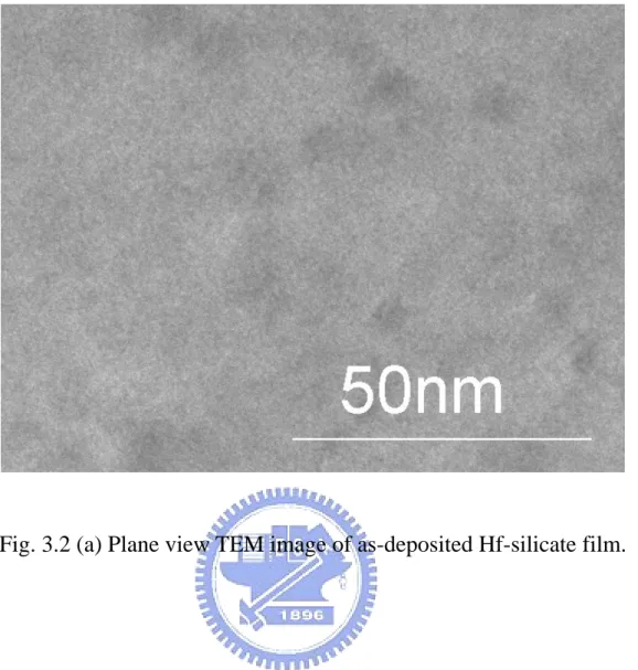
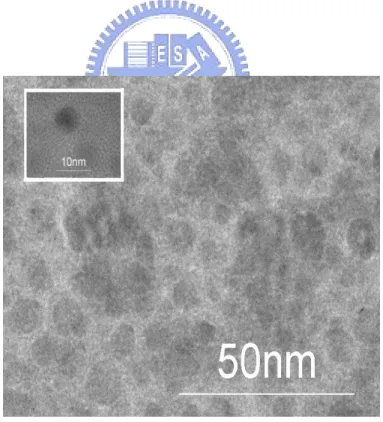
Fig. 3.2 (a) Plane view TEM image of as-deposited Hf-silicate film. Fig. 3.2 (b) Plane view TEM image of Hf-silicate with 750 °C O2 PDA.
Dot density is 4.8×1011 cm-2. The inset is to magnify a single nanocrystal
.
Fig. 3.2 (c) Plane view TEM image of Hf-silicate with 900 °C O2 PDA.
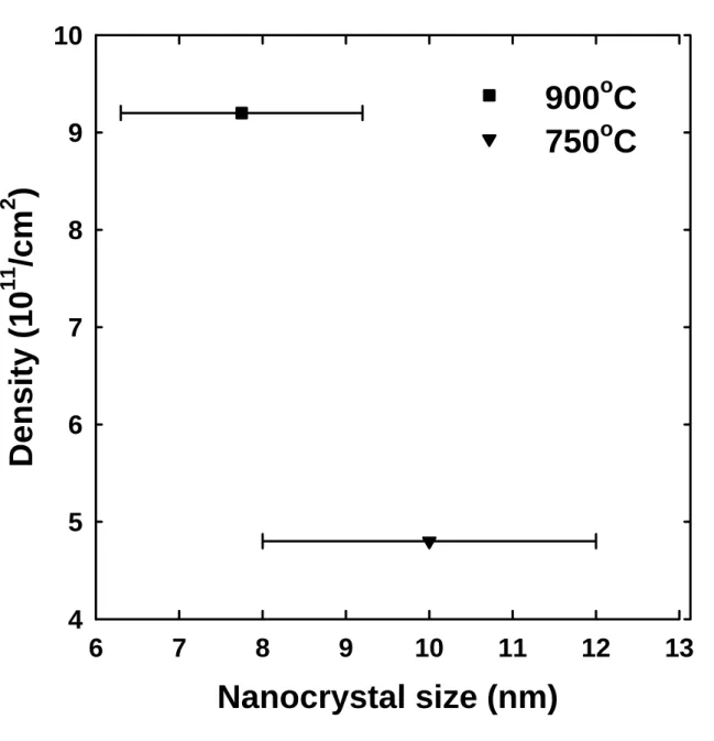
Dot density is 9.2×1011 cm-2. The inset is to magnify a single nanocrystal. Fig. 3.3 Density and size distribution of nanocrystals.
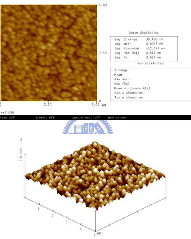
Fig. 3.4 (a) AFM images of as-deposited Hf-silicate film. RMS (Root Mean Square) = 4.614 nm.
Fig. 3.4 (b) AFM images of Hf-silicate film with 600 °C O2 PDA treatment.
RMS = 1.043 nm. The film becomes more dense.
Fig. 3.4 (c) AFM images of Hf-silicate film with 750 °C O2 PDA treatment.
Fig. 3.4 (d) AFM images of Hf-silicate film with 900 °C O2 PDA treatment.
RMS = 18.709 nm.
Fig. 3.5 The surface roughness versus various annealing temperatures of Hf-silicate films. Fig. 3.6 EDS of as-deposited Hf-silicate film.
Fig. 3.7 (a) EDS of inside nanocrystal region with 750 °C O2 PDA treatment.
(b) EDS of outside nanocrystal region with 750 °C O2 PDA treatment.
Fig. 3.8 (a) EDS of inside nanocrystal region with 900 °C O2 PDA treatment.
(b) EDS of outside nanocrystal region with 900 °C O2 PDA treatment.
Fig. 3.9 (a) Diffraction pattern of as-deposited Hf-silicate film.
(b) Diffraction pattern of Hf-silicate film with 750 °C O2 annealing.
(c) Diffraction pattern of Hf-silicate film with 900 °C O2 annealing.
Fig. 3.10 XPS spectra of Hf-silicate film with and without 900 °C O2 PDA.
(a) Spectrum of Hf 4f binding energy. (b) Spectrum of Si 2p binding energy.
Fig. 3.11 (a) Structure of crystalline HfSiO4 showing the Hf bonding to SiO2 units. Hf-O
bonding also exists in and out of the plane of the page [28].
(b) A schematic of Hf-silicate phase diagram. Metastable eutectic between HfO2 and
SiO2 when the HfSiO4 phase is excluded (assuming a phase diagram with no liquid
Chapter 4
Fig. 4.1 (a) C-V characteristics and (b) J-V characteristics of the Hf-silicate film with and without 600 °C O2 PDA.
Fig. 4.2 (a) C-V characteristics and (b) J-V characteristics of the Hf-silicate film after 750 ° C and 900 °C O2 PDA.
Fig. 4.3 (a) C-V characteristics and (b) J-V characteristics of similar EOT that annealing with 900 °C in N2 and O2 ambience
.
Fig. 4.4 Normalized capacitance versus gate voltage plots with different sweeping periods of Hf-silicate with 750 °C O2 PDA.
(a) Negative sweeping periods. (b) Positive sweeping periods.
Fig. 4.5 Normalized capacitance versus gate voltage plots with different sweeping periods of Hf-silicate with 900 °C O2 PDA.
(a) Negative sweeping periods. (b) Positive sweeping periods.
Fig. 4.6 Summaries of memory window versus different sweeping periods shown in Fig. 4.4 and Fig. 4.5.
(a) Apply negative sweeping periods. (b) Apply positive sweeping periods. Fig. 4.7 (a) C-V curves with 5 seconds constant voltage stress (CVS) at +6V.
(b) C-V curves with 5 seconds constant voltage stress (CVS) at –6V. The sample is Hf-silicate film with 750 °C O2 PDA.
Fig. 4.8 (a) C-V curves with 5 seconds constant voltage stress (CVS) at +6V (b) C-V curves with 5 seconds constant voltage stress (CVS) at –6V. The sample is Hf-silicate film with 900 °C O2 PDA.
Fig. 4.9 Respective VG versus time plot under –1 mA/cm2 constant current stress.
(a) The sample is Hf-silicate film with 750 °C O2 PDA.
(b) The sample is Hf-silicate film with 900 °C O2 PDA.
Fig. 4.10 Pre- and post-stress positive and negative I-V plot. The stress condition is –1 mA/cm2 for 100s. The sample is Hf-silicate film with 750 °C O2 PDA.
Fig. 4.11 Pre- and post-stress positive and negative IV plot. The stress condition is -1 mA/cm2 for 100s. The sample is Hf-silicate film after 750 °C O2 PDA.
Fig. 4.12 Schematic of centroid X which is measured from the aluminum gate electrode/nanocrystal film interface.
Fig. 4.13 Leakage current density vs. gate voltage measured at various temperatures. (a) The Hf-silicate film with 750 °C O2 PDA.
(b) The Hf-silicate film with 900 °C O2 PDA.
Fig. 4.14 Temperature dependence of FP leakage current.
(a) Hf-silicate film with 750 °C O2 PDA. The trap height eΦFP is 0.98 eV.
Chapter 1
Introduction
1.1 Background
In 1967, D. Kahng and S. M. Sze invented the first floating-gate (FG) nonvolatile semiconductor memory at Bell Labs [1]. Recently, in order to improve the charge leakage and high power dissipation issues of volatile memory, the nonvolatile semiconductor memory devices play an important role in memory applications because of its low-voltage and low-power features for portable commercial devices. So far, the most widespread nonvolatile memory array is the so-called Flash memory, which has a byte-selectable programming operation combined with a sector erasing at the same time. In addition, as comparing to the electrically programmable read-only memory (EPROM), and electrically erasable and programmable read-only memory (EEPROM), Flash memories have good flexibility of program/erase (P/E) operation, smaller area, and low cost. The most well-known commercial Flash memory is Intel ETOX (EPROM Tunnel Oxide) [2], as illustrated in Fig. 1.1(a). Figure 1.1(b) shows the band diagram of programming and erasing operations. The ETOX is “written” when electrons are injected form channel into the floating gate by Channel-Hot-Electron (CHE) programming and the electrons are “erased” by Fowler-Nordheim (FN) tunneling from FG to source. However, Flash memory has several
main drawbacks. Firstly, the Flash memory needs thick tunnel oxide (8~11 nm) to provide superior retention and endurance characteristics, but it also causes higher operation voltage, slow P/E speed, and poor scalability issues. Secondly, because the polysilicon floating-gate is conductive, the total charges stored in the floating gate will be easily leaked directly through the tunnel oxide when the tunnel oxide is damaged during P/E cycles. To eliminate the issues mentioned above, therefore, the memory-cell structures with discrete traps as the charge storage elements, e.g. MNOS [4], SONOS [5][6], and nanocrystal memory [7][8], have been demonstrated as the promising candidates to replace the Flash memory.
Because semiconductor technology continuously shrinks down to nano scale, the quality of ultra-thin tunnel oxide (<3nm) has been greatly improved. Therefore, nitride-related volume-distributed charge traps memories, such as metal nitride oxide silicon (MNOS) [4] and polysilicon oxide-nitride-oxide silicon (SONOS) [5][6], become more attractive in nonvolatile memory applications. However, the MNOS devices have been shown an issue of charge leakage through the control gate. Then the top blocking oxide has to be introduced into the inter-layer between the control gate and the nitride layer, and it forms the ONO (SiO2-Si3N4-SiO2) gate dielectric stack. Therefore, the SONOS memory devices show greater
retention and program/erase efficiency than MNOS counterparts. Figure 1.2 illustrates the schematic of SONOS structure and the electron conduction paths. When the control gate is biased positively, electrons will tunnel from the channel through the SiO2 into the nitride layer.
However, some electrons in nitride layer continue to move toward the gate but they are blocked by the top oxide. On the other hand, when the control gate is biased negatively, the trapped electrons are ejected into the channel by tunneling process.
Unlike volume-distributed charge traps memories, nanocrystals can be uniformly deposited as a two-dimensional (2-D) distribution on a thin tunnel oxide as illustrated in Fig. 1.3(a). Generally, nanocrystals are small clusters of silicon atoms with size of 5 to 10 nm in diameter as shown in Fig. 1.3(b). By limiting nanocrystal deposition to just one layer and adjusting the thickness of top blocking oxide, charge leakages to the control gate from the storage nodes can be effectively prevented. In recent years, Si and Ge nanocrystals have been studied extensively. IBM researchers, Tiwari et al., first proposed a Si nanocrystal nonvolatile memory with a granular floating gate in 1995 [7], and a higher P/E speed than Flash memory has been reported. In 1998, King et al. has published the Ge dot nanocrystal memory [8]. So far, Si and Ge nanocrystals can be fabricated by various techniques, including chemical vapor deposition [7][9], low energy ion implantation [10], annealing of silicon rich oxide [11], thermal oxidation of SiGe [12], and aerosol nanocrystal formation [13]. Moreover, Lee et al. has reported a new method to improve the memory characteristics of the Si nanocrystal memory devices by replacing the traditional SiO2 with HfO2 high-k dielectrics [14]. In 2002,
Liu et al. has proposed the self-assembled nanocrystal formation process and the design
nanocrystals are formed self-assembly by depositing an ultra-thin metal layer on the gate oxide and then annealing by rapid thermal annealing (RTA) system. In addition, the higher density of states, stronger coupling with the channel, better size scalability, and the design freedom of engineering the work functions to optimize device characteristics are the advantages of metal nanocrystals over their semiconductor counterparts.
1.2 Motivation
To reduce the gate leakage current of MOSFETs with ultra-thin gate oxide, high-k dielectric materials, e.g. ZrO2 [17], HfO2 [18], and their silicates [19], are necessary for
advanced gate insulator applications. Because Hf-silicate has a thin interfacial layer, smooth interface, and good thermal stability [19], Hf-silicate film is demonstrated as one of the promising candidates for an alternate gate dielectric material. However, crystallization behavior of Hf-silicate was observed during a high temperature annealing process, and it severely degrades the performance of devices [20][21]. As been discussed previously [21],
Yamaguchi et al. have shown that the Hf-silicate crystallization is induced by phase
separation. In this thesis, however, we found a new method to form nanocrystals when Hf-silicate crystallization is performed, and they have been shown the potential for nanocrystal memory applications.
1.3 Organization of the Thesis
This thesis can be divided into four parts. In Chapter 1, we briefly introduce the background of nonvolatile memory, including MNOS, SONOS, and Flash memories, and the motivation of forming Hf-silicate nanocrystal memory. We also introduce some fabricating techniques to form nanocrystals. The experimental procedures of depositing Hf-silicate film and nanocrystals formation are described in Chapter 2, and the methods of material analysis and electrical characteristics measurements are also be presented. In Chapter 3, we discuss the results of material analysis, including TEM (Transmission Electron Microscopy), AFM (Atomic Force Microscopy), DP (Diffraction Pattern), EDS (Energy-Dispersive X-ray Spectroscopy), and XPS (X-ray Photoelectron Spectroscopy). From these results, we have demonstrated phase separation induced crystallization and clearly found the nanocrystal formation in Hf-silicate films. In Chapter 4, we show the electrical characteristics of the Hf-silicate film with nanocrystals. The memory window, centroid of electron trapping sites, and conduction mechanism are further investigated. Finally, Chapter 5 presents the conclusions of our experimental results, and we also recommend several suggestions of applying our nanocrystal memory in the next generation.
Chapter 2
Experimental procedures
2.1 Device fabrication
Figure 2.1 shows the process flow of our experiment. The p-type (ρ = 5–10 ohm-cm) 4 inches (100) silicon wafers were prepared as the Si substrate. After being cleaned by RCA process, the 10.5 nm Hf-silicate films were deposited by co-sputtering pure hafnium (99.9% pure) and silicon (99.9% pure) targets under 7.6×10⁻³ torr background pressure with the flow ratio of Ar/O2 = 24 sccm/3 sccm. After depositing the Hf-silicate films, high temperature
post-deposition annealing (PDA) processes were performed at 600 °C, 750 °C, and 900 °C for 60 seconds in O2 ambience. Finally, both the 500 nm aluminum gate electrodes and backside
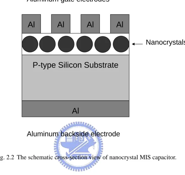
contact were formed by using a thermal evaporation system. The schematic cross-section view of our nanocrystal Metal-Insulator-Semiconductor (MIS) capacitor is shown in Fig. 2.2.
2.2 Material analysis and electrical characteristics measurement
2.2.1 Material analysis
In the study, we used the Field Emission Transmission Electron Microscopy (TEM) to examine the cross-section view, surface morphology, and crystallographic structure of our nanocrystal devices. The physical thickness of Hf-silicate film and the formation of
nanocrystal can be clearly observed by the TEM cross-section images. The size of nanocrystal and the dot density can be calculated by the TEM plane view. The surface roughness and the surface morphology were also examined by Atomic Force Microscopy (AFM) analysis. In addition, the microcrystal structure can be identified by the Diffraction Pattern (DP), and the composition and the element concentration can be defined from the Energy Dispersive X-ray Spectrum (EDS) analysis. The X-ray Photoelectron Spectroscopy (XPS) (1486.6eV Al Kalpha) technique was used to analyze the binding energy and crystallization characteristics of our experimental samples.
2.2.2 Electrical characteristics measurement
The high frequency (100 kHz) capacitance-voltage (C-V) curves were measured by Agilent 4284A LCR meter. From the C-V curves, effective oxide thickness (EOT) can be obtained by accumulation capacitance (EOT = εoxεo/Cacc). Moreover, we defined the memory
windows by the shift of flat-band voltages. The effects of different sweeping bias conditions on memory windows were also investigated. Meanwhile, the current-voltage (I-V) characteristics were measured by Keithley 4200SCS. The leakage current density and the conduction mechanism can be extracted. We also performed constant-voltage stress (CVS) to investigate the polarity dependence of memory windows. After being stressed by constant-current stress (CCS), the centroid of electron trap sites and the trapped charges density (Qt) can be calculated.
Chapter 3
Material analysis of nanocrystal in HfSiO
43.1 Nanocrystal formation
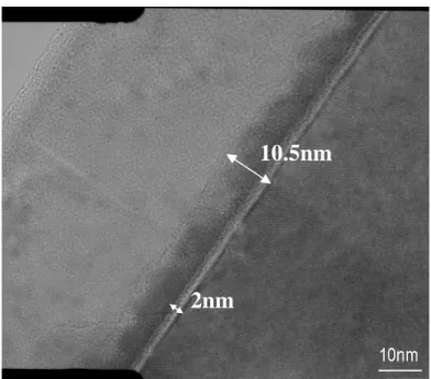
Figure 3.1 illustrates the cross-sectional Transmission Electron Microscopy (TEM) micrograph of Hf-silicate film with different post-deposition annealing (PDA) treatments. From Fig. 3.1(a), we can see the physical thickness of as-deposited film is 10.5 nm and the interfacial layer is about 2 nm. Figure 3.1(b) shows the cross-sectional TEM image of Hf-silicate film after 600 °C O2 post-deposition annealing (PDA), and the physical thickness
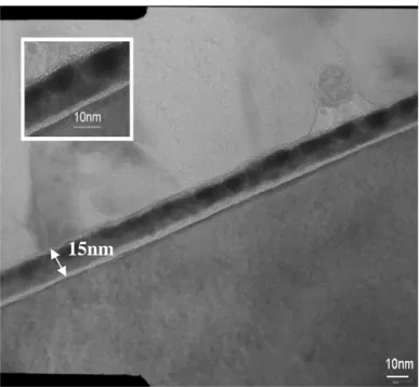
is about 8.5 nm. After being annealed in 600 °C PDA, we can see obviously that the thickness becomes thinner than that of as-deposited film and the interfacial layer is not changed significantly. Besides, no crystallization is observed. Therefore, we believe that 600 °C PDA process helps Hf-silicate film become denser. However, the thicknesses of Hf-silicate films (about 15 nm) are increased when they perform 750 °C and 900 °C O2 PDA process, as shown
in Fig. 3.1(c) and Fig. 3.1(d). We find that Hf-silicate starts to be crystallized after 750 °C O2
annealing. Interestingly, as shown in Fig. 3.1(d), we can clearly see uniform formation of nanocrystals in Hf-silicate film, and the inset displays the size of nanocrystal dot is about 8.5 nm. Figure 3.2 is the TEM plane view of Hf-silicate films. As Fig. 3.2(a) shows, there is no crystallization occurs as the film deposited. From the plane view of the sample with 750 °C
O2 annealing, local crystallization is observed but the nanocrystals are incompletely formed.
Figure 3.2(b) also reveals that the size of nanocrystal is varied from 8 to 12 nm and the average spatially distributing dot density is 4.8×1011 cm-2. However, smaller nanocrystal dots with a size of 6.3 to 9.2 nm are demonstrated by the 900 °C O2 PDA sample. A better uniform
spatial distribution with dot density of 9.2×1011 cm-2 is also obtained in Figure 3.2(c). The dot density versus nanocrystal size is summarized in Fig. 3.3. We speculate that the large variation in nanocrystal size and the nonuniform spatial distribution could be due to not enough heating energy for nanocrystal formation in the condition of 750 °C O2 annealing. Because 900 °C O2
PDA can provide enough energy for nanocrystal agglomeration and formation, we can obtain a higher dot density with smaller average size of 7.8 nm than that of 750 °C O2 PDA
counterpart. Under O2 post-deposition annealing, therefore, we can conclude that the
annealing temperature is the main dominant factor of forming nanocrystals in Hf-silicate films.
3.2 Surface roughness analysis
Surface morphology of our Hf-silicate samples is analyzed by Atomic Force Microscopy
(AFM). Because the Hf-silicate film is deposited by co-sputtering hafnium and silicon targets in O2 ambience, a slight rough surface is induced in the as-deposited films. The Root Mean
3.4(b), however, when the Hf-silicate is performed the 600 °C O2 PDA process, the surface
becomes smoother than that of the as-deposited sample. It is because 600 °C O2 PDA can help
Hf-silicate film become denser and then improve the surface flatness. But, as shown in Fig. 3.4(c), the RMS value of surface roughness is increased to be 8.0 nm. It is corresponding to the crystallization of Hf-silicate with 750 °C O2 PDA. Furthermore, when the nanocrystals are
formed in the condition of 900 °C O2 annealing, the surface roughness is dramatically
increased to 18.7 nm which has been demonstrated in Fig. 3.4(d). Figure 3.5 displays the surface roughness of Hf-silicate films with various annealing temperatures. Although 600 °C annealing can improve the surface morphology, the RMS value will be increased with raising annealing temperature up to 900 °C because of the formation of nanocrystals.
3.3 Nanocrystal composition and structure analysis
3.3.1 EDS analysis
Figure 3.6 shows the EDS spectrum of as-deposited Hf-silicate film. It indicates that the
main composition of the film is Hf, Si, and O with the atomic ratio of 12.6:19:68.4. According to the crystallization behavior discussed above, we applied the EDS technique to analyze the composition inside and outside the crystallization region. The EDS spectrums of Hf silicate films with 750 °C and 900 °C O2 annealing are shown in Fig. 3.7 and Fig. 3.8, respectively.
consisted of Hf and O. It indicates that the nanocrystal is formed by HfOx dot with x<2.
Outside the nanocrystal region, however, the dominant composition is Si and O with the atomic ratio 1:y where y is less than 2. Then, it results in the occurring of phase separation in the Hf-silicate film during high temperature annealing process, and these results are also similar to the previous reports [22][23]. Thus, we believe that the formation of nanocrystals is induced by the phase separation of Hf-silicate. Moreover, because the HfO2 nanocrystals are
isolated by silicon oxide, the leakage through the localized oxide defects of the total store charges is prevented.
3.3.2 Diffraction pattern
The diffraction patterns of samples with different annealing conditions are shown in Fig. 3.9. In Fig. 3.9(a), we observe that the as-deposited Hf-silicate film is amorphous type. On the other hand, after 750 °C annealing the crystallization is occurred by introducing phase separation. Therefore, Fig. 3.9(b) exhibits a typical polycrystalline ring pattern. But the diffraction pattern is complex because of existing many phases in the film, which is due to the incomplete crystallization with insufficient annealing temperature. Comparing with the data sheet of diffraction pattern, we can identify the dominating structure of the local crystal region are monoclinic and tetragonal HfO2. Moreover, we can clearly see a complete diffraction
at 900 °C as displayed in Fig. 3.9(c) [24][25].
3.3.3 XPS analysis
Figure 3.10 demonstrates XPS spectra of Hf-silicate film with and without 900 °C O2 PDA annealing. From Fig. 3.10(a), the spectrum peaks, 4f5/2 (20.5 eV) and 4f7/2 (18.7 eV),
indicates the Hf-O-Si bonds and the binding energy of 12.8 eV is corresponding to the Hf-Si bonds for the as-deposited Hf-silicate film. The Hf-Si bonds are caused by insufficient oxidation when the Hf and Si targets are co-sputtering in O2 ambience. Obviously, after being
annealed at 900 °C, the 4f5/2 (18.9 eV) and 4f7/2 (17.6 eV) Hf-O bonds are observed and the
Hf-Si bonds disappear. In addition, the shifts of 4f5/2 and 4f7/2 peaks are occurred during high
temperature annealing, and the disappearing of Hf-Si bonds means that annealing in O2
ambience helps the re-oxidation of the as-deposited Hf-silicate film. The spectra of Hf-O peaks become slight sharp and that indicates the crystallization of HfO2 [19][26]. The XPS
spectra of Si 2p of Hf-silicate films are illustrated in Fig. 3.10(b). Moreover, the shift of the Si-O bonds (from 102.5 eV to 104 eV) is also observed when the sample is annealed at 900 °C. Again, the shifts of Hf-O and Si-O bonds reveal the phase separation in the Hf-silicate film [26][27].
3.3.4 Phase separation
The atomic structure of Hf-silicate film has been reported as (HfO2)x(SiO2)y shown in
Fig. 3.11(a) [28][29]. According to the results of EDS, DP, and XPS discussed above, the phase separation should be the main mechanism to form the nanocrystals in Hf-silicate films under high temperature annealing. We also have observed that HfO2 and SiO2 will be
separated when the film is crystallized. In the HfO2-SiO2 ternary phase system, the metastable
phase diagrams and phase hierarchies are widely used to explain the phase separation behavior of Hf-silicate film. Fig. 3.11(b) shows the schematic of metastable eutectic between HfO2 and SiO2 when the HfSiO4 phase is excluded, and a eutectic reaction HfSiO4 → SiO2 +
HfO2 can be easily activated when applying sufficient energy. Because the as-deposited
Hf-silicate film is amorphous, it represents a state of high free energy [29]. Therefore, the film can lower its free energy by crystallizing into a metastable phase assembly. The complex structural phases which require extensive atomic rearrangement are kinetically suppressed in favor of structures with simpler atomic arrangement and/or tolerant of disorder. It results in a two-phase assembly consisting of crystalline (monoclinic and tetragonal type) HfO2 and
amorphous SiO2, because the crystallization temperature of SiO2 is higher than that of HfO2
[23]. It should be noted that the formation of a metastable eutectic does not depend on whether the compound is incongruently or congruently melting; the condition is simply that the compound is kinetically excluded in the crystallization process. So we can form the HfO2
nanocrystals in Hf-silicate by elevating the annealing temperature to induce the phase separation behavior.
Chapter 4
Electrical characteristics of nanocrystal in HfSiO
44.1 C-V and I-V characteristics
Figure 4.1 shows the capacitance-voltage (C–V) and current-voltage (I–V) characteristics of the Hf-silicate films with and without 600 °C O2 post-deposition annealing (PDA). In Fig.
4.1(a), we can see that the capacitance of as-deposited film is dropped dramatically under accumulation gate bias because of its higher gate leakage current which is shown in Fig. 4.1(b). The high leakage current is due to a great amount of traps existing in the as-deposited film. However, being annealed by 600 °C PDA process, it can not only improve the C–V curves but also reduce leakage current significantly. It is because the as-deposited film is densified and the traps are repaired during 600 °C O2 annealing. Besides, there are almost no
hysteresis observed for the C–V curves. Additionally, the C–V and I–V characteristics of samples with 750 °C and 900 °C O2 PDA are shown in Fig. 4.2. Obviously, we can see that
the memory window is appeared and it becomes widened from 0.9 V to 1.2 V as increasing the annealing temperature to 900 °C. Because the nanocrystals have been observed in the 750 °C and 900 °C O2 PDA samples by the TEM images, the cause of memory window is
apparently due to the trapping charge characteristics of the nanocrystals [30][31]. Meanwhile, the leakage currents are also reduced as displayed in Fig. 4.2(b). On the other hand, Fig. 4.3(a)
shows that the N2 900 °C PDA process does not results in the memory window as the O2
annealing counterparts does. Thus, we speculate that O2 annealing is helpful for nanocrystal
formation in Hf-silicate films. Although, the O2 annealing sample shows smaller EOT than
that of N2 annealing sample, the leakage current is reduced significantly by the O2 annealing
process as shown in Fig. 4.3(b). Because there are many oxygen vacancies will be produced when nanocrystals are formed, high temperature annealing in O2 ambience is helpful for
repairing the oxygen vacancies and reducing the leakage current.
4.2 Gate injection programming
Figure 4.4 shows the normalized capacitance vs. different sweeping gate voltages of Hf-silicate with 750 °C O2 PDA. When we increase the negative gate bias, a larger memory
window is observed as shown in Fig. 4.4(a). The positive shifts are caused by more electrons are injected into the nanocrystals from gate electrode under higher negative voltages. However, Fig. 4.4(b) shows that there is almost no memory window when the gate biases are applied positively. Therefore, the nanocrystal memory should be programmed by gate injection. These similar results are also illustrated for the 900 °C annealing sample in Fig. 4.5. But Fig. 4.5(a) shows larger memory windows than that of the 750 °C annealing sample. It is due to a higher nanocrystal dot density is obtained after the sample being annealed at 900 °C, and then more electrons can be trapped in the nanocrystal to widen the memory window.
Figure 4.6 summarize the memory window vs. the different applying gate voltages. Obviously, the memory window is increased significantly with negative gate bias in 900 °C annealing sample, and the memory windows are not varied with positive gate biases for both samples. Moreover, Fig. 4.7 shows the C–V curves before and after constant voltage stress (CVS) at ±6 V for 5 seconds of Hf-silicate after being annealed at 750 °C. The hysteresis width is increased insignificantly after being stressed at +6 V gate bias. However, when the sample is stressed at –6 V, a dramatic wide memory window of 1.7 V is obtained. In addition, the stressing process does not affect the memory window because the second stress does not change the window width as shown in Fig. 4.7(b). Again, similar results are observed in Fig. 4.8 for the sample annealed at 900 °C except it shows a magnificent memory window after being stressed at –6 V.
4.3 Constant current stress (CCS) and centroid analysis
Figure 4.9 show the variations of gate voltages, VG, versus time when the samples are
stressed under constant current stress (CCS) of -1 mA/cm2 applied to the gate electrode. The monitoring values of VG become more negative and it indicates that electrons are trapped in
the nanocrystal during constant current stress [32]. Therefore, in order to quantify the amount of trapped charges, the double-IV measurement [33] was performed. This technique involves measuring the voltage shifts on I–V characteristics (both positive and negative bias) of the
nanocrystal MIS structure. Figure 4.10 and Fig. 4.11 show the results of the double-IV measurements after the samples being stressed under a constant current of –1 mA/cm2 for the nanocrystals formed at 750 °C and 900 °C, respectively. The trapped charge density, Qt, and
its centroid, X , can be calculated by the following equations [33][34]. ( o ox G G t ox V V Q t ε ε ∆ ++ ∆ − = ) (4.1) G ox G G V X t V V + + ∆ = ∆ + ∆ − (4.2)
where εox is the dielectric constant of oxide. Comparing the I–V curves of samples before and after stress, ∆VG+ and ∆VG− are the voltage shifts toward positively and negatively, respectively. Then, Qt and X of samples with 750 °C and 900 °C PDA conditions can be
evaluated, and all of the calculated results are summarized in Table 4.1. We find that X is decreased and Qt is increased when we raise the annealing temperature. The increase of Qt is
due to the complete formation of nanocrystals under 900 °C annealing. Finally, according to the data we have obtained, we propose a schematic model of trapping position in nanocrystal MIS structure as illustrated in Fig. 4.12. Because the centroid X is defined as a distance from the top aluminum gate to the effective trapping sites, we can speculate that electrons should be trapped in the nanocrystals.
4.4 Conduction mechanism
measured at various temperatures (25 °C ~ 150 °C). It is clearly observed that in the high voltage (VG > 2 V), the leakage currents are increased with temperatures and show strongly
temperature dependence for both samples. Moreover, because nanocrystals have a great amount of electron traps, we believe the conduction mechanism of leakage current should be dominated by the Frenkel-Poole (FP) emission [35][36]. The following shows the expression of the Frenkel-Poole current:
1/ 2 0exp FP FP B E J J k T β ⎛ − Φ ⎞ = ⎜ ⎝ ⎠⎟ (4.3)
where J0 =σ0 E is the low field current density, σ0 is the low field conductivity, 3
0
( / ) FP e
1/ 2
β = πε ε , and is the effective barrier height of trap sites. After Eq. (4.3) is rearranged, we can obtain a linear relationship between leakage current and temperature as follows: FP Φ 0 1 ln ln( ) FP FP B B E J J T k k β ⎛Φ ⎞ = − ⎜⎜ − ⎝ ⎠⎟⎟ (4.4) Base on the Eq. (4.4), we can plot the ln J vs. 1000/T as shown in Fig. 4.15. Therefore, the values of effective barrier heights of FP emission can be extracted from the slopes. The obtained of samples with 750 °C and 900 °C annealing are around 0.98 eV and 0.684 eV, respectively. We can see that the effective
FP Φ
FP
Φ is lowered when the crystallization temperature is elevated.
Chapter 5
Conclusion
5.1 Conclusion
We have investigated a novel technique to form the HfO2 nanocrystals in Hf-silicate film
for the applications of the nonvolatile memories. The Hf-silicate films are deposited by co-sputtering the hafnium and silicon targets in Ar/O2 ambience. From the material analysis,
we have found that the HfO2 nanocrystals are formed by Hf-silicate crystallization when it is
annealed in O2 ambience at a high temperature (> 750 °C). The nanocrystal size of 7.8 nm and
the dot density of 9.2×1011 cm-2 are observed by the sample with 900 °C O2 PDA from the
TEM images. A uniform spatial distribution is also demonstrated. However, the AFM results show that the surface roughness is dramatically increased when the nanocrystals are formed. As shown by the EDS spectra, the compositions inside and outside the nanocrystals are HfOx
and SiOx (x<2), respectively. When the Hf-silicate is crystallized, the monoclinic and
tetragonal types HfO2 are found by diffraction pattern. The phase separation induced
Hf-silicate crystallization can be explained by the binding energy shifts of Hf-O and Si-O in XPS spectra and the metastable HfO2-SiO2 ternary phase diagram. Therefore, we believe that
the formation of nanocrystals is induced by the phase separation of Hf-silicate.
the Hf-silicate is treated by O2 annealing process at high temperature, the C–V curves with
wide memory windows are obtained, and the leakage currents are also reduced. It is because annealing in O2 ambience is helpful for forming nanocrystals and repairing the oxygen
vacancies. Moreover, by measuring C–V characteristics under different gate sweeping voltages, we have found that more electrons are injected into the nanocrystals as increasing gate voltages more negatively and the memory window is independent of positive biases. Besides, the results of CVS also indicate that the memory window is opened with negative gate voltage and the stress does not induce excess trap sites. Therefore, the nanocrystal memory should be programmed by gate injection. The centroid ( X ) and the trap charge density (Qt) are calculated by the results of I–V characteristics before and after the samples
being stressed under CCS of –1 mA/cm2. We find that X is decreased and Qt is increased
when we raise the annealing temperature. It indicates that the charges are trapped in the nanocrystals near the gate electrode, and the increase of Qt is due to the complete formation of
nanocrystals. Finally, we investigate the conduction mechanism of the nanocrystal memory, and it is dominated by the Frenkel-Poole emission. The effective FP barrier heights are 0.98 eV and 0.684 eV for the nanocrystals are formed in 750 °C and 900 °C annealing, respectively.
In our study, therefore, the HfO2 nanocrystal memory formed by Hf-silicate
that it should be one of the most promising candidates for next generation nonvolatile memory device.
References
[1] D. Kahng and S. M. Sze, Bell Syst. Tech, J., 46, 1288 (1967).
[2] Stephen Keeney, “A 130nm Generation High Density ETOXTM Flash Memory Technology,” IEDM Tech. Dig., p.41-44, 2001.
[3] Aaron Thean, and Jean-Pierre Leburton, “Flash memory : towards single-electronics,”
IEEE Potentials, p.35-41, 2002.
[4] S. M. Sze, “Physics of Semiconductor Devices,” 2nd Edition, John Wiley and Sons, p.504, 1983.
[5] Boaz Eitan, Paolo Pavan, Ilan Bloom, Efraim Aloni, Aviv Formmer, and David Finzi, “NROM:A Novel Localized Trapping, 2-Bit Nonvolatile Memory Cell,” IEEE Electron
Device Letters, Vol.21, No.11, November 2000.
[6] Jiankang Bu, and Marvin H. White, “Effects of Two-step High Temperature Deuterium Anneals on SONOS Nonvolatile Memory Devices,” IEEE Electron Device Letters, Vol.22, No.1, January 2001.
[7] S. Tiwari, F. rana, K. Chan, H. Hanafi, W. Chan, and D. Buchanan, “Volatile and
Non-volatile Memories in Silicon with Nano-Crystal Storage,” IEDM Tech. Dig., p.521-524, 1995.
Nanocrystals Formed by Thermal Oxidation of Si1-xGex ,” IEDM Tech. Dig., p.115-118,
1998.
[9] K. Han, I. Kim, and H. Shin, “Programming characteristics of p-channel Si nano-crystal memory,” IEEE Electron Device Letters, Vol.21, No.6, pp.313-315, June 2000.
[10] H. I. Hanafi, S. Tiwari, and I. Khan, “Fast and long retention-time nano-crystal memory,” IEEE Trans. Electron Devices, Vol.43, pp.1553-1558, September 1996.
[11] Ya-Chin King, Tsu-Jae King, Chenming Hu, “A long-refresh dynamic / quasi-nonvolatile memory device with 2-nm tunneling oxide,” IEEE Electron Device Letters, Vol.20, pp.409-411, August 1999.
[12] Y.-C. King, T.-J. King, and C. Hu, “Charge-trap memory device fabricated by oxidation of Si1-xGex ,” IEEE Trans. Electron Devices, Vol.48, pp.696-700, April 2001.
[13] J. De Blauwe, M. Ostraat, M. L. Green, G. Weber, T. Sorsch, A. Kerber, F. Klemens, R. Cirelli, E. Ferry, J. L. Grazul, F. Baumann, Y. Kim, W. Mansfield, J. Bude, J. T. C. Lee, S. J. Hillenius, R. C. Flagan and H. A. Atwater, “A novel, aerosol-nanocrystal floating gate device for nonvolatile memory applications,” IEDM Tech. Dig., pp.683-686, 2000. [14] J. J. Lee, X. Wang, W. Bai, N. Lu, J. Liu, and D. L. Kwong, “Theoretical and
Experimental Investigation of Si Nanocrystal Memory Device with HfO2 High-k
Tunneling Dielectric,” VLSI Tech. Dig., 2003.
“Metal Nanocrystal Memories—Part I: Device Design and Fabrication,” IEEE
Transactions on Electron Devices, Vol.49, No.9, September 2002.
[16] Zengtao Liu, Chungho Lee, Venkat Narayanan, Gen Pei, and Edwin Chihchuan Kan, “Metal Nanocrystal Memories—Part II: Electrical Characteristics,” IEEE Transactions
on Electron Devices, Vol.49, No.9, September 2002.
[17] Yudong Kim et al., “Conventional n-channel MOSFET devices using single layer HfO2
and ZrO2 as high-k gate dielectrics with polysilicon gate electrode,” IEDM Tech. Dig.,
pp.455-458, 2001.
[18] B. Tavel et al., “High Performance 40nm nMOSFETs With HfO2 Gate Dielectric and
Polysilicon Damascene Gate,” IEDM Tech. Dig., pp.425-432, 2002.
[19] G. D. Wilk, R. M. Wallace, and J. M. Anthony, “Hafnium and zirconium silicates for advanced gate dielectrics,” Journal of Applied Physics, Vol.87, No.1, 1 January 2000 [20] M. R. Visokay, J. J. Chambers, A. L. P. Rotondaro, A. Shanware, and L. Colombo,
“Application of HfSiON as a gate dielectric material,” Appl. Phys. Lett., Vol.80, pp.3183-3185, 2002.
[21] Takeshi Yamaguchi, Ryosuke Iijima, Tsunehiro Ino, Akira Nishiyama, Hideki Satake, and Noburu Fukushima, “Additional Scattering Effects for Mobility Degradation in Hf-silicate Gate MISFETs,” IEDM Tech. Dig., pp.621-624, 2002.
Zhiqiang Chen, and Susanne Stemmer, “Phase Separation in Hafnium Silicates for Alternative Gate Dielectrics,” Journal of The Electrochemical Society, pp.F173-F177, 2003.
[23] Shin-ichi Saito, Yuichi Matsui, Kazuyoshi Torii, Yasuhiro Shimamoto, Masahiko Hiratani, and Shin’ichiro Kimura, “Inversion Electron Mobility Affected by Phase Separation in High-Permittivity Gate Dielectrics,” Jpn. J. Appl. Phys. Vol.42, pp.L1425-L1428, Part 2, 1 December 2003.
[24] D. A. Neumayer, and E. Cartier, “Materials characterization of ZrO2-SiO2 and HfO2-SiO2
binary oxides deposited by chemical solution deposition,” Journal of Applied Physics, Vol.90, No.4, 15 August 2001.
[25] J Zhu, Z G Liu, and Y Feng, “Thermal stability and electrical properties of pulsed laser-deposited Hf-silicate thin films for high-k gate dielectric applications,” J. Phys. D:
Appl. Phys. 36, pp.3051-3056, 2003.
[26] M. A. Quevedo-Lopez, M. El-Bouanani, B. E. Gnade, R. M. Wallace, M. R. Visokay, M. Douglas, M. J. Bevan, and L. Colombo, “Interdiffusion studies for HfSixOy and ZrSixOy
on Si,” Journal of Applied Physics, Vol.92, No.7, 1 October 2002.
[27] Jong-Cheol Lee, S.-J. Oh, Moonju Cho, Cheol Seong Hwang, and Ranju Jung, “Chemical structure of the interface in ultrathin HfO2/Si films,” Appl. Phys. Lett. Vol.84,
[28] G. D. Wilk, R. M. Wallace, and J. M. Anthony, “High-k gate dielectrics: Current status and materials properties considerations,” Journal of Applied Physics, Vol.89, No.10, 15 May 2001.
[29] Susanne Stemmer, Zhiqiang Chen, Carlos G. Levi, Patrick S. Lysaght, Brenden Foran, John A. Gisby, and Jeff R. Taylor, “Application of Metastable Phase Diagrams to Silicate Thin Films for Alternative Gate Dielectrics,” Jpn. J. Appl. Phys. Vol.42, pp.3593-3597, Part 1, June 2003.
[30] Shaoyun Huang et al., “Electron trapping, storing, and emission in nanocrystalline Si dots by capacitance-voltage and conductance-voltage measurements,” Journal of Applied
Physics, Vol.93, No.1, January 2003.
[31] Nae-Man Park, Sang Hyeob Kim, and Gun Yong Sung, “Charging Effect in Amorphous Silicon Quantum Dots Embedded in Silicon Nitride,” Journal of the Korean Physical
Society, Vol.42, pp.S361-S366, February 2003.
[32] D. J. DiMaria, “Determination of insulator bulk trapped charge densities and centroids from photocurrent-voltage characteristics of MOS structures,” Journal of Applied
Physics, Vol.47, No.9, September 1976.
[33] K. S. Lim, and C. H. Ling, “Charge Trapping in Interpoly ONO Film,” ICSE Proc., November 1998.
Transactions on Electron Devices, vol.31, No.9, September 1984.
[35] Po-Tsun Liu, T. C. Chang, Shuo-Ting Yan, Chun-Huai Li, and S. M. Sze, “Electrical Transport Phenomena in Aromatic Hydrocarbon Polymer,” Journal of The
Electrochemical Society, 2003.
[36] W. J. Zhu et al., “Current Transport in Metal/Hafnium Oxide /Silicon Structure,” IEEE
Floating gate
Block Oxide
Tunnel Oxide
S
D
CHE
Program
rase
FN E
Si Substrate
Control Gate
(a)
(b)
Fig. 1.1 (a) The schematic of a ETOX flash memory device. (b) The band
diagram of programming and erasing operations. The left shows
electron flow during programming by Channel-Hot-Electron (CHE)
injection. The right shows electron flow during erasing by
Fowler-Nordheim (FN) tunneling to the source [3].
e
-e
-e
-e
-Si Substrate
S
SiO
2ONO
Stack
D
Control Gate
SiO
2Si
3N
4Fig. 1.2 Basic SONOS memory device structure. Arrows show paths of electron
transport during memory operation. The electrons hop between trap
sites within the Si
3N
4layer.
(a)
(b)
Fig. 1.3 (a) An illustration of a nanocrystal memory. (b) A scanning electron
micrograph (SEM) of dense Si-nanocrystal coverage required for
reliable nanocrystal memory operation (From Motorola Inc.).
Block Oxide
Tunnel Oxide
Control Gate
Nanocrystals
Si Substrate
S
D
RCA clean
P-type Silicon
Co-sputter deposition with Hf and Si targets Hf-silicate
P-type Silicon
Ar / O2 = 24 sccm/ 3 sccm
Pressure = 7.6 x 10⁻³ torr
Fig. 2.1 The process flow of our experiment.
P-type Silicon
Hf-silicate O2 anneal at 600 °C, 750 °C, 900 °C
Hf-silicate P-type Silicon
Aluminum evaporation (shadow mask)
Hf-silicate P-type Silicon
Aluminum gate electrodes
Fig. 2.2 The schematic cross-section view of nanocrystal MIS capacitor.
Al
Al
Al
Al
Nanocrystals
P-type Silicon Substrate
Al
2nm
10.5nm
Fig. 3.1 (a) Cross-section TEM image of as-deposited Hf-silicate film.
8.5nm
15nm
Fig. 3.1 (c) Cross-section TEM image of Hf-silicate film with 750 °C O
2PDA.
The inset is to enlarge local nanocrystal.
15nm
Fig. 3.1 (d) Cross-section TEM image of Hf-silicate film with 900 °C O
2PDA.
The inset is to enlarge a single nanocrystal.
Fig. 3.2 (b) Plane view TEM image of Hf-silicate with 750 °C O
2PDA. Dot
density is 4.8×10
11cm
-2. The inset is to magnify a single nanocrystal.
Fig. 3.2 (c) Plane view TEM image of Hf-silicate with 900 °C O
2PDA. Dot
density is 9.2×10
11cm
-2. The inset is to magnify a single nanocrystal.
Nanocrystal size (nm)
6
7
8
9
10
11
12
13
4
5
6
7
8
9
10
900
oC
750
oC
)
11 2/cm
y (10
Densi
t
Fig. 3.4 (a) AFM images of as-deposited Hf-silicate film. RMS (Root Mean
Square) = 4.614 nm.
Fig. 3.4 (b) AFM images of Hf-silicate film with 600 °C O
2PDA treatment.
RMS = 1.043 nm. The film becomes more dense.
Fig. 3.4 (c) AFM images of Hf-silicate film with 750 °C O
2PDA treatment.
RMS = 8.018 nm.
Fig. 3.4 (d) AFM images of Hf-silicate film with 900 °C O
2PDA treatment.
RMS = 18.709 nm.
Annealing Temperature
asdep
600C
750C
900C
RMS (nm)
0
2
4
6
8
10
12
14
16
18
20
Fig.
3.5 The surface roughness versus various annealing temperatures of
Atomic ratio Hf : Si : O = 12.6 : 19 : 68.4
Inside nanocrystal
HfO
x, X<2
(a)
Outside nanocrystal
SiO
x, X<2
(b)
Fig. 3.7 (a) EDS of inside nanocrystal region with 750 °C O
2PDA treatment.
(b) EDS of outside nanocrystal region with 750 °C O
2PDA treatment.
Inside nanocrystal
HfO
x, X<2
(a)
Outside nanocrystal
SiO
x, X<2
(b)
Fig. 3.8 (a) EDS of inside nanocrystal region with 900 °C O
2PDA treatment.
(b) EDS of outside nanocrystal region with 900 °C O
2PDA treatment.
(a)
(b)
(c)
Fig. 3.9 (a) Diffraction pattern of as-deposited Hf-silicate film. (b) Diffraction
pattern of Hf-silicate film with 750 °C O
2annealing. (c) Diffraction
pattern of Hf-silicate film with 900 °C O
2annealing.
Binding Energy (eV) 10 12 14 16 18 20 22 24 26 Counts (a.u.) 0 5000 10000 15000 20000 25000 30000 35000 asdep 900oC PDA Hf-O-Si Hf-O
Hf 4f
H HffOO22 Hf-Si H Hff--ssiilliiccaattee(a)
Binding Energy (eV)
98 100 102 104 106 108 110 Counts (a.u.) 200 250 300 350 400 450 500 asdep 900oC PDA Si-O Si-O
Si 2p
H Hff--ssiilliiccaattee S SiiOO22(b)
Fig. 3.10 XPS spectra of Hf-silicate film with and without 900 °C O
2PDA.
(a) Spectrum of Hf 4f binding energy. (b) Spectrum of Si 2p
Hf
(a)
H
fS
iO
4SiO
2HfO
2(b)
Fig. 3.11 (a) Structure of crystalline HfSiO
4showing the Hf bonding to SiO
2units. Hf-O bonding also exists in and out of the plane of the page [28].
(b) A schematic of Hf-silicate phase diagram. Metastable eutectic
between HfO
2and SiO
2when the HfSiO
4phase is excluded (assuming
a phase diagram with no liquid immiscibility). Some of the stable
phase fields were excluded for clarity [29].
Gate Voltage, VG (V) -4 -3 -2 -1 0 1 2 3 4 Ca pacitance (pF) -100 0 100 200 300 400
asdep inv to acc asdep acc to inv
600oC inv to acc 600oC acc to inv
(a)
(b)
Gate Voltage, VG (V) -4 -3 -2 -1 0 1 2 3 4 Gat e Cu rren t De nsity , J G (A /cm 2 ) 10-11 10-10 10-9 10-8 10-7 10-6 10-5 10-4 10-3 10-2 10-1 100 101 102 asdep negative asdep positive 600oC negative 600oC positiveFig. 4.1 (a) C-V characteristics and (b) J-V characteristics of the Hf-silicate film
with and without 600 °C O
2PDA.
Gate Voltage, VG (V) -4 -3 -2 -1 0 1 2 3 4 Capacitance (pF) 0 20 40 60 80 100 120 140 160 180 200 750oC inv to acc 750oC acc to inv 900oC inv ot acc 900oC acc to inv
1.2V
0.9V
(a)
(b)
Gate Voltage, VG (V) -4 -3 -2 -1 0 1 2 3 4 Gat e Cu rren t De nsity , J G (A/cm 2 ) 10-11 10-10 10-9 10-8 10-7 10-6 10-5 10-4 750oC neagtive 750oC positive 900oC negative 900oC positiveFig. 4.2 (a) C-V characteristics and (b) J-V characteristics of the Hf-silicate film
after 750 °C and 900 °C O
2PDA.
Gate Voltage, VG (V) -4 -3 -2 -1 0 1 2 3 4 Capa citance (pF) 0 50 100 150 200 250 N2900oC acc to inv N2900oC inv to acc O2900oC acc to inv O2900oC inv to acc EOT~8 nm EOT~8.6 nm
(a)
Gate Voltage, VG (V) -4 -3 -2 -1 0 1 2 3 4Gate Current Density, J
G (A /cm 2 ) 10-12 10-11 10-10 10-9 10-8 10-7 10-6 10-5 10-4 10-3 10-2 N2900oC negative N2900oC positive O2900oC negative O2900oC positive
(b)
Fig. 4.3 (a) C-V characteristics and (b) J-V characteristics of similar EOT that
annealing with 900 °C in N
2and O
2ambience.
Gate Voltage, VG (V) -6 -4 -2 0 C/ Cmax 0 1 -2V -> 1V -3V -> 1V -4V -> 1V -5V -> 1V -6V -> 1V
(a)
Gate Voltage, VG (V) -2 0 2 4 6 C/C ma x 0 1 1V -> -2V 2V -> -2V 3V -> -2V 4V -> -2V 5V -> -2V 6V -> -2V(b)
Fig. 4.4 Normalized capacitance versus gate voltage plots with different
sweeping periods of Hf-silicate with 750 °C O
2PDA. (a) Negative
sweeping periods. (b) Positive sweeping periods.
Gate Voltage, VG (V) -6 -4 -2 0 C/C max 0 1 -2V -> 1V -3V -> 1V -4V -> 1V -5V -> 1V -6V -> 1V
(a)
Gate Voltage, VG (V) -2 0 2 4 6 C/C max 0 1 1V -> -2V 2V -> -2V 3V -> -2V 4V -> -2V 5V -> -2V 6V -> -2V(b)
Fig. 4.5 Normalized capacitance versus gate voltage plots with different
sweeping periods of Hf-silicate with 900 °C O
2PDA. (a) Negative
sweeping periods. (b) Positive sweeping periods.
Apply Vacc (V) -7 -6 -5 -4 -3 -2 M e mo ry Win dow (V) 0 1 2 750oC 900oC
(a)
Apply Vinv (V) 1 2 3 4 5 6 7 M e mory Window (V) 0.04 0.06 0.08 0.10 0.12 0.14 750o C 900oC(b)
Fig. 4.6 Summaries of memory window versus different sweeping periods
shown in Fig. 4.4 and Fig. 4.5. (a) Apply negative sweeping periods.
(b) Apply positive sweeping periods.
Gate Voltage, VG (V) -3 -2 -1 0 1 2 C/C max 0 1 before stress after first stress after second stress
(a)
Gate Voltage, VG(V) -3 -2 -1 0 1 2 C/C max 0 1 before stress after first stress after second stress(b)
Fig 4.7 (a) C-V curves with 5 seconds constant voltage stress (CVS) at +6V.
(b) C-V curves with 5 seconds constant voltage stress (CVS) at –6V.
The sample is Hf-silicate film with 750 °C O
2PDA.
Gate Voltage, VG (V) -3 -2 -1 0 1 2 C/C max 0 1 before stress after first stress after second stress
(a)
Gate Voltage, VG(V) -3 -2 -1 0 1 2 C/C max 0 1 before stress after first stress after second stress(b)
Fig. 4.8 (a) C-V curves with 5 seconds constant voltage stress (CVS) at +6V
(b) C-V curves with 5 seconds constant voltage stress (CVS) at –6V.
The sample is Hf-silicate film with 900 °C O
2PDA.
Time (S) 0 20 40 60 80 100 12 V G (V) -12 -11 -10 negative stress 0
(a)
Time (S) 0 20 40 60 80 100 12 V G (V) -6.10 -6.05 -6.00 -5.95 -5.90 -5.85 -5.80 -5.75 negative stress 0(b)
Fig. 4.9 Respective V
Gversus time plot under –1 mA/cm
2constant current
stress. (a) The sample is Hf-silicate film with 750 °C O
2PDA. (b) The
sample is Hf-silicate film with 900 °C O
PDA.
VG (V) -3 -2 -1 I G (A) 10-14 10-13 10-12 10-11 10-10 10-9 10-8 before CCS after CCS
ΔV
G-(a)
(b)
VG (V) 0 2 I G (A) 10-12 10-11 10-10 before CCS after CCSΔV
G + 3Fig. 4.10 Pre- and post-stress positive and negative I-V plot. The stress condition
is –1 mA/cm
2for 100s. The sample is Hf-silicate film with 750 °C O
2PDA.
VG (V) -3 -2 0 I G (A) 10-14 10-13 10-12 10-11 10-10 10-9 before CCS after CCS