Temperature-accelerated dielectric breakdown in ultrathin gate oxides
C.-C. Chen, C.-Y. Chang, C.-H. Chien, T.-Y. Huang, H.-C. Lin, and M.-S. Liang
Citation: Applied Physics Letters 74, 3708 (1999); doi: 10.1063/1.123228 View online: http://dx.doi.org/10.1063/1.123228
View Table of Contents: http://scitation.aip.org/content/aip/journal/apl/74/24?ver=pdfcov
Published by the AIP Publishing
Articles you may be interested in
Improvement in electrical characteristics of high- k Al 2 O 3 gate dielectric by field-assisted nitric oxidation
Appl. Phys. Lett. 89, 232903 (2006); 10.1063/1.2402215
Percolation path and dielectric-breakdown-induced-epitaxy evolution during ultrathin gate dielectric breakdown transient
Appl. Phys. Lett. 83, 2223 (2003); 10.1063/1.1611649
Comparison of ultrathin CoTiO 3 and NiTiO 3 high-k gate dielectrics
J. Appl. Phys. 89, 3447 (2001); 10.1063/1.1347405
Modeling soft breakdown under constant voltage stress in ultra thin gate oxides with PSpice circuit simulator
AIP Conf. Proc. 550, 113 (2001); 10.1063/1.1354381
Soft breakdown of gate oxides in metal– SiO 2 –Si capacitors under stress with hot electrons
Appl. Phys. Lett. 75, 1161 (1999); 10.1063/1.124629
This article is copyrighted as indicated in the article. Reuse of AIP content is subject to the terms at: http://scitation.aip.org/termsconditions. Downloaded to IP: 140.113.38.11 On: Wed, 30 Apr 2014 08:31:15
Temperature-accelerated dielectric breakdown in ultrathin gate oxides
C.-C. Chen,a)C.-Y. Chang, C.-H. Chien, and T.-Y. HuangDepartment of Electronics Engineering and Institute of Electronics, National Chiao Tung University, Hsinchu, 300 Taiwan, Republic of China
H.-C. Lin
National Nano Device Laboratories, Hsinchu, 300 Taiwan, Republic of China M.-S. Liang
Taiwan Semiconductor Manufacturing Co. Ltd., Hsinchu, 300 Taiwan, Republic of China
~Received 30 November 1998; accepted for publication 20 April 1999!
Temperature-accelerated effects on dielectric breakdown of ultrathin gate oxide with thickness ranging from 8.7 to 2.5 nm are investigated and analyzed. Although superior reliability for ultrathin gate oxide at room temperature has been reported in recent literatures, a strong temperature-accelerated degradation of oxide reliability is observed in this study. Experimental results show that both charge-to-breakdown (Qbd) and breakdown field (Ebd) characteristics are
greatly aggravated for ultrathin oxide at elevated temperature. The Arrhenius plot also confirms that the activation energies of Qbd and Ebd increase significantly as oxide thickness decreases,
explaining the higher sensitivity to temperature for thinner oxides. © 1999 American Institute of
Physics. @S0003-6951~99!02024-0#
Ultrathin gate oxide, which is beneficial for low supply voltage and high driving capability, is indispensable for the continuous scaling of ultralarge scale integrated~ULSI! tech-nology towards smaller and faster devices. The reliability of ultrathin oxide is therefore of major concern in the fabrica-tion of state-of-the-art metal-oxide-semiconductor ~MOS! devices. Recently, several studies have consistently showed that superior time-dependent dielectric breakdown character-istics are observed for ultrathin oxides at room temperature.1,2Therefore, devices with ultrathin gate oxides are expected to be more robust to process-induced damage. However, strong temperature dependence of oxide break-down has also been reported for gate oxide with thickness of 4 nm.3Since in real wafer processing, the gate oxide is sub-jected to elevated temperature during many wafer processing steps, it is therefore important to study the temperature-accelerated effects in ultrathin oxide for realistic reliability consideration.
The main purpose of this letter is to explore the tempera-ture acceleration effects on ultrathin oxide breakdown. Al-though it is generally accepted that high temperature de-grades oxide breakdown characteristics due to increased interaction between tunneling electrons and oxide lattice,4 enhancing electron trap generation rate,5thereby causing en-hanced tunneling-induced trap generation6 and reduced im-munity to electrical stress,7 however, the exact mechanism involves remains unclear. Many recent studies indeed con-firmed that wafer temperature during processing is a crucial parameter for process-induced oxide degradation, and gate oxide is more susceptible to charging damage at elevated temperature.4,8 However, these studies are limited to gate oxide thicker than 7 nm. In this letter, we investigated the aggravated temperature acceleration effects on oxide
break-down for oxide thickness ranging from 8.7 to 2.5 nm. Our experimental results indicated that ultrathin oxide depicts a much higher sensitivity to temperature.
Test devices used in this study were n-channel MOS capacitors and transistors. They were fabricated with a con-ventional localized oxidation of silicon ~LOCOS! isolation with n1 polycrystalline silicon gate on 6-in.-~100!-oriented
p-type Si wafer. Gate oxides were thermally grown in O2/N2 ambient ~with 1/6 flow ratio! at temperatures ranging from 800 to 900 °C. Oxide thickness, ranging from 2.5 to 8.7 nm, was verified by ellipsometry and also by TEM on the moni-tor wafer. In addition, the thickness was also confirmed by fitting the Fowler–Nordheim ~FN! tunneling current on the fabricated devices.9Consistent results were obtained among three different methods. Constant current stress ~CCS! and ramped I – V measurements were performed to characterize oxide reliability. For oxides thinner than 5 nm, the soft breakdown was used as the breakdown criterion.
Figure 1 shows the 50% Qbd values as a function of
oxide thickness under both 25 and 180 °C stressing tempera-tures. Constant current with a density of 200 mA/cm2 under gate injection polarity ~i.e., 2Vg! was applied. Typical
voltage-time plot under CCS for 2.5 nm-oxide is also shown in the inset of Fig. 1. It is worthwhile noting that for 2.5 nm oxide under this stressing condition, the dominant tunneling mechanism is direct tunneling~i.e., Vox5Vg2Vf b,3.2 V!. It
can be seen that the temperature-accelerated dielectric break-down is aggravated with decreasing oxide thickness, which is believed to be correlated with the occurrence of soft break-down and will be discussed later. For the thinnest oxide used in this study~i.e., 2.5 nm!, more than three orders of magni-tude in Qbd degradation is observed when the stressing
tem-perature is elevated to 180 °C from room temtem-perature. As a result, the robustness weakens substantially at high tempera-ture, despite the superior Qbd value at room temperature for
2.5 nm oxide. It is worthy to note that in many processing
a!Electronic mail: [email protected]
APPLIED PHYSICS LETTERS VOLUME 74, NUMBER 24 14 JUNE 1999
3708
0003-6951/99/74(24)/3708/3/$15.00 © 1999 American Institute of Physics
This article is copyrighted as indicated in the article. Reuse of AIP content is subject to the terms at: http://scitation.aip.org/termsconditions. Downloaded to IP: 140.113.38.11 On: Wed, 30 Apr 2014 08:31:15
steps~e.g., plasma deposition and etching, CVD, ashing, and ion implantation!, the real wafer temperature is higher than the nominal process temperature, due to the heating effects by ion bombardment and electron heating, thereby exacer-bating the situation.
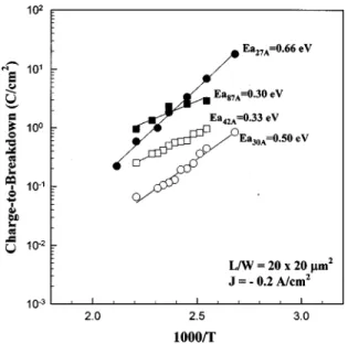
The temperature-accelerated oxide breakdown was stud-ied in detail. As shown in Fig. 2, the 50% Qbdvalues under
CCS injection are plotted against the reciprocal of absolute temperature ~i.e., 1/T! for four different oxide thickness splits. From the activation energy (Ea) of Qbd, as extracted
from the slope of the plot, the four curves can be roughly divided into two groups, i.e., those thicker or thinner than 4 nm. The activation energy increases by only 0.03 eV when oxide thickness decreases from 8.6 nm ~0.30 eV! to 4.2 nm
~0.33 eV!, indicating a very weak thickness dependence on activation energy. For oxide thinner than 4 nm, however, the activation energy shows a strong dependence on oxide thick-ness. Specifically, Ea increases to 0.5 and 0.66 eV for 3 and
2.7 nm oxides, respectively. Thus, despite the superior Qbd
for the 2.7 nm oxide at room temperature, Qbd becomes
worse than that of 8.7 nm oxide when the stress temperature is elevated above 150 °C. The accelerated temperature de-pendence on dielectric breakdown for scaled oxide may be ascribed to the increasing fraction of the structural transition layer ~STL! which is the structural imperfection due to the distorted Si–O4 tetrahedron network as a result of high stress/strain in the Si/SiO2 interface. In the STL, the exis-tence of suboxides (Si2O, SiO, and Si2O3) has been previ-ously identified to exist by x-ray photoelectron spectra.10,11 The built-in compressive strain in the Si–O bonds causes the reduction of the Si–O–Si average bond angle or the Si–Si second neighbor distance.10,12 In addition, the Si–H bond which results mainly from post-metal anneal in forming gas ambient and the stretched Si–O bond in the STL are pro-posed to be the precursor of oxide breakdown13 and is be-lieved to be responsible for the temperature dependence of oxide breakdown.3,14 It has been reported that the tempera-ture dependence of oxide breakdown can be ascribed to both atomic and molecular hydrogen diffusion released from Si–H bond breaking caused by the anode hole injection3,15 and that the presence of the compressive strain will lower the diffusion barrier of those hydrogen-related species.10 Since the STL thickness is approximately 1.0 nm for all oxides,10 the fraction of STL to gate oxide thickness will increase with scaling. Fourier transform infrared ~FTIR! spectroscopy measurements further indicated that the strain at the SiO2/Si interface indeed increases as oxide thickness decreases.14 Therefore, the temperature acceleration effect will be en-hanced for ultrathin oxides.
Figure 3 depicts the Arrhenius plot of oxide breakdown
FIG. 1. 50% charge-to-breakdown measured at 25 °C ~solid circle! and 180 °C ~open circle! under gate injection of 20.2 A/cm2as a function of
oxide thickness. The area of all capacitors is 431026cm2. Insert shows
typical V – t curves of charge-to-breakdown tests on 2.5 nm oxide at 25 and 180 °C.
FIG. 2. The temperature acceleration effects on charge-to-breakdown, Qbd.
The temperature is from 348 to 473 K. Activation energy Eais also given.
The stress current density is 0.2 A/cm2under gate injection.
FIG. 3. The temperature acceleration effects on breakdown field, Ebd. The
temperature is from 348 to 473 K. The polycrystalline silicon depletion effect is also taken into account. Activation energy Eais also given.
3709
Appl. Phys. Lett., Vol. 74, No. 24, 14 June 1999 Chenet al.
This article is copyrighted as indicated in the article. Reuse of AIP content is subject to the terms at: http://scitation.aip.org/termsconditions. Downloaded to IP: 140.113.38.11 On: Wed, 30 Apr 2014 08:31:15
field, extracted from ramped I – V measurements, for various oxide thicknesses as a function of temperature in the range 75–200 °C. Test transistors with gate area of 2310mm2 were stressed under substrate injection polarity ~i.e., 1Vg!
with source/drain grounded. The polycrystalline silicon depletion effect was taken into account while extracting the breakdown field. At first glance, it is in general agreement with the fact that increasing stress temperature is accompa-nied by decreasing breakdown voltage, regardless of oxide thickness. As has been mentioned previously, this is ascribed to the increasing interaction between tunneling electrons and the lattice at elevated temperature. The activation energy of breakdown field exhibits the same behavior as that of Qbd,
i.e., the activation energy of breakdown field increases mo-notonously with decreasing thickness. Because of the strong temperature degradation effect in ultrathin oxides, break-down field of the 2.5 nm oxide is lower than 4.2 nm oxide, while the breakdown field of the 3 nm oxide is lower than that of 8.7 nm oxide, when the stress temperature is raised above 150 °C.
Since the reliability of the 2.5 nm oxide exhibits such an enormous dependence on temperature, it was further ana-lyzed under different stress conditions. As depicted in Fig. 4, MOS capacitors with 2.5 nm oxide were stressed at different temperatures~i.e., 25 and 180 °C! under gate injection polar-ity with different stressing levels ~i.e., 0.2 and 1 A/cm2!. Some test capacitors also received a 2 C/cm2~at a stressing current density of 0.2 A/cm2! prestress at 180 °C before
sub-jected to the 0.2 A/cm2 stress until failure at 25 °C~circles!. As shown in Fig. 4, by increasing the stress level from 0.2 to 1 A/cm2, three orders magnitude in Qbd reduction is
ob-served. This is because under higher stress levels, the domi-nant tunneling process changes from direct tunneling~DT! to ~FN! tunneling, while electrons in the DT process typically deposit negligible energy in oxides. More importantly, our results also show that prestressing at elevated temperature for even a small stress level ~e.g., 2 C/cm2! can lead to signifi-cant Qbd reduction in subsequent stressing at room
tempera-ture. Such results indicate that the cumulative nature of Qbd is accelerated at high temperature stress. Hence, both tem-perature and stress level are important factors for Qbd. One can conclude that any low-level stressing experienced at high temperature during the real wafer fabrication process may cause significant degradation of oxide reliability in the com-pleted MOS devices with ultrathin oxide.
In summary, we have studied the accelerated effects of temperature on the breakdown characteristics of oxides as thin as 2.5 nm. It is shown that temperature-accelerated ox-ide breakdown is strongly aggravated for ultrathin oxox-ide. Therefore, more attention should be paid to real wafer pro-cessing steps that require elevated temperature in order to ensure that gate oxide integrity for ULSI devices employing ultrathin gate oxide is not jeopardized.
1B. E. Weir, P. J. Silverman, D. Monroe, K. S. Krisch, M. A. Alam, G. B.
Alers, T. W. Sorsch, G. L. Timp, F. Baumann, C. T. Liu, Y. Ma, and D. Huang, Tech. Dig. Int. Electron Devices Meet. 1997, 73~1997!.
2H. Iwai and H. S. Momose, Tech. Dig. Int. Electron Devices Meet. 1998,
163~1998!.
3
K. Eriguchi and M. Niwa, Appl. Phys. Lett. 73, 1985~1998!.
4
S. Ma, J. P. McVittie, and K. C. Saraswat, IEEE Electron Device Lett. 16, 534~1995!.
5C. F. Chen, C. Y. Wu, M. K. Lee, and C. N. Chen, IEEE Trans. Electron
Devices 34, 1540~1987!.
6
P. P. Apte and K. C. Saraswat, IEEE Trans. Electron Devices 41, 1595
~1994!.
7K. F. Schuegraf and C. Hu, IEEE Trans. Electron Devices 41, 1227 ~1994!.
8T. Brozekm, Y. D. Chan, and C. R. Viswanathan, IEEE Electron Device
Lett. 17, 288~1996!.
9H. C. Lin, M. F. Wang, C. C. Chen, S. K. Hsien, C. H. Chien, T. Y.
Huang, C. Y. Chang, and T. S. Chao, Proc. Int. Reliab. Phys. Symp. 312
~1998!. 10
K. Eriguchi, Y. Harada, and M. Niwa, Tech. Dig. Int. Electron Devices Meet. 1998, 175~1998!.
11T. Sorsch, W. Timp, F. H. Baumann, K. H. A. Bogart, T. Boone, V. M.
Donnelly, M. Green, K. Evans-Lutterodt, C. Y. Kim, S. Moccio, J. Ro-samilia, J. Sapjeta, P. Silvermann, B. Weir, and G. Timp, Symp. VLSI Tech. 222~1998!.
12S. Miayazaki, H. Nishimura, M. Fukuda, L. Ley, and J. Ristein, Appl.
Surf. Sci. 113/114, 585~1997!.
13D. Arnold, E. Cartier, and D. J. DiMaria, Phys. Rev. B 49, 10278~1994!. 14
H. Satake, N. Yasuda, S. Takagi, and A. Toriumi, Appl. Phys. Lett. 69, 1128~1996!.
15J. D. Bude, B. E. Weir, and P. J. Silverman, Tech. Dig. Int. Electron
Devices Meet. 1998, 179~1998!. FIG. 4. Cumulative charge-to-breakdown (Qbd) results for 2.5 nm oxide
stressed under four different conditions.
3710 Appl. Phys. Lett., Vol. 74, No. 24, 14 June 1999 Chenet al.
This article is copyrighted as indicated in the article. Reuse of AIP content is subject to the terms at: http://scitation.aip.org/termsconditions. Downloaded to IP: 140.113.38.11 On: Wed, 30 Apr 2014 08:31:15