國立交通大學
材料科學與工程研究所
博士論文
應用於毫微米波段高電子遷移率電晶體
之覆晶封裝研究
Flip-chip Packaging Structure of HEMTs Devices for
Millimeter-wave Applications
研 究 生:王景德
指導教授:張翼 博士
應用於毫微米波段高電子遷移率電晶體
之覆晶封裝研究
Flip-chip Packaging Structure of HEMTs Devices for Millimeter-wave
Applications
研 究 生:王景德 Student:Chin-Te Wang
指導教授:張翼 博士 Advisor:Dr. Edward Yi Chang
國立交通大學
材料科學與工程研究所
博士論文
A Dissertation
Submitted to Department of Materials Science and Engineering College of Engineering
National Chiao Tung University In Partial Fulfill of the Requirements
For the Degree of
Doctor of Philosophy in Engineering 2014
Hsinchu, Taiwan
i 應用於毫微米波段高電子遷移率電晶體之覆晶封裝研究 研究生:王景德 指導教授:張 翼 博士 國立交通大學材料科學與工程研究所 摘要 近年來,無線通訊與成像技術的快速發展,推動其頻率源朝向毫微米與次毫 微米波段,較大的傳輸頻寬、高傳輸速度與高解析度為這些頻率波段良好的特性, 為了實現這些應用,封裝技術扮演了非常重要的角色,不僅提供了晶片與基板的 傳輸途徑,還提供了散熱與保護的功能。在毫米波段的晶片層級封裝上,覆晶封 裝為受到注目的技術,與傳統的打線接合比較,覆晶封裝的優點包含了較短的轉 接路徑來減少寄生效應、較高的生產效率以及更小的封裝尺寸。 本論文探討應用於毫微米波段之覆晶封裝。首先,砷化鎵銦高電子遷移率電 晶體封裝於氧化鋁基板上,在 60GHz 量測結果,藉由最佳化的覆晶轉接,覆晶 封裝前後的元件特性幾乎相同。此外,利用微波積體電路概念設計並製作 60GHz 兩階增益器,來驗證覆晶封裝元件設計 V-band 電路的可行性,將高電子遷移率 電晶體封裝於設計有匹配電路的氧化鋁基板上,在 60GHz 時此增益器呈現 9dB 的小訊號增益,從結果顯示此微波積體電路的概念於毫微米波段的可行性。此外, 由於晶片與基板的熱膨脹係數的不匹配會產生熱應力,而導致封裝結構的損壞, 利用 BCB 當做底膠填充的材料來增加覆晶結構的機械強度與可靠度,從 100GHz 量測結果中,擁有較好的介電特性的 BCB 表現出優於傳統環氧樹脂底膠填充的 高頻特性,從熱循環測試與剪切力測試的結果,BCB 的填充可以有效的提升覆 晶封裝結構的可靠度。 利用直接覆晶封裝(FCOB)於第二層的基板而省略晶片層級的封裝,在未
ii 來毫微米波應用達成兼顧成本效應與良好特性,商用的 RO3210 高分子基板因為 有與氧化鋁基板相近的介電特性為有潛力的基板材料,封裝在高分子基板上的元 件搭配經過最佳化的覆晶轉接直到 W-band 呈現良好的特性,利用最佳化的封裝 結構,封裝元件仍擁有低雜訊且良好的增益特性,同時環氧樹脂底膠填充有效增 加高分子覆晶結構的可靠度且沒有明顯的特性損耗。此外,也探討覆晶封裝製程 中的溫度對封裝元件特性的影響,從實驗中可以發現較高的接合溫度會產生高頻 特性的損耗,主要的原因是覆晶結構中砷化鎵晶片與高分子基板的熱膨脹係數不 同所產生的熱應力,且利用有效電路模型,從 S 參數中萃取出的寄生電阻電容數 值中可以發現,較高的接合溫度有較高的數值,因此,合理的覆晶接合條件可以 減少熱應力並保持良好特性。
iii
Flip-chip Packaging Structure of HEMTs Devices for
Millimeter-wave Applications
Student: Chin-Te Wang Advisor: Dr. Edward Yi Chang
Department of Materials Science and Engineering National Chiao-Tung University
Abstract
In recent years, the rapid development for wireless communication and imaging system has pushed the operational frequency for wireless communication to millimeter-wave or sub millimeter-wave bands. These frequency bands have several advantages, including wide transmission bandwidth, high transmission speed, and high signal resolution. In order to realize the targeted applications, the packaging technology plays an important role to provide the transmission path from chip to substrate, the heat dissipation, environment protection. In the chip-level packaging, the flip-chip is the more promising approach for millimeter-wave applications in comparison with conventional wire bonding. The advantages of the flip-chip interconnection are short path to reduce the parasitic effect and compact product size.
This dissertation presents the study on the flip-chip packaging structure of HEMT devices for millimeter-wave applications. The flip-chip packaged In0.7Ga0.3As
MHEMT device was firstly demonstrated on Al2O3 substrate. By adopting the
optimized design for the flip-chip transition, the packaged device shows almost similar RF performance as the bare die up to 60 GHz. In addition, a two-stage gain block at 60 GHz was designed and fabricated using the microwave integrated circuit
iv
(MIC) approach to demonstrate the applicability for V-band applications. The MHEMT device was flip-chip packaged on Al2O3 substrate with the matching circuit.
The gain block exhibited a small signal gain of 9 dB at 60 GHz, indicating the feasibility of MIC approach for millimeter-wave applications. The thermal stress induced by the coefficient of thermal expansion (CTE) mismatch between the chip and the substrate can distort the flip-chip structure. BCB material was used as the underfill to improve the reliability and mechanical property of the flip-chip structure. The good dielectric property of BCB exhibited better RF characteristics up to 100 GHz as compared to the conventional epoxy-based underfill. From the results of thermal cycling test and shear force test, BCB underfill can effectively improve the reliability of the flip-chip structure.
The flip-chip on board (FCOB) technology bypassed the chip-level package to achieve cost-effective millimeter-wave package. The RO 3210 polymer substrate was the promising substrate because its dielectric property is similar to Al2O3 substrate.
The packaged device with the optimal flip-chip structure exhibited good RF results up to W-band. An exopy-based underfill was applied to improve the reliability without the characteristic degradation of the device. Analytical results revealed that the proposed packaging structure maintained a low minimum noise figure of 3 dB with 6 dB of associated gain at 62 GHz. In addition, the impact of bonding temperature on the device performance was also investigated. The degradation in RF performance was observed at higher bonding temperature. The reason of the degradation was mainly due to the mismatch in the CTE between the GaAs chip and the polymer substrate. From the equivalent circuit extraction from S-parameter measurements, the higher parasitic values occurred during the higher bonding temperature. The applicable bonding condition could reduce the thermal stress without degrading the RF performance.
v 致謝 博士班生涯隨著畢業論文完成而有個完美的結束。首先,感謝我的指導教授 張翼博士,提供機會讓我進入高頻複合物半導體的研究領域,在老師的教導下, 進行有邏輯的實驗與研究,訓練我獨立思考與解決問題的能力,實驗室提供完善 的實驗儀器與量測設備,讓我有豐富的實作經驗與能力。有機會參與經濟部學界 科專三年計畫,接觸到不同科系專長的教授與博士生拓展學識,並學會與人合作 與溝通的技巧。老師給予我許多機會參與國際研討會,藉此開闊視野並吸收研究 領域上的新知,並鼓勵我申請國科會三明治計劃到德國柏林 FBH 研究機構交換 學生一年,這些經歷充實我的博士班生活。 其次,我特別感謝 Flip-Chip 組的吳偉誠學長、許立翰學長、黃珍嬅學姐與 胡吟竹學姐,感謝他們在我新進實驗室時,指導我實驗的方向與技巧,在學業與 生活上給予我許多寶貴的意見與幫助,感謝吳偉誠學長與許立翰學長給予我在論 文寫作上的想法與意見,還有胡志偉同學與我一同作實驗並且總是給我正向的意 見。還有感謝元智大學許恆通博士與郭建億學長指導我分析實驗資料與討論論文 投稿,讓我順利完成博士班論文。 在博士班生涯中,李哲倫先生、林岳欽學長、吳雲驥學長、黃瑞乾學長、呂 宗育學長、張家達學長、林龔樑學長、黃延儀學長與、林美璇學姐給予許多實驗 與量測上的指導,還要感謝江韵涵小姐、游宏偉同學、黃偉進同學、蕭佑霖同學、 蔡思屏同學、邱昱盛同學、許青翔同學、蘇詠萱同學、林瑞琴同學、吳青峰同學、 詹前樟先生黃碧玉小姐、李芳茗先生等的幫忙。 最後,我要特別感謝我的父母的支持與鼓勵,讓我能夠專心順利完成學業, 還有重要的女友琳婷,謝謝她的體諒與相伴讓我的博士班生活充滿活力,願這份 榮耀與您們分享。
vi
Contents
Abstract (in Chinese)………...……….….…i
Abstract (in English).………..iii
Acknowledge (in Chinese) ……….……..v
Contents………....vi
Table Captions………...……….…..ix
Figure Captions……….x
Chapter 1 Introduction……….1
1.1 Millimeter-Wave Application………...……….1
1.2 Monolithic Microwave Integrated Circuits (MMICs) and Microwave Integrated Circuits (MICs) ………2
1.3 Microwave Packaging Structure………...………3
1.3.1 RF Performance Optimization of the Flip-Chip Structure………...4
1.3.2 Mechanical Property Improvement of the Flip-Chip Structure………5
1.4 Challenges of Microwave Flip-Chip Packaging………...……….7
1.5 Outline of this Dissertation………8
Chapter 2 The Fabrication Process of the Flip-Chip Structure……….22
2.1 Fabrication of Flip-chip Substrate………..………...…22
2.2 Fabrication of Flip-Chip Bonding Process………..….…..23
2.3 Underfill Process of the Flip-chip Substrate………..………23
2.4 No-flow Underfill process for Flip-chip Structure……….24
vii
Chapter 3 A Flip-Chip Packaged InGaAs MHEMT Device on A12O3 Substrate for
Millimeter-Wave Low-Noise Applications………...……30
3.1 Background and Motivation………...…31
3.2 Fabrication and Flip-Chip Package Process.……….……….32
3.3 Measured Results of the Packaged MHEMT on Al2O3 Substrate………..33
3.4 V-Band Flip-Chip Assembled Gain Block using 150 nm In0.6Ga0.4As MHEMTs Technology……….35
3.5 Summary………37
Chapter 4 Investigation of the Flip-chip Package with BCB Underfill for W-band Applications………47
4.1 Background and Motivation………...……47
4.2 Fabrication and Flip-Chip Package Process………..……….…49
4.3 Measured Results of the Flip-Chip Packaging Structure with underfill Injection….50 4.4 Reliability Test Results of the Flip-Chip Packaging Structure with underfill Injection………...……….…..52
4.5 Summary………53
Chapter 5 Flip-Chip Packaging of Low-Noise Metamorphic High Electron Mobility Transistors on Low-Cost Organic Substrate………...62
5.1 Background and Motivation………..………….63
5.2 Fabrication and flip-chip package process……….64
5.3 Design and Optimization of the flip-chip packaging structure on RO 3210 polymer substrate……….66
5.4 Assessment of Thermal Impact on Performance of MHEMT Devices on RO 3210 Polymer Substrates ………...…….67
viii
5.6 Summary………71
Chapter 6 Conclusions………..…….…….88
References………90
Curriculum Vitae (in English) ………..……98
ix
Table Captions
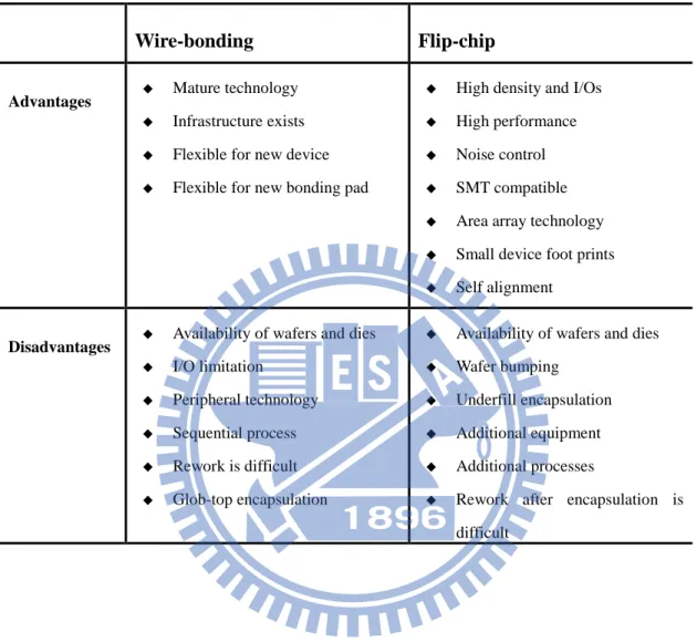
Chapter 1
Table 1.1 Comparison between wire-bonding and flip-chip technologies………..…20 Table 1.2 Material properties of the substrates commonly used for flip-chip packaging…....21
Chapter 4
Table 4.1 Material properties of underfills………..…….54 Table 4.2 Shear force test results………..………61
Chapter 5
Table 5.1 Material properties of the substrates commonly used for flip-chip packaging…….87 Table 5.2 Bonding conditions at high and low substrate bonding temperatures………..87 Table 5.3 Extracted parasitic values at high and low bonding temperatures………87
x
Figure Captions
Chapter 1
Figure 1.1 (a) The image and (b) the electric characteristic of monolithic F.E.T. amplifier chip
at frequency up to X-band……….10
Figure 1.2 (a) Circuit diagram and (b) measured and simulated frequency characteristics of 60 GHz two-stage cascade amplifier………...11
Figure 1.3 The conventional microwave packaging structure………...12
Figure 1.4 The image of the wire-bonding interconnection………...13
Figure 1.5 The image of (a) flip-chip structure and (b) flip-chip bumps..………..……...14
Figure 1.6 Optimized interconnect design. (a) Layout on the motherboard without any compensation. (b) On chip compensation: staggered bumps on the center conductor. (c) On substrate compensation: single high-impedance (Hi) line section at the interconnect and the high–low (Hi–Lo) version………....………..……...15
Figure 1.7 Optimized design of a flip-chip interconnect by means of compensation: simulated reflection loss as a function of frequency between no compensation, staggered bumps design and on substrate Hi compensation design………....………..……...16
Figure 1.8 The conventional flip-chip process with underfill injection. ………..……...17
Figure 1.9 Comparison of measured (a) reflection loss (S11) and (b) insertion loss (S21) of flip-chip structure with and without epoxy underfill material………...18
Figure 1.10 S-parameters comparison of flip-chip packaged (a) 30 GHz and (b) 60 GHz LNAs with and without underfill material………19
Chapter 2 Fig. 2.1 The in-house fabrication process of the Al2O3 substrate………...…….……..26
Fig. 2.2 The image of the M9 flip-chip bonder………..27
Fig. 2.3 The in-house process of epoxy resin injection………..…...28
Fig. 2.4 The SEM cross section view of the flip-chip structure with underfill. ………....28
xi
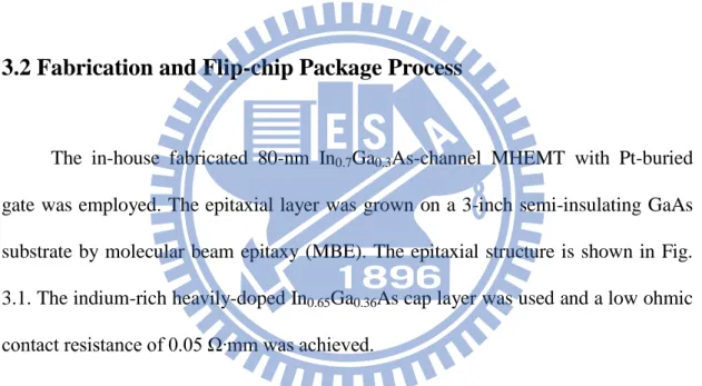
Chapter 3
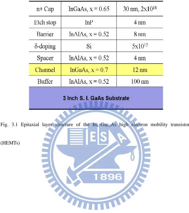
Fig. 3.1 Epitaxial layer structure of the In0.7Ga0.3As high electron mobility transistors (HEMTs)………...38 Fig. 3.2 (a) Image of the in-house fabricated 80-nm gate In0.7Ga0.3As MHEMT device, (b) The
SEM image of the electroplated micro Au bumps (c) The schematic of the flip-chip packaged structure (d) Image of the flip-chip packaged In0.7Ga0.3As MHEMT device on Al2O3
substrate. ………...39 Fig. 3.3 In-house fabrication flow of the alumina (Al2O3) substrate for flip-chip packaging
structure………....40 Fig. 3.4 Comparison of drain-source current (IDS) versus drain-source voltage (VDS) curves
with various gate voltages (VG) of In0.7Ga0.3As MHEMT devices with and without flip-chip
packaging..……….………...41 Fig. 3.5 Comparison of drain current density (IDS) and transconductance (gm) as a function of
gate-source voltage (VGS) at VDS = 1.3V for In0.7Ga0.3As MHEMT devices with and without
flip-chip packaging..…….………...42 Fig. 3.6 Comparison of insertion gain (S21) and reflection loss (S11) for In0.7Ga0.3As MHEMT
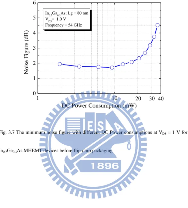
devices with and without flip-chip packaging..………...43 Fig. 3.7 The minimum noise figure with different DC Power consumptions at VDS = 1 V for
In0.7Ga0.3As MHEMT devices before flip-chip packaging………...44
Fig. 3.8 Comparison of the minimum noise figure and associated gain at VDS = 1.0 V, VG =
-0.1 V for In0.7Ga0.3As MHEMT devices with and without flip-chip packaging………..45
Fig. 3.9 Circuit diagram of the two-stage gain block designed at 60 GHz..……….46 Fig. 3.10 Measured S-parameters of the fabricated gain block biased at VDS = 0.5 V and VGS =
0.4 V....……….……….46
Chapter 4
Fig. 4.1 (a) A schematic and (b) an SEM image of the cross section of the flip-chip structure with BCB underfill injection……….…55 Fig. 4.2 The design parameters for the flip-chip structure with BCB injection…………...56 Fig. 4.3 The no-flow underfill process flow for flip-chip structure…………...57
xii
Fig. 4.4 Measured S-parameters of the flip-chip interconnects without UF and with BCB or epoxy underfill injection………...58 Fig. 4.5 LM(Gold), LC(GaAs) and LS(Al2O3) of the flip-chip interconnect structure as extracted from
EM simulation; the LBCB and LEpoxy as extracted from the measurement for comparison…….59
Fig. 4.5 Thermal cycling test results of the flip-chip interconnect with and without BCB underfill injection………..60
Chapter 5
Fig. 5.1 (a) Schematic and (b) cross-sectional views of the flip-chip interconnect structure...73 Fig. 5.2 In-house fabrication of FCOB structure on RO 3210 polymer substrate...74 Fig. 5.3 SEM images of the low-cost RO 3210 organic substrate (a) before and (b) after CMP lapping process………..…75 Fig. 5.4 Simulated and measured results of the CPW transmission lines on low-cost organic substrate………..………...76 Fig. 5.5 (a) Measured S-parameter of the common flip-chip interconnect structure and (b) Smith chart of the corresponding S11 results…..………..…………....77 Fig. 5.6 (a) Schematic and (b) simulation results of the compensation design in flip-chip interconnect structure…..………..…………...78 Fig. 5.7 Measured S-parameter results of the optimized flip-chip interconnect structure with and without underfill..…..………..…………...79 Fig. 5.8 Measured drain current and DC transconductance as functions of gate bias at VDS =
0.5 V of the flip-chip-packaged device under different bonding conditions, (a) with high bonding temperature and (b) with low bonding temperature, with those of bare dies included for comparison...………...………80 Fig. 5.9 Measured MSG/MAG as a function of frequency for the cases of bare die, flip-chip-packaged device with high bonding temperature, and flip-chip-packaged device with low bonding temperature………...81 Fig. 5.10 Illustration of induced mechanical stress during bonding process with different bonding temperatures………...82
xiii
Fig. 5.11 The corresponding equivalent circuit model of the bump interconnect……….82 Fig. 5.12 Measured and modeled S parameters of the complete structure in Fig. 6 at high bonding temperature………..83 Fig. 5.13 Comparison of drain current density (IDS) and transconductance (gm) as a function of gate-source voltage (VGS) at VDS = 0.8 V between the In0.6Ga0.4As mHEMT device, packaged device, and packaged device with underfill ……….84 Fig. 5.14 Comparison of insertion gain (S21) between the In0.6Ga0.4As MHEMT device, packaged device, and packaged device with underfill………..…………...85 Fig. 5.15 Comparison of the minimum noise figure and associated gain at VDS = 0.8 V, VG =
-0.6 V between the In0.6Ga0.4As MHEMT device, packaged device, and packaged device with
1
Chapter 1
Introduction
1.1 Millimeter-Wave Applications
In recent years, the rapidly growing demands on the wireless communication, consumer electronics and imaging systems to cutting edge scientific applications have pushed the operating frequency to millimeter-waves (MMWs) range or beyond (sub-MMWs)[1-7]. These operating frequencies bands are very attractive due to the wide data bandwidth, high transmission speed and high signal resolution. The other significant benefit of MMWs band is the more compact size of RF components. The lower wavelength at higher frequencies allows high density, small size circuit and module designs. Nowadays, the development of the 60 GHz wireless communication becomes more and more popular in the market [8]. The 60 GHz technology provides very high speed of the point to point wireless transmission because the signal is easily absorbed by oxygen [7]. Besides, the MMWs and sub-MMWs are the potential frequency sources for security and medical imaging systems. The promising applications include the detection of concealed weapons under clothing [1-7]. Such applications have also accelerated the development of device fabrication as well as the packaging technologies to meet the stringent requirements for MMWs and sub-MMWs operations.
2
1.2 Monolithic Microwave Integrated Circuits (MMICs) and
Microwave Integrated Circuits (MICs)
To realize these MMWs and sub-MMWs applications, the development of the transmitter and receiver modules is critical to guarantee the desired system performance. The key technical challenges are providing broadband gain and low noise figure in receiver design. The transmitter design needs to handle high output gain at high frequencies. There are two main approaches to develop the microwave circuits for transmitter and receiver modules: monolithic microwave integrated circuits (MMICs) and microwave integrated circuits (MICs).
MMICs combine the active components, passive components and interconnections, which are fabricated simultaneously on the same semiconductor substrate [9-13]. The MMIC fabrication on the same substrate at the same time not only saves the unit cost but also reduces the device size and weight. Besides, the characteristics from MMIC to MMIC are more uniform with better performance due to less parasitic effects. In 1975, Pengelly and Turner firstly demonstrated the MMIC amplifier at X-band. As shown in Fig. 1.1, their X-band boardband amplifier included field-effect transistor (FET), capacitors, and inductors on the same GaAs chip, which exhibited the boardband performance of 4.5 dB over 7.5 GHz to 11.5 GHz [9]. Hung
et al. built the first mm-wave MMIC at Ka-band. The MMIC provides stable power
gain with near 0.5 W of output at 28 GHz [10].
Compared to MMICs, MICs have several benefits such as low cost of process development, flexible design and high production yield [14-15]. The different
3
semiconductor device technologies, including MESFETs, bipolar, diodes, digital, etc., can be flexibly combined on the same carrier. The design with the passive components fabricated on the substrate side not only reduces the process complexity but also avoids the parasitic effect between the active and passive components. Besides, the selected device with acceptable characteristics can effectively increase the production yield. Sakai et al. demonstrated the 20 GHz single-stage and two-stage amplifiers on Si substrate using MIC design. The micro bump bonding was used to connect the HEMT and HBT active devices to input and output matching circuit on Si substrate [14]. In 1997, Arai et al. designed the two-stage amplifier and frequency-doubler at 60 GHz with flip-chip packaged pHEMT [15]. From Fig. 1.2, the good agreement between simulated and measured results shows the potential of the MIC approach for future MMWs applications.
1.3 Microwave Packaging Structure
Figure 1.3 illustrates the conventional microwave packaging structure, which includes three packaging levels: chip or ICs to substrate, substrate to printed-circuit board (PCB), and PCB to motherboard. The transitions between each level provide transmission path with low loss and good reliability [16]. The wire-bonding is the mature technology to connect an IC to another electronic devices or PCB in the industry, as shown in Fig. 1.4 [17-21]. The common bond-wire materials are gold (Au) and aluminum (Al). When higher operating frequencies, wire-bonding technology becomes inappropriate because the parasitic effect due to the long interconnection. Thus, the flip-chip technology is applied to MMWs applications due to its short
4
interconnect length, good thermal management, better mechanical stability and small package size [22-34]. Figure 1.5 shows the flip-chip structure and bumps. The chip is mounted on the substrate in face-down manner so that the shorter interconnection length from chip to substrate can be achieved to reduce the parasitic effect at higher frequencies. Table 1.1 lists the characteristics of the wire-bonding and flip-chip bonding. The bump is the interconnection to transmit signal from substrate to chip and chip to substrate. Hence, the major concerns of the flip-chip technology for MMWs applications are high frequency performance and mechanical property. The following sections will discuss these characteristics of the flip-chip transition.
1.3.1 RF Performance Optimization of the Flip-Chip Structure
The performance degradation at higher operating frequencies is mainly due to the change of the characteristic impendence around the flip-chip transition. According to previous studies, the factors affect the RF performance had been investigated and established [29-35]. The factors included bump height, bump pad area (length and width), dielectric overlap between chip and substrate and width between the signal bump and ground bump. The detuning effect is the important issue of the flip-chip structure because the distance between the face-down chip and substrate changes the electrical characteristics of the chip circuit. To suppress the undesired effect, the bump height should be larger than about 0.3 of coplanar waveguide (CPW) transmission line ground-to-ground distance [27,28]. Besides, the bump pad area and dielectric overlap should be as small as possible to minimize the reflection loss from the capacitance change around the interconnection. The larger width between signal
5
bump and ground bump can improve the return loss due to an internal compensation effect. In order to further improve the MMWs performance, there are two main solutions to compensate by reducing the excess capacitance at flip-chip transition as shown by Fig. 1.6. One is on the chip side by staggering signal bump and ground bumps. The field around the signal bump is in the air so that the capacitance value can be reduced. The other one is on the substrate side by adding the high impendence line next to the flip-chip transition. Figure 1.7 shows the simulation results between without compensation, staggering bump, and high impendence line. The return loss can be effectively improved by using these compensation designs. The disadvantage of the compensation design on chip is the additional chip area and not compatible with common chip design; however, the compensation design on substrate side is easy process and cost effectiveness approach to optimize the flip-chip transition.
1.3.2 Mechanical Property Improvement of the Flip-Chip Structure
In the flip-chip structure, the signal transmission is attached by flip-chip bump interconnections. The chip and the substrate are connected by several bumps since the mechanical property of the flip-chip transition should be considered carefully. The CTE mismatch is the major concern of the flip-chip interconnection structure. During the thermal cycling, the thermal stress occurs in the flip-chip transition due to the CTE mismatch and then fractures the flip-chip transitions. To improve the mechanical property and reliability of the flip-chip transition, the use of underfill is the potential approach because it can restrict and redistribute the stress between bumps, chip, substrate and underfill. The underfill can increase the bump fatigue life by 10 to 100
6
times. [36]
The epoxy-based resin underfill has been widely used for some low frequency applications in the industry. The dielectric constant and dielectric loss of the epoxy-based resin underfill are 3.5 (at 10 MHz) and 0.02 (at 10 MHz), respectively. Figure 1.8 shows the conventional flip-chip process with underfill injection. [36] After the flip-chip bonding process, the liquid underfill is injected into the gap between chip and substrate by capillary force. Figures 1.9 (a) and 1.9 (b) show the comparison between the flip-chip structure with and without underfill injection. [37] The return loss and insertion loss of the flip-chip structure with underfill were increased. The flip-chip packaged 30 GHz and 60 GHz low noise amplifier MMICs with underfill injection shift the frequency response of 3 dB and 9 dB, as shown in Figure 1.10 [38]. It has been reported that the impact of underfill injection on RF performance is due to the change of the characteristic impendence between the chip and the substrate [36-39]. Besides, the extra dielectric loss was induced by the underfill material because its dielectric is larger than the air. After re-optimizing the dimension of the chip transmission line to 50 Ω , the flip-chip structure with epoxy-based underfill exhobits the similar RF performance to flip-chip structure without underfill [40].
1.4 Challenges of Microwave Flip-Chip Packaging
According to previous studies, the flip-chip interconnect has been successfully demonstrated to package some device and MMICs [ ]. The flip-chip interconnect exhibited good high frequency performance. However, the rapidly growing demands
7
on the data bandwidth and transmission speed of modern wireless communication systems have pushed the operating frequencies to MMWs range or beyond [6-8]. It also accelerates the development of device fabrication as well as packaging technologies to meet the stringent requirements for high-frequency operations. On the device side, mHEMT technology with indium (In)-rich channels has been attractive due to the very high electron mobility and saturation velocity of InGaAs materials [41-44].
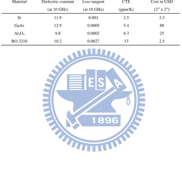
The development of packaging configuration and interconnect technologies has become critical since both high performance and cost effectiveness are the main themes of modern applications. The flip-chip-on-board (FCOB) technology is a very cost-effective solution for high-frequency applications because it bypasses the chip-level assembly, which makes it easier for further integration with other components in the system [45-48]. Therefore, such technology not only reduces RF loss but also saves the material cost by eliminating of the chip level package. Table 1.2 lists the material properties of some conventional substrates for MMWs applications. Clearly, the commercial RO 3210 organic substrate from Rogers CorporationTM is a good candidate due to its very low cost with comparable material properties at high frequencies. Giesler et al. and O'Malley et al. had successfully demonstrated the flip-chip structure on FR4 organic substrate by using 97Pb/3Sn solder bump interconnection and the reliability improvement of the flip-chip interconnect with encapsulation [45,46]. Hsu et al. demonstrated the flip-chip structure on the RO 3210 organic substrate with epoxy-based underfill to work up to 50 GHz and pass the 600-cycle thermal-cycling test [48].
8
the development of the new underfill material with good dielectric property and dielectric loss is essential. Besides, the underfill materials should also have the characteristics of low moisture absorption, high thermal conductivity, good mechanical strength, and good adhesion to the chip and substrate materials.
1.5 Outline of this Dissertation
This dissertation presents the study on flip-chip packaging for MMWs applications.
Chapters 2 presents the in-house flip-chip fabrication process, including the fabrication process of flip-chip bonding and underfill injection.
In Chapter 3, a flip-chip 80-nm In0.7Ga0.3As MHEMT device on an alumina
(Al2O3) substrate with very little degradation on device RF performance up to 60 GHz
is firstly presented. As compared to the bare chip, the packaged device exhibited very small degradation in performance. Besides, a two-stage gain block at 60 GHz was designed and fabricated using the MIC approach to demonstrate the applicability of such device for V-band applications.
In Chapter 4, Benzocyclobutene (BCB) was used as the underfill in this study to improve the mechanical strength and reliability of the flip-chip package using the no-flow process and provided good RF performance up to 100 GHz with a lower dielectric loss. The thermal cycle and shear force tests show that the underfill injection can significantly improve the reliability of a flip-chip package.
In Chapter 5, the in-house fabricated In0.6Ga0.4As mHEMT device was
9
technology. An exopy-based underfill was applied to improve the reliability with almost no degradation of the electrical characteristics up to 60 GHz. Besides, the impact of bonding temperature on the device performance was also experimentally investigated through equivalent circuit extraction from S-parameter measurements. Such degradation was mainly due to the thermal-mechanical stress resulting from the mismatch in CTE between the GaAs chip and the polymer substrate.
10
(a)
(b)
Fig. 1.1 (a) The image and (b) the electric characteristic of monolithic F.E.T. amplifier chip at frequency up to X-band [9].
11
(a)
(b)
Fig. 1.2 (a) Circuit diagram and (b) measured and simulated frequency characteristics of 60 GHz two-stage cascade amplifier [15].
12
13
14
(a)
(b)
15
Fig. 1.6 Optimized interconnect design. (a) Layout on the motherboard without any compensation. (b) On chip compensation: staggered bumps on the center conductor. (c) On substrate compensation: single high-impedance (Hi) line section at the interconnect and the high–low (Hi–Lo) version [31].
16
Fig. 1.7 Optimized design of a flip-chip interconnect by means of compensation: simulated reflection loss as a function of frequency between no compensation, staggered bumps design and on substrate Hi compensation design [31].
17
18
(a)
(b)
Fig. 1.9 Comparison of measured (a) reflection loss (S11) and (b) insertion loss (S21)
19
(a)
(b)
Fig 1.10 S-parameters comparison of flip-chip packaged (a) 30 GHz and (b) 60 GHz LNAs with and without underfill material [38].
20
Table 1.1 Comparison between wire-bonding and flip-chip technologies
Wire-bonding Flip-chip
Advantages Mature technology
Infrastructure exists
Flexible for new device
Flexible for new bonding pad
High density and I/Os
High performance
Noise control
SMT compatible
Area array technology
Small device foot prints
Self alignment
Disadvantages Availability of wafers and dies
I/O limitation
Peripheral technology
Sequential process
Rework is difficult
Glob-top encapsulation
Availability of wafers and dies
Wafer bumping
Underfill encapsulation
Additional equipment
Additional processes
Rework after encapsulation is difficult
21
Table 1.2 Material properties of the substrates commonly used for flip-chip packaging.
Material Dielectric constant (at 10 GHz) Loss tangent (at 10 GHz) CTE (ppm/K) Cost in USD (2” x 2”) Si 11.9 0.001 2.5 2.3 GaAs 12.9 0.0005 5.4 88 Al2O3 9.8 0.0002 6.3 25 RO 3210 10.2 0.0027 13 2.5
22
Chapter 2
The Fabrication Process of the Flip-chip Structure
The in-house fabrication process of the flip-chip structure was developed in the Compound Semiconductor Laboratory (CSDLab), National Chiao-Tung University (NCTU). The details of the substrate fabrication and flip-chip bonding process are described in this chapter.
2.1 Fabrication of Flip-chip Substrate
The conventional substrate material for MMWs application is Al2O3 substrate
because it has good dielectric properties with dielectric constant of 9.8 and dielectric loss of 0.0006 for high frequency applications. Besides, the small difference of CTEs between Al2O3 substrate (CTE~7 ppm/oC) and GaAs chip (CTE~5.8 ppm/oC) can
minimize the thermal stress inside the flip-chip structure during the temperature variation.
Figure 2.1 shows the in-house fabrication process of the Al2O3 substrate. First,
the seed layers of titanium (Ti) and Au metal (300 Å and 500 Å ) were sequentially deposited by E-gun evaporator onto the Al2O3 substrate to form the continuous layers
for the following electroplating process. Ti was used as the adhesion layer between the substrate surface and the following Au metal. The thin photoresist form Shipley Company was coated and patterned for the following Au electroplating of the CPW transmission lines. The thickness of the CPW transmission line was 3 μm. After that,
23
the thick photoresist from TOK Company was used and patterned for the Au bump position and profile. The double coating process of thick photoresist was used to achieve enough height of the flip-chip bumps. The bump diameter was 50 μm. During the electroplating of Au bumps, the electroplating current density and electroplating time were important parameters to control the bump height. The height of the Au bump was around 30 μm to avoid the undesired detuning effect. Final step was the removal of the seed layers of Au and Ti with the KI/I2 solution and dilute HF solution.
2.2 Fabrication of Flip-chip Bonding Process
After finishing the substrate process, the HEMT device and the passive transmission line were flip-chip bonded on the fabricated substrate by Au-to-Au thermal compression bonding process using M9 flip-chip bonder. Figure 2.2 shows the photograph of the flip-chip bonder. The bonding conditions, such as bonding temperature, bonding force and bonding time were optimized to achieve good interconnection between chip and substrate without significant loss. The bonding temperature on the chip side and the substrate side were 180 ℃ and 300 ℃, respectively. The bonding force was 10 grams per bump and maintained about 3 minutes.
2.3 Underfill Process of the Flip-chip Structure
The underfill was used to improve the reliability of the flip-chip interconnections because the connections between the chip and substrate are just some small Au bumps with 50 um of the diameter. The RF performance of the flip-chip structure with
24
underfill injection will be changed due to the change of the characteristic impendence. Hence, the epoxy resin (dielectric constant~3.5; dielectric loss~0.02) was studied the impacts of the underfill on electrical and mechanical properties.
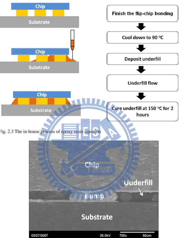
The in-house process of epoxy resin injection is shown in Fig. 2.3. First, the chip and the substrate were heated to 180 ℃ and 300 ℃ on M9 flip-chip bonder, respectively. After finishing the flip-chip bonding process, the sample was cooled down to 90 ℃ and then the epoxy resin was injected into the gap between chip and substrate by using the capillary force. When the underfill completely flowed to another side, a curing process at 150 ℃ for 2 hours was performed to make cross-linking of the polymer chains. Figure 2.4 shows the cross section view of the flip-chip structure with underfill. The image exhibits that the underfill successfully flowed into the gap between the chip and the substrate.
2.4 No-flow Underfill process for Flip-chip Structure
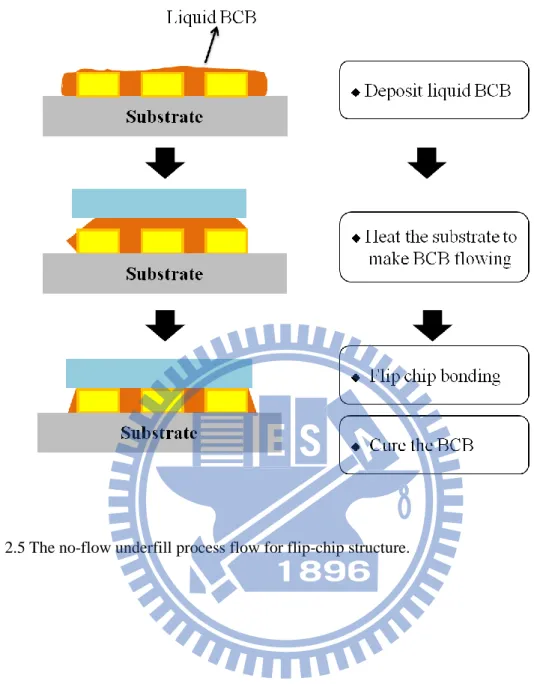
According the experiment result, liquid BCB cannot easily flow into the gap between the chip and substrate using capillary force. The BCB can’t be fully filled into the gap between chip and substrate. To solve this issue, the no-flow underfill process was proposed as shown in Fig. 2.5. Liquid BCB was first deposited on the substrate. Then the substrate was heated to cause BCB to flow. The heating conditions, such as the heating time and temperature, were optimized to enhance the BCB flow. Finally, the chip and the substrate were flip-chip bonded by using the Au-to-Au thermo-compression method. An additional curing at 250 ℃ for 2 hours was performed to facilitate cross-linking of the BCB polymer chains.
25
2.5 Scattering Parameter Measurement
Scattering Parameters (S-parameter) are fundamental to microwave measurement. These parameters were defined by the small signal gain and input/output emittance properties of any linear two port network [49].
The S-parameter measurement was characterized from 2 to 110 GHz by using an HP 8510XF network analyzer with E7352 test heads calibrated by using a standard load-reflection-reflection-match (LRRM) method.
26
Fig. 2.1
27
28
Fig. 2.3The in-house process of epoxy resin injection
29
30
Chapter 3
A Flip-chip Packaged InGaAs MHEMT Device on A1
2O
3Substrate
for MMWs Low-Noise Applications
In this chapter, a flip-chip 80-nm In0.7Ga0.3As MHEMT device on an Al2O3
substrate with very little degrade on device RF performance up to 60 GHz is firstly presented. After the flip-chip packaging, the device exhibited high IDS = 435 mA/mm
at VDS= 1.5 V, high gm= 930 mS/mm at VDS= 1.3 V. And the measured gain was 7.5
dB and the minimum noise figure (NFmin) was 2.5 dB at 60 GHz. As compared to the
bare chip, the packaged device exhibited very small degradation in performance. The result shows that with proper design of the matching circuits and packaging materials, the flip-chip technology can be used for discrete low noise FET package up to millimeter-wave range. Besides, a two-stage gain block at 60 GHz was designed and fabricated using the microwave integrated circuit (MIC) approach to demonstrate the applicability of such device for V-band applications. The MIC approach offers certain cost competence because of the smaller semiconductor area with a simple fabrication process, high production yield due to the ease of handling ceramic substrates, and ability to prescreen devices during the assembly process. The gain block exhibited a small signal gain of 9 dB at 60 GHz with only 20mW DC power consumption. Such superior performance is comparable to the mainstream submicron complimentary metal–oxide–semiconductor (CMOS) technology with lower power consumption.
31
3.1 Background and Motivations
In recent years, MMWs products, including auto-motive radar systems and high-resolution imaging sensors, develop rapidly because these frequency bands provide superior characteristics such as high resolution of images, wide available bandwidth, and small component size [50,51]. In such systems, low noise amplifiers
(LNA) play a critical role in maintaining the desired signal-to-noise ratio (SNR) at the receiving end to guarantee proper system operation. In general, there are two main approaches to realize the MMWs circuits. The first approach is the MMICs. The MMICs is a popular design for MMWs applications because of low cost, improved reliability, reproducibility, and circuit design flexibility with multifunction performance on a chip [52]. The other approach is MICs. The advantages of MICs
design are smaller chip size, selective active devices with applicable performance and simple fabrication process without via hole [14,15]. However, the use of MMWs
MICs design is restricted by the interconnect technology connecting active device and substrate. In the conventional MICs design, the wire-bonding is usually used as the interconnect technology. However, when operating at higher frequencies, it becomes inappropriate because the parasitic effect due to long interconnection between device and substrate that will significantly affect overall performance. Thus, the use of flip-chip technology is proposed for MMWs applications due to its short interconnect length, good thermal management, better mechanical stability and small package size
[23,26]. Sakai demonstrated the MIC design with flip-chip packaged HEMT and HBT
devices on Si substrate to form one-stage and two-stage amplifiers operating at 20
32
lm-gate pHEMT on the ceramic substrate [15]. In these MMWs MIC designs, the
circuit performance is mostly depending on the active device characteristics, such as gain, noise figure and output power. In terms of device technology for such applications, In-rich InxGa1-xAs-channel HEMTs have been proven working due to
the superior electron mobility and saturation velocity [53]. While a lot of research
efforts have been devoted to the device technology, very few reports addressed the packaging technology for such devices applied at high frequencies.
3.2 Fabrication and Flip-chip Package Process
The in-house fabricated 80-nm In0.7Ga0.3As-channel MHEMT with Pt-buried
gate was employed. The epitaxial layer was grown on a 3-inch semi-insulating GaAs substrate by molecular beam epitaxy (MBE). The epitaxial structure is shown in Fig. 3.1. The indium-rich heavily-doped In0.65Ga0.36As cap layer was used and a low ohmic
contact resistance of 0.05 Ω·mm was achieved.
The device fabrication process was reported in our previous paper [54]. After finishing the device process, the wafer was thinned down to 100 um and diced into discrete MHEMT dies for flip-chip packaging process. The image of the fabricated MHEMT device is shown in Fig. 3.2 (a).
Fig. 3.3 shows the process flow of the Al2O3 carrier for flip-chip assembly. The
Al2O3 was chosen due to its superior material properties, i.e. dielectric constant of 9.8
and loss tangent of 0.0006. Firstly, the seed layers of titanium (Ti) and gold (Au) metal (300 Å and 500 Å ) were deposited on Al2O3 substrate by E-gun evaporator. The Ti
33
layer was used to enhance the adhesion between the Al2O3 substrateand Au metal
layer. Thin photoresist was then patterned on the Al2O3 substrate for later gold
electroplating of the CPW transmission line. The characteristic impendence of the CPW transmission line with optimum dimensions was 50 ohm. After electroplating, the thickness of the CPW transmission line was 3 um. The thick photoresist from TOK Company was used and patterned for the gold bump electroplating. The final bump and CPW patterns are shown in Fig. 3.2 (b). Finally, the thick photoresist and seed layers were removed. For our specific applications targeted in millimeter wave frequencies, the bump height was optimized to be 20 um through experimental characterizations of passive circuits composed of 50 lines in CPW structure on both the GaAs and Al2O3 substrates. Quantitatively, the inductance of the bump was
extracted to be 80 pH in the frequency range of interest.
The In0.7Ga0.3As MHEMT device was flip-chip assembled onto the fabricated
Al2O3 packaged substrate by flip-chip bonder. The schematic of the flip-chip device
structure is presented in Fig. 3.2 (c). The thermo-compression bonding process with optimized bonding conditions such as bonding force, time, and temperature was employed. The image of the flip-chip packaged 80-nm In0.7Ga0.3As MHEMT on Al2O3
substrate is shown in Fig. 3.2 (d).
3.3 Measured Results of the Packaged MHEMT on Al
2O
3Substrate
Fig. 3.4 shows the drain current (IDS) versus drain voltage (VDS) characteristics
with various gate voltage (VG) of the MHEMT device before and after flip-chip
34
VDS = 1.5 V and VG = 0.2 V. The comparison of the measured transconductance (gm)
and IDS as a function of VG at VDS = 1.3 V with and without flip-chip packaging is
shown in Fig. 3.5. The maximum gm peak and drain current of the packaged device at a
VDS of 1.3 V were 930 mS/mm and 425 mA/mm, respectively. This high
transconductance is due to the superior electron transport properties in the In0.7Ga0.3As
channel and good ohmic contact. The device can be well pinched off with a threshold voltage (VT) of -0.45 V due to the Pt sinking into barrier layer. As is observed from
these measured results, the dc performance of the flip-chip packaged device showed slight difference compared to the bare device, indicating a very low contact resistance from Au bump to CPW transmission line.
The RF performances were characterized by using on-wafer probing measurement system with vector network analyzer (VNA). The Short-Open-Load- Thru (SOLT) calibration technique was used to calibrate the measurement system. During the measurement, a 5 mm thick layer of Rohacell 31 was put between the Al2O3 substrate and the metal chuck of the probe station to avoid the grounding effect
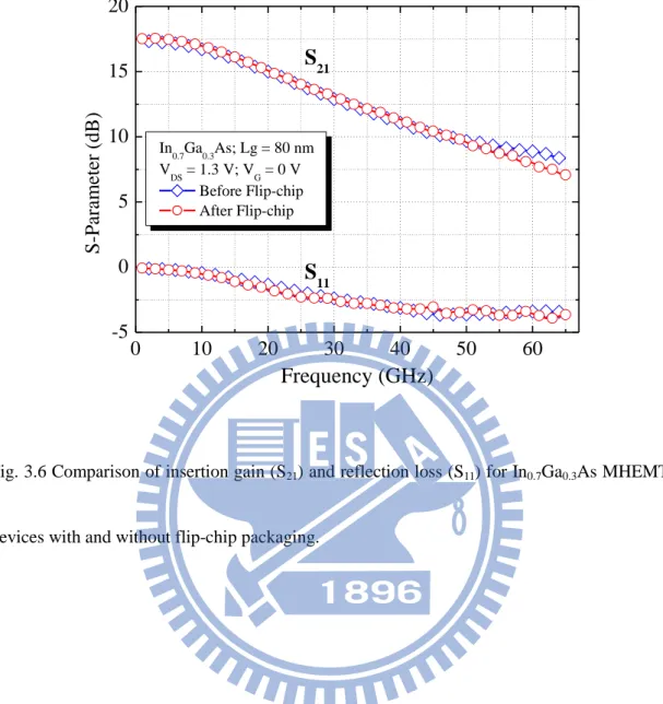
on the backside of the substrate. As observed from Fig. 3.6, the packaged device showed a high insertion gain of 7.5 dB at 60 GHz. The return loss (S11) and gain (S21)
remained the same for the bare device and packaged device at frequencies up to 50 GHz. However, the S21 of the flip-chip device showed a slight degradation for
frequencies above 50 GHz, which is attributed to the additional inductance induced from the bump transition. Besides, due to the good electrical conductivity of Au metal and the good interface transition achieved between the CPW Au plated circuit and Au bumps, the transmission losses on the signal transmission path was reduced.
35
To evaluate the feasibility of this packaged structure for MMWs low-noise applications, the noise figure (NF) of the In0.7Ga0.3As MHEMT device was
characterized with the frequency range of 22 to 60 GHz. The measured noise figures of the device before flip-chip assembly with different dc power consumptions at 54 GHz are shown in Fig. 3.7. As can be seen, the minimum noise figure (NFmin) was less 2 dB
below 10 mW power consumption. Fig. 3.8 shows the NFmin and the corresponding
associated gain (Ga) for the device with and without flip-chip package under the optimal bias conditions. The measured NFmin was 2.7 dB up to 60 GHz after flip-chip
packaging with 11 dB corresponding Ga. Meanwhile, for the device without package, the NFmin and Ga were 2.4 dB and 11.5 dB, respectively. Evidencing from the
measurement results, the DC and RF performances of the In0.7Ga0.3As MHEMT still
exhibited very good electrical performances up to 60 GHz after flip-chip package.
3.4 V-Band Flip-Chip Assembled Gain Block Using In
0.6Ga
0.4As
MHEMTs Technology
To demonstrate the applicability of the device for V-Band application, a two-stage gain block was designed and realized using the MIC approach. The adopted substrate was 127-μm-thick Al2O3 with a relative dielectric constant of 9.8. Microstrip
line circuits were patterned with 3μm thick Au metal. It is worth mentioned that the passive components, such as metal–insulator–metal (MIM) capacitors and thin-film resistors (TFRs), are excluded in the circuit realization to ensure that the fabrication process is simple and straightforward along with the flip-chip packaging. The main
36
advantage of this approach lies in the fact that the inclusion of matching circuits on the original carrier for flip-chip packaging provides a cost-effective solution for seamless integration of the device into the circuit.
Fig. 3.9 shows the circuit diagram of the two-stage gain block designed at 60 GHz. The matching circuits with the included bumps at the input, output, and interstage were designed for conjugate matching of the S-parameters and were realized with transmission lines and open stubs. Bandpass filters with coupled-line configuration were employed for DC blocking in the input, output, and interstage circuits. The gate and drain bias were supplied through the biasing network consisting of high impedance lines and radial stubs. The geometries of the radial stubs were determined through electromagnetic simulations so that the impedance levels were high enough to prevent the RF signal from leaking to the DC path. Fig. 3.10 shows the measured S-parameters of the fabricated gain block. Both stages were biased at VDS = 0.5 V and VGS = 0.4 V, corresponding to a total DC power consumption of 20
mW. A measured small-signal gain of 9 dB was obtained at 60 GHz with effective input and output S11. The loss in gain performance was mainly from the insertion loss
of the bandpass filters at the input and output ends. The metallic loss of the input, interstage, and output matching networks also contributed to the overall loss. The favorable agreement between the simulated and measured performances validated the design method.
37
3.5 Summary
The in-house fabrication of the flip-chip package of 80-nm gate In0.7Ga0.3As
MHEMT device on Al2O3 substrate was presented. After flip-chip packaging, the
device showed high IDS = 435 mA/mm at VDS= 1.5 V, and high gm= 930 mS/mm at
VDS= 1.5 V, which is almost the same as the bare chip performance. The packaged
devices also showed very small change in RFcharacteristics with NFmin of 2.7 dB and
Ga of 11 dB at 60 GHz after packaging.The flip-chip packaged low noise In0.7Ga0.3As
MHEMT device exhibited superior DC and RF performance, demonstrating the feasibility of using the proposed flip-chip technology for MMWs low noise applications.
To demonstrate the applicability of device using MICs design for V-band applications, a two-stage gain block at 60 GHz was designed and realized using a simple fabrication process. A 150 nm gate In0.6Ga0.4As mHEMT device was flip-chip
packaged on an Al2O3 substrate. The small signal gain was measured to be 9 dB at 60
GHz with only 20 mW DC power consumption. The superior performance proved the applicability of such technology as a cost-effective solution for 60 GHz applications.
38
Fig. 3.1 Epitaxial layer structure of the In0.7Ga0.3As high electron mobility transistors
39
Fig. 3.2 (a) Image of the in-house fabricated 80-nm gate In0.7Ga0.3As MHEMT device,
(b) The SEM image of the electroplated micro Au bumps (c) The schematic of the
flip-chip packaged structure (d) Image of the flip-chip packaged In0.7Ga0.3As
MHEMT device on Al2O3 substrate.
(a)
(b)
(c)
40
Fig. 3.3 In-house fabrication flow of the alumina (Al2O3) substrate for flip-chip packaging
41 0.0 0.3 0.6 0.9 1.2 1.5 0 100 200 300 400 500 D rai n C urrent I DS (m A /mm ) Drain-source Voltage VDS (V) In 0.7Ga0.3As HEMTs Lg = 80 nm; V G -0.6 ~ 0.2 V Before Flip-chip After Flip-chip
Fig. 3.4 Comparison of drain-source current (IDS) versus drain-source voltage (VDS) curves
with various gate voltages (VG) of In0.7Ga0.3As MHEMT devices with and without flip-chip
42 -0.6 -0.4 -0.2 0.0 0.2 0 100 200 300 400 500 In 0.7Ga0.3As HEMTs Lg = 80 nm; V DS = 1.3 V Before Flip-chip After Flip-chip Gate-Source Voltage, V GS (V) D rai n current I DS (m A /m m ) 0 200 400 600 800 1000 Transconduct ance
g
m (m S/ m m )Fig. 3.5 Comparison of drain current density (IDS) and transconductance (gm) as a function of
gate-source voltage (VGS) at VDS = 1.3V for In0.7Ga0.3As MHEMT devices with and without
43 0 10 20 30 40 50 60 -5 0 5 10 15 20
S
11S
21 S -P ara m eter (d B) Frequency (GHz) In 0.7Ga0.3As; Lg = 80 nm VDS = 1.3 V; VG = 0 V Before Flip-chip After Flip-chipFig. 3.6 Comparison of insertion gain (S21) and reflection loss (S11) for In0.7Ga0.3As MHEMT
44 1 10 0 1 2 3 4 5 6 40 30 20 In 0.7Ga0.3As; Lg = 80 nm V DS= 1.0 V Frequency = 54 GHz N o ise Figu re (d B ) DC Power Consumption (mW)
Fig. 3.7 The minimum noise figure with different DC Power consumptions at VDS = 1 V for
45 0 1 2 3 4 5 6 7 8 9 60 50 40 30 20 In 0.7Ga0.3As; Lg = 80 nm V DS= 1.0 V; VGS= - 0.1 V Before Flip-chip After Flip-chip Frequency (GHz) N o ise Figu re (d B ) 0 2 4 6 8 10 12 14 16 18 A sso ci at ed G ai n (d B )
Fig. 3.8 Comparison of the minimum noise figure and associated gain at VDS = 1.0 V, VG =
46
Fig. 3.9 Circuit diagram of the two-stage gain block designed at 60 GHz.
Fig. 3.10 Measured S-parameters of the fabricated gain block biased at VDS = 0.5 V and VGS =
47
Chapter 4
Investigation of the Flip-chip Package with BCB Underfill for
W-band Applications
Flip-chip package is promising for MMWs applications. However, the CTE mismatch between the chip and the substrate generates thermal stresses that fracture the flip-chip structure. The use of underfills with low dielectric loss is essential to improve the mechanical strength and reliability of the flip-chip package. BCB (Benzocyclobutene) was used in this study as the underfill material for the flip-chip structure using the no-flow process. The flip-chip structure with BCB injection provides good RF performance with a S11 of better than 18 dB and an S21 of 0.6 dB up
to 100 GHz. Furthermore, thermal cycle and shear force tests showed that the underfill injection can significantly improve the reliability of a flip-chip package.
4.1 Background and Motivations
Wireless communication and imaging systems at MMW and sub-MMW frequencies are gaining increasing attention. Packages with good electrical performance, decent mechanical reliability and low cost are crucial for high frequency applications. Flip-chip interconnects are considered as a promising interconnect technology due to several reasons [31,55]. Compared with conventional wire-bonding technology, flip-chip has much shorter interconnects, significantly reducing the parasitic effects at MMW frequencies [56]. However, the reliability of flip-chip
48
packaging is critical due to the thermal mechanical stresses from CTE mismatch of substrate and chip CTE [38,57]. Many previous studies have investigated the underfill effect in a flip-chip structure [23,40,48]. Kusamitsu et al. demonstrated LNA flip-chip bonded Al2O3 with an epoxy-based underfill with response shifted in frequency due to
the underfill injection [23]. Feng et al. presented increase in the fatigue life with only a small additional loss of flip-chip assemblies [38]. Improvement in the reliability with small loss of flip-chip structure on polymer substrate has also been achieved in [49].
Conventional epoxy-based underfill has a high dielectric loss tangent which induces extra signal dissipation and degrades RF performance. Previously, by performing the EM simulations, we demonstrated that the loss can be further reduced using lower loss underfill materials [40]. Therefore, the important considerations of underfill materials are low loss tangent, good thermo-mechanical properties and good process compatibility. BCB is a good candidate as an underfill material. Table 4.1 summaries the material properties of conventional epoxy resin and BCB. BCB is designed for high frequency and low-k applications. It has been used for device passivation, interlayer dielectrics, and stress buffer layer. In general, BCB has a lower loss tangent than epoxy resin, making it very promising for MMW applications. The moisture uptake is also an important concern because moisture inside the materials can increase the dielectric loss at high frequencies [58, 59, 70].
49
4.2 Fabrication and Flip-chip Package Process
In-house flip-chip interconnect structure with BCB underfill was performed in this study. The fabrication processes of the GaAs thru-line chip and alumina (Al2O3)
substrate have been described in Chapter 2. Figure 4.1 (a) shows a schematic of the flip-chip structure. The total signal transmission path was 3 mm, including CPW on the Al2O3 substrate, CPW on the GaAs chip, and two flip-chip transitions. An
optimized no-flow underfill process, which will be described as follows, was applied to fill BCB into the flip-chip structures. The characteristic impedance (Z0) of the
CPW transmission line on the GaAs chip and the Al2O3 substrate was designed to be
50 Ω. The underfill (r>1) injection changes the effective dielectric constant and
results in an impedance mismatch which degrades the chip performance. To reduce the impact of the underfill, the CPW transmission line on GaAs was designed to achieve an impendence matching of 50 Ω. Compensation designs, such as ground pad shrinking and high impendence line, were also adopted on the substrate transmission line to compensate for the parasitic capacitance of the flip-chip interconnects as shown by Fig. 4.2. After implementing matching designs, the RF performance was evaluated and is presented in the next section.
Conventionally, a capillary underfill process is used to inject epoxy resin into the flip-chip structure. Unfortunately, liquid BCB cannot easily flow into the gap between the chip and substrate using capillary force. To solve this issue, the no-flow underfill process was proposed as shown in Fig. 4.3. Liquid BCB was first deposited on the substrate. Then the substrate was heated to cause BCB to flow. The heating conditions, such as the heating time and temperature, were optimized to enhance the BCB flow.
50
Finally, the chip and the substrate were flip-chip bonded by using the Au-to-Au thermo-compression method. An additional curing at 250 oC for 2 hours was performed to facilitate cross-linking of the BCB polymer chains. Figure 4.1 (b) shows a cross-sectional SEM image of the flip-chip structure with BCB underfill. The BCB was successfully injected into the flip-chip interconnect structure using the no-flow underfill process.
4.3 Measured Results of the Flip-chip Packaging Structure with
Underfill Injection
The losses in the flip-chip interconnects with underfill include mismatch loss and real loss. Mismatch loss is mainly due to the dielectric constant change from the underfill. To reduce the impact from the underfill, the dimensions of the chip transmission line were modified, and compensation designs on the substrate transmission line were adopted. Figure 4.4 shows comparison of the flip-chip interconnects with and without underfill. The flip-chip with BCB has lower loss than the flip-chip with epoxy at high frequencies. The S11 and S21 of the flip-chip structure
with BCB were better than 18 dB and 0.6 dB, respectively, from DC to 100 GHz. As for the case of flip-chip sample without underfill, an S21 of 0.66 dB was observed.
The corresponding contribution to the overall S21 at 90 GHz were further extracted to
be 0.14 dB from the CPW trace on GaAs substrate, 0.26 dB from CPW on Al2O3, and
0.26 dB from the transition. It was then concluded that the optimized design can effectively reduce the mismatch loss.
51
radiation loss can be neglected because it is very small. The dielectric loss is composed of chip loss (LC), substrate loss (LS) and underfill loss (LUF). After the
underfill injection, the extra dielectric loss induces and degrades the transmission properties. Hence, to investigate the influence of underfill injection, the loss factor is calculated using (1) [60]:
2 2
Loss Factor = 1S11 S21 (1)
The underfill loss can be calculated by subtracting the loss of the flip-chip without underfill from the loss of flip-chip with underfill. The losses of chip, substrate, and metal in the flip-chip structure are also extracted by electromagnetic simulation for comparison. Figure 4.5 shows the comparison of the loss factors between the metal, chip, substrate, epoxy, and BCB. As can be seen, the major losses are metal loss and underfill loss. The epoxy loss is near the metal loss. The BCB loss is lower than epoxy loss. The flip-chip package with BCB shows a lower insertion loss of 0.11 dB/mm compared to the epoxy loss of 0.24 dB/mm at 100 GHz. These results demonstrate that underfill materials with lower dielectric loss tangents, such as BCB, can effectively reduce the RF loss of the flip-chip assembly caused by the underfill. Given that fact that the metal loss contributed the most to the total loss as shown in Fig. 4.5, it is worth mentioning that for Si Complementary Metal–oxide– semiconductor (CMOS) process where much narrower traces are encountered, the improvement in overall loss due to BCB might not be as pronounced since the metal loss are much higher for such cases.