P122 ECS Journal of Solid State Science and Technology, 3 (5) P122-P125 (2014) 2162-8769/2014/3(5)/P122/4/$31.00©The Electrochemical Society
Characterization of Ultra-Thin Ni Silicide Film by Two-Step Low
Temperature Microwave Anneal
Chien-Ting Wu,a,zYao-Jen Lee,a,bFu-Kuo Hsueh,a,cPo-Jung Sung,a,cTa-Chun Cho,c
Michael Ira Current,dand Tien-Sheng Chaoc
aNational Nano Device Laboratories, National Applied Research Laboratories, Hsinchu City, Taiwan bDepartment of Physics, National Chung Hsing University, Taichung, Taiwan
cDepartment of Electrophysics, National Chiao Tung University, Hsinchu, Taiwan dCurrent Scientific, San Jose, California 95124, USA
A novel silicide process with two-step low temperature microwave annealing (MWA) achieves NiSi thickness of 10 nm while maintaining low resistance, and an ultra-thin Ni silicide film, only 4.5 nm, has been realized. In this MWA system, we insert quartz and Si susceptors to change the absorption efficiency of the process wafer and provide fine turning in temperature control during annealing. The thickness of NiSi film is determined by microwave power and by changing the number and the position of quartz and Si susceptors in the first step of the anneal process. The STEM-HAADF combined EELS/EDS spectroscopies are used to analyze the electronic excitations and identify the phase of Ni silicide.
© 2014 The Electrochemical Society. [DOI:10.1149/2.006405jss] All rights reserved.
Manuscript submitted January 20, 2014; revised manuscript received February 20, 2014. Published March 6, 2014.
NiSi, a transition metal silicide, has been increasingly used for con-tacts in the latest complementary metal oxide semiconductor (CMOS) devices, owing to its low temperature of formation and low Si con-sumption during silicidation, low sheet resistance (RS) and lower leakage current.1,2The use of NiSi currently faces a difficult trade-off
between thickness and sheet resistance. The contact junction depth must still scale with gate length. To avoid high contact resistance and high contact leakage, no more than half the contact junction depth can be consumed in the formation of the silicide. Therefore, the silicide must become progressively thinner to accommodate the more shal-low contact junction for scaled contacts. The rapid thermal annealing (RTA) has been widely used for silicidation and exhibits difficult thin-thickness and phase control. Microwave annealing (MWA)3has been
realized to activate implanted dopants through solid phase epitaxial regrowth at low temperature.4It is promising for achieving advanced
Si or Ge CMOS because of its unique volumetric heating and low temperature due to apparent non-thermal energy transfer.5 The
ad-vantages of replacing rapid thermal annealing (RTA) with MWA are ultra-thin NiSi formation, diffusion-less junction, improved capacity of gate oxide and lower gate leakage. In this work, a novel two-step low temperature MWA process is used to form homogeneous NiSi contact films with low sheet resistance while not sacrificing thickness and quality.
During silicidation, many kinds of nickel silicide phases may ap-pear simultaneously.6It has been reported that the predominant phases
are Ni2Si, NiSi and NiSi2, form in the ranges 200–350, 350–750, and 750–1000◦C, respectively.7The NiSi has the lowest resistivity among
three different phases and other metal silicides. Furthermore, the Ni atoms are the primary moving species during the formation of NiSi phase. It could prevent the bridging effect which results in short cir-cuit area between gate and source/drain.8 It is well recognized that
identification of nickel silicide phases after annealing is of crucial im-portance to its performance, especially, while these phases are formed in nano-polycrystalline layer. In this study, we use electron energy-loss spectroscopy9–13and energy dispersive X-ray spectroscopy13,14in
con-junction with scanning transmission electron microscopy14
(STEM-EELS/EDS) in order to identify the nickel silicide phases concen-trating primarily on the Z-contrast image with atomic spatial resolu-tion, elemental analysis, bulk plasmon excitaions and the chemical bonding.
Experimental
Two-step low temperature MWA.— Low resistance and ultra-thin
NiSi is achieved by inserting quartz and Si susceptors above and
be-zE-mail:[email protected]
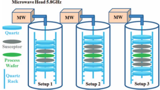
low the process wafer during MWA. Figure1shows the schematic illustration of the MWA system. Si susceptors placed near the process wafer improve the uniformity of microwave energy absorption. The absorption of microwave power by quartz wafers is negligible. How-ever, quartz wafers will absorb the heat from Si susceptors and help system to heat evenly. Therefore, quartz and Si susceptors change the absorption efficiency of the process wafer and provide fine turning in temperature control during MWA.
According to our experiments, the 10 nm Ni film shows better uniformity control of NiSi films than 5 nm Ni film. Moreover, when the thickness of Ni film decreases to 3 nm, it is easy to form a local NiSi2phase with a pyramidal structure penetrating into the underlying Si. A nominal 10 nm Ni film was pre-deposited on Si wafer by physical vapor deposition (PVD) with bias contact at the back side. Two-step annealing for NiSi layer formation was carried out by MWA processes. MWA uses a 5.8 GHz microwave source that results in heating of the bulk Si and Ni films. Each annealing step lasted for 300 sec.
A thin nickel silicide layer with partial crystallinity was formed by first MWA step. Then, we removed unreacted metal (Ni rich layer, Ni:>93%) by selective wet etching with H2SO4:H2O2(3:1) solution at 120◦C. After removing excess Ni, the second step MWA was per-formed. The thermal budget of the second step MWA is sufficient to transform the original partial-crystalline silicide into crystalline NiSi films with slightly increasing the silicide thickness.
STEM-EDS/EELS measurements.— In addition, our EELS/EDS
work was carried out in a FEI (Tecnai F20; 200 kV) STEM capa-ble of forming an electron probe as small as 0.2 nm and an energy
Figure 1. (Color online) Schematic illustration of the MWA system. Quartz and Si susceptors inside the chamber change the absorption efficiency of the process wafer.
) unless CC License in place (see abstract).
ecsdl.org/site/terms_use
address. Redistribution subject to ECS terms of use (see
140.113.38.11
ECS Journal of Solid State Science and Technology, 3 (5) P122-P125 (2014) P123
Table I. The summarized conditions of silicidation. All samples (A,B and C) use 10 nm Ni film and vary in power levels, one or two step MWA, and setup 1 versus setup 2.
First-Step MWA Second-Step MWA
Sample Setup 1 Setup 2 Setup 3 NiSi Thickness
A 600 W 240◦C – 1200 W 360◦C 16 nm
B – 600 W 196◦C 1200 W 360◦C 10 nm
C 540 W 233◦C – 1200 W 360◦C 4.5 nm
resolution of∼0.6 eV. With the 0.2 nm electron probe, we can ex-plore the electronic excitation of an individual nano-object with high spatial resolution. The high-angle annular dark-field (HAADF) image with atomic spatial resolution (∼1 angstrom) was carried out in an aberration-corrected STEM (JEOL JEM 2100F).
Results and Discussion
A series of NiSi films (samples A,B and C) using MWA are per-formed and summarized in TableI. We supply different thermal bud-gets and setups in first-step MWA leads to various silicide thickness. All samples used the same optimum condition in setup 3 chamber with 1200 W microwave power in the second step annealing. 16 nm (sam-ple A) and 10 nm (sam(sam-ple B) NiSi film are achieved by using setup 1 and setup 2 chambers, respectively, with 600 W microwave power in the first step MWA and followed by second-step MWA. The setup 1 chamber totally uses two Si susceptors and four quartz wafers above and below the process wafer. The setup 2 chamber added one more Si susceptor above the process wafer in order to absorb microwave energy and then reduce the process temperature. The maximum wafer surface temperatures in setup 1 and setup 2 chambers are 240◦C and 196◦C, respectively, as measured with a thermal label. The setup 3 chamber totally uses four Si susceptors and four quartz wafers above and below the process wafer with 1200 W microwave power. The maximum temperature on process wafer surface rises above 360◦C as measured with an infrared thermometer from back-side (a thermal label showed a maximum temperature of about 300◦C). Here, we note that the measured temperature should be considered as approximate due to the difficulties of temperature measurement in a microwave process chamber.
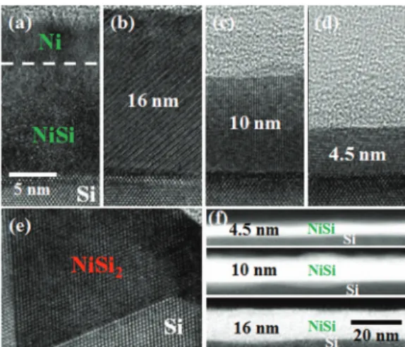
When MWA at 600 W was used with more than three Si suceptors, the resutling NiSi had poor thickness uniformity and mixed phases. A 4.5 nm NiSi film with very few NiSi2 nano-islands, sample C, could be achieved by using setup 1 chamber with lower microwave power, 540 W, for the first step MWA. The maximum temperature on the process wafer surface is 233◦C. Figures2a∼ 2eshow the [1–10]Si substratecross-sectional HRTEM images of thin silicide layers. Figure2ashows a typical thin silicide layer with partial crystalline and unreacted Ni (on top) was formed by the first step MWA of sample B. After the second step MWA, silicide thickness is slightly increased from 9 nm to 10 nm. Figures2b∼2dshow the HRTEM images of NiSi thin film samples A (16 nm), B (10 nm) and C (4.5 nm) after two-step MWA processes. In the HRTEM images, the large grain crystalline NiSi phase, without NiSi2penetration into Si could be observed and identified by its d-spacing.15
In our previous studies, a series of samples comparing two-step RTA/RTA, RTA/MWA and MWA/RTA anneals was carried out. Ac-cording to these experiences, it is easy to form NiSi2 phase with pyramidal structure penetrating into the underlying Si, as shown in Fig. 2e, after RTA or MWA process with higher thermal budget. Furthermore, while the thickness of nickel silicide reduces, a mixed NiSi/NiSi2phase is easy to form even for temperatures below 750◦C. Low-temperature MWA process and the formation of a partially crys-talline NiSi layer in the first step are the key to achieve the ultra-thin NiSi film without penetrating NiSi2 phases. Furthermore, the thick-ness of NiSi film is determined by microwave power and by changing the number and the position of quartz and Si susceptors in the first step
Figure 2. (Color online) HRTEM images and HAADF images of NiSi thin films. (a) A typical thin silicide layer with partial crystalline was formed by first step MWA of sample B. (b∼ d) 16 nm, 10 nm and 4.5 nm NiSi thin films after two-step MWA. (e) A typical NiSi2phase with pyramids structure penetrating into the underlying Si after RTA or MWA process at higher temperature. (f) HAADF images of NiSi thin films with different thickness.
of the anneal process. Moreover, the uniformity of NiSi film could be improved by chamber design, such as wafer rotation during process with quartz susceptor-assisted.16
As the silicide thickness is pushed to below 10 nm after RTA or MWA process, in experience, it is easy to form nano structures with NiSi2 phases in the silicide layer.17–19Figure3shows the [1– 10]Si substratehigh-resolution HAADF image of the 4.5 nm NiSi sample, with the brightest contrast signifying NiSi (green inset, Fig.3) and the bright one in the right inset directing to NiSi2(red inset, Fig.3) taking into account the weight sensitivity of the STEM-HAADF technique. It clearly shows a 4.5 nm NiSi thin film formed with a few, small and non-penetrating epi-NiSi2 (10∼ 20 nm) regions at Si surface. These small NiSi2regions are not observed in 10 nm and 16 nm NiSi films. The volume fraction of NiSi2nano-island in 4.5 nm NiSi thin film is below 10%. By the HAADF imaging, lattice parameters of Si and NiSi2 are similar (Si: 0.5430 nm, NiSi2: 0.5406 nm),13 and the
in-plane mismatch between the atomic spacing on the NiSi2 (111) and Si (111) planes is only 0.5%. Therefore a NiSi2 layer is easy to form by epitaxial growth on Si(111) oriented substrates, as shown in right-insert figure in Fig.3with an epitaxial relation of NiSi2(111) // Si (111).20
In addition, the STEM combined EELS/EDS spectroscopies were also performed to identify the phase of nickel silicide. The Si ele-mental compositions of NiSi and NiSi2in Fig.3by STEM-EDS are
Figure 3. (Color online) The [110] cross-sectional HAADF image of 4.5 nm NiSi sample. In this imaging mode, the intensity of scattering scales with the atomic number Z as Z1.7, so the brightest features are NiSi (left insert), the gray-white features are epi-NiSi2(right insert), and the Si substrates are weakly visible.
) unless CC License in place (see abstract).
ecsdl.org/site/terms_use
address. Redistribution subject to ECS terms of use (see
140.113.38.11
P124 ECS Journal of Solid State Science and Technology, 3 (5) P122-P125 (2014)
Figure 4. (Color online) (a) EELS low-loss spetra of Si, NiSi2 and NiSi. (b) A typical XPS Ni-L2,3edge spectrum of NiSi film. And the ELNES Ni-L2,3edge spectra of NiSi2and NiSi films.
∼52% and ∼69%, respectively. Moreover, the Si elemental composi-tions in 10 nm and 16 nm NiSi films are 50% approximately. Fig.4a shows portion of the STEM-EELS spectra taken across the interface with the electron probe pinpointing the observed Si, NiSi and NiSi2, respectively. Upon positioning the electron probe at Si (Fig.4a), we observed the characteristic bulk-plasmon excitation, 16.7 eV,21,22of
the material. The readily observed bulk-plasmon excitations of NiSi2 (19.7 eV) and NiSi (20.3 eV) in Fig.4aare also nicely consistent with the known values of the respective materials,10in agreement with the
STEM-EELS characterizations in Fig.3. Furthermore, the variation of the binding energy of the Ni L2,3edge between pure nickel and nickel silicides are known to be 0.1∼ 1.9 eV (from Ni to Ni3Si, Ni31Si12, Ni2Si, NiSi, NiSi2).23,24The chemical shifts of the Ni L2,3edge
be-tween NiSi and NiSi2 is only 0.7 eV. However, there is no standard material, such as pure nickel, to be used as a reference for energy calibration in the sample. Therefore, the chemical shifts of core loss peaks are difficult to identify as NiSi and NiSi2phases. The branching (spin-orbit splitting) ratio of the L2,3edge is a candidate to be consid-ered based on the information about oxidation state.25A typical X-ray
photoelectron spectroscopy (XPS) spectrum of NiSi film is shown as an open-square (blue color) curve in Fig.4b. The branching ratio can be calculated from the transition probability of 2p1/2 and 2p3/2 elec-trons to 3d orbits with background subtraction, and the ratio is 0.74 in agreement with the result of 0.75∼ 0.77 in previous studies.11,26,27
In this study, the NiSi2phase is formed in small grain sizes in nano-scale which is difficult to obtain through XPS measurements due to its limited spatial resolution (∼15 μm). The spatially-resolved technique of STEM-EELS becomes an otherwise approach for study-ing the Ni-L2,3edge ELNES of such nano-scale phase, as shown in Fig.4b. The dash-square (green color) and triangular-line (red color) curves in Fig.4bare the Ni-L2,3 edge ELNES spectra of NiSi and NiSi2, respectively, after background subtraction and Fourier-ratio de-convolution of the plural scattering effects. The intensities had been
Figure 5. (Color online) (a) The variation of sheet resistance of NiSi thin film after one or two step MWA process using 10 nm Ni thin film. (b) The thermal stability of NiSi thin films of A (16 nm), B (10 nm) and C (4.5 nm) samples.
normalized to the L2maximum peak of each phase. It is clear that L3 peak becomes smaller relative to the L2peak if the Si concentration in-creases. The branching ratio, which is defined as I(L3)/[I(L2)+I(L3)], of NiSi and NiSi2are 0.73 and 0.70, respectively, in agreement with the result of Asayama’s work (NiSi: 0.74, NiSi2: 0.68).26
After the first MWA step, the silicide thickness is extremely thin and the RS is relatively high, as shown in Fig. 5a. After we ap-ply a second MWA step, the RS is markedly improved. The RS of 16 nm, 10 nm and 4.5 nm NiSi films were reduced to 11, 18 and 50 ohm/sq. from 130, 170 and 240 ohm/sq., respectively. As ex-pected, the thicker NiSi film has a lower RSvalue. Furthermore, the higher sheet resistance of 4.5 nm-thick NiSi film should be attributed to more scattering for thinner film. Fig.5bshows good thermal stabil-ity of NiSi films at least 450◦C (4.5 nm NiSi) and 600◦C (10 nm and 16 nm NiSi).
Conclusions
In conclusion, we demonstrate a novel silicidation process that forms NiSi thin films at a thickness of 10 nm while maintaining a low Rs. with two-step low temperature MWA. Using this method, an ultra-thin Ni silicide film, as thin as 4.5 nm, can be fabricated. The thickness of NiSi film is determined by microwave power and by changing the number and the position of quartz and Si susceptors in the first step of the anneal process. The STEM-HAADF combined with EELS/EDS spectroscopies are also performed to identify the phase of nickel silicide.
Acknowledgments
Helpful discussions with Professor C. H. Chen, Professor M. W. Chu, Dr. S. C. Liou and Dr. C.-P Chang for STEM-EELS are acknowl-edged. This work was supported by the National Science Council under the project of NSC grant Nos. 101- -2112-M-492-002-MY3.
) unless CC License in place (see abstract).
ecsdl.org/site/terms_use
address. Redistribution subject to ECS terms of use (see
140.113.38.11
ECS Journal of Solid State Science and Technology, 3 (5) P122-P125 (2014) P125
References
1. T. Morimoto, T. Ohguro, S. Momose, T. Iinuma, I. Kunishima, K. Suguro, I. Katakabe, H. Nakajima, M. Tsuchiaki, M. Ono, Y. Katsumata, and H. Iwai,Electron Devices, IEEE Transactions on, 42, 915 (1995).
2. J. A. Kittl, A. Lauwers, O. Chamirian, M. Van Dal, A. Akheyar, M. De Potter, R. Lindsay, and K. Maex,Microelectron. Eng., 70, 158 (2003).
3. Y.-J. Lee, L. Yu-Lun, H. Fu-Kuo, H. Kuo-Chin, W. Chia-Chen, C. Tz-Yen, H. Ming-Hung, J. M. Kowalski, J. E. Kowalski, H. Dawei, C. Hsi-Ta, L. Yiming, C. Tien-Sheng, W. Ching-Yi, and Y. Fu-Liang, presented at the IEEE International Electron Devices Meeting (2009).
4. L. Yu-Lun, H. Fu-Kuo, H. Kuo-Ching, C. Tz-Yen, J. M. Kowalski, J. E. Kowalski, Y.-J. Lee, C. Tien-Sheng, and W. Ching-Yi,Electron Dev. Lett., IEEE, 31, 437 (2010). 5. J. H. Booske, R. F. Cooper, and I. Dobson,J. Mater. Res., 7, 495 (1992). 6. B. Cafra, A. Alberti, L. Ottaviano, C. Bongiorno, G. Mannino, T. Kammler, and
T. Feudel,Mater. Sci. Eng.: B, 114–115, 228 (2004).
7. M. Tinani, A. Mueller, Y. Gao, E. A. Irene, Y. Z. Hu, and S. P. Tay,J. Vac. Sci. Technol. B:19, 376 (2001).
8. H. Iwai, T. Ohguro, and S. Ohmi,Microelectron. Eng., 60, 157 (2002). 9. M. C. Cheynet and R. Pantel,Micron, 37, 377 (2006).
10. T. H. Shohei Terada, Naoto Hashikawa, and Kyoichiro Asayama,Jpn. J. Appl. Phys., 48, 011203 (2009).
11. E. Verleysen, H. Bender, O. Richard, D. Schryvers, and W. Vandervorst,J. Microsc., 240, 75 (2010).
12. N. Kawasaki, N. Sugiyama, Y. Otsuka, H. Hashimoto, H. Kurata, and S. Isoda,J. Appl. Phys., 109, 063716 (2011).
13. N. Kawasaki, N. Sugiyama, Y. Otsuka, H. Hashimoto, M. Tsujimoto, H. Kurata, and S. Isoda,Ultramicroscopy, 108, 399 (2008).
14. E. Verleysen, H. Bender, O. Richard, D. Schryvers, and W. Vandervorst,J. Mater. Sci., 46, 2001 (2011).
15. F. d’Heurle, C. S. Petersson, J. E. E. Baglin, S. J. L. Placa, and C. Y. Wong,J. Appl. Phys., 55, 4208 (1984).
16. Y.-J. Lee, H. Fu-Kuo, M. I. Current, W. Ching-Yi, and C. Tien-Sheng,Electron Dev. Lett., IEEE, 33, 248 (2012).
17. J. Luo, Z. Qiu, C. Zha, Z. Zhang, D. Wu, J. Lu, J. Åkerman, M. ¨Ostling, L. Hultman, and S.-L. Zhang,Appl. Phys. Lett., 96, 031911 (2010).
18. Z. Zhang, S.-L. Zhang, B. Yang, Y. Zhu, S. M. Rossnagel, S. Gaudet, A. J. Kellock, J. Jordan-Sweet, and C. Lavoie,Appl. Phys. Lett., 96, 071915 (2010).
19. K. De Keyser, C. Van Bockstael, R. L. Van Meirhaeghe, C. Detavernier, E. Verleysen, H. Bender, W. Vandervorst, J. Jordan-Sweet, and C. Lavoie,Appl. Phys. Lett., 96, 173503 (2010).
20. U. Falke, A. Bleloch, M. Falke, and S. Teichert,Phys. Rev. Lett., 92, 116103 (2004).
21. C. H. Chen, J. Silcox, and R. Vincent,Phys. Rev. B, 12, 64 (1975).
22. C.-T. Wu, M.-W. Chu, S.-B. Wang, M.-S. Hu, K.-H. Chen, L.-C. Chen, C.-W. Chen, and C. H. Chen,Appl. Phys. Lett., 96, 263106 (2010).
23. Y. Cao, L. Nyborg, and U. Jelvestam,Surf. Interface Anal., 41, 471 (2009). 24. P. L. Tam, Y. Cao, U. Jelvestam, and L. Nyborg,Surf. Coat. Technol., 206, 1160
(2011).
25. R. F. Egerton, Electron Energy-Loss Spectroscopy in the Electron Microscope, Plenum Press, New York (1996).
26. K. Asayama, N. Hashikawa, M. Kawakami, and H. Mori, in Microscopy of Semi-conducting Materials 2007, A. G. Cullis and P. A. Midgley, Editor, Vol. 120, pp. 329-332, Springer Netherlands (2008).
27. E. Verleysen, H. Bender, D. Schryvers, and W. Vandervorst,J. Phys.: Conf. Ser., 209, 012057 (2010).
) unless CC License in place (see abstract).
ecsdl.org/site/terms_use
address. Redistribution subject to ECS terms of use (see
140.113.38.11