The Random Telegraph Noise (RTN) Analysis
in Ultra Thin High-
κκκκ
Metal Gate CMOS Device
i
CMOS
Random Telegraph Noise(RTN)
RTN
(ET0)
ii
Abstract
As the scaling of the CMOS technology advances aggressively, the Random Telegraph Noise (RTN) becomes an important reliability issue.[1] Since RTN is a stochastic fluctuation between two levels of either the device drain current (ID) or
threshold voltage (Vt) induced by trapping/de-trapping of a single charge in a gate
trap.
In this work, we demonstrate a method to extract RTN trap position both in vertical direction (channel surface to gate electrode) and lateral direction (source to drain). Therefore, the traps in gate dielectric can be profiled.
Finally, we extract RTN trap energy at zero electric field condition (ET0) in
iii
iv
Contents
Chinese Abstract
iEnglish Abstract
iiAcknowledgement
iiiContents
ivFigure Captions
vChapter 1
Introduction
1Chapter 2
Trap Position Extraction
72.1 Introduction 7
2.2 RTN Trap Lateral Position Extraction 7 2.3 RTN Trap Vertical Position Extraction 8
Chapter 3
Measurement Data Analysis and Discussions
143.1 Introduction 14
3.2 Measurement Setup and Analysis Method 14 3.3 Percolation Effect 15
Chapter 4
Analysis of Trap Energy
254.1 Introduction 25
4.2 Cause of VG Dependent Difference 25
4.3 RTN Trap Energy in Flat Band Extraction 25
Chapter 5
Conclusions
37v
Figure Captions
Chapter 1
Fig.1.1 Illustration of a channel electron capture and emission by an interface trap
in our high-κ metal-gate MOSFET. And drain current waveform resulting from electron emission and capture at an interface trap.
Fig.1.2 RTN is observable when trap of energy level ET is a few kT different from
the Fermi level EF.
Fig.1.3 A typical drain current waveform of single level RTN induced current
fluctuation @(VG=0.45V VD=0.05V).
Fig.1.4 Drain current waveform of Multi-level RTN. RTN amplitudes are different
from the same device caused by percolation effect.
Chapter 2
Fig.2.1 Illustration of lateral position extraction of RTN trap. The voltage in
channel is proportion to lateral position.
Fig.2.2 Band diagram of a trap with a vertical position (XT) and a trap energy (ET)
in SiO2 layer.
Fig.2.3 Reference values of negative (a) and positive (b) slopes using 1D Poisson
equation simulation.
Table.1 is a trap vertical position extraction in different gate dielectric layers.
Chapter 3
Fig.3.1 Illustration of measurement setup and we use Agilent 4155 to measure the
high-κ and metal gate stack CMOS devices.
vi
VD1 and VD2. Second, obtain the time constant ratio <τc>/<τe> in different
VG with VD1. Third, plot ln(τc/τe) versus VG with VD1, obtain its slope and
compare with our reference points which indicates the trap locates in either HK or IL. Therefore, we can extract the trap vertical position from Table.1. Finally, repeat the steps before with VD2. Then obtain ∆VTS and the trap
lateral position can be extracted by Eq.2.1.
Fig.3.3 A two level RTN pattern with varies gate voltage, τc becomes smaller as
gate voltage VG increases. ΔVTS is the voltage difference at same time
constant ratio.
Fig.3.4 A two level RTN pattern with varies gate voltage. Capture time constant τc
becomes larger as gate voltage VG increases.
Fig.3.5 (a) is trap distribution along vertical direction. Most of traps locate in HfO2
layer. (b) is trap distribution along lateral direction, which exhibits an uniform distribution.
Fig.3.6 Illustration of channel surface potential and current pattern.
Fig.3.7 When interface trap charge position locates on the main current path, will
induce large drain current fluctuation ∆Id.
Fig.3.8 RTN amplitude distribution with different cell width. σ becomes large as
cell width is decrease.
Chapter 4
Fig.4.1 Definitions of two different types trap. We regard negative and positive VG
dependence as Type A trap and Type B trap.
Fig.4.2 Cause of VG dependent difference. Type A traps and Type B traps are
interact with channel and gate electrode respectively.
vii
condition ET0. The gate voltage varies from flat band voltage VFB to VG0.
When VG=VG0, the trap energy ET aligns to Fermi level EF.
Fig.4.4 Window on ET0 over XT plane where the trap locates within the window can
be characterized.
Fig.4.5 Shows the traps energy distribution in common case and our case. For our
devices, we consider surface potential variation rate.
Fig.4.6 Shows the number of traps in different EOT devices. Type B traps is
observable when EOT scaling down to 7.8Å.
Fig.4.7 Type B trap is observable due to |VFB| decreases. Therefore the defect band
overlap the triangle window, Type B trap can be characterized.
Fig.4.8 The average of RTN amplitude of Type B trap is nearly equal to that of Type
A. Type B trap will induce reliability problems in modern devices.
1
Chapter 1
Introduction
Metal-Oxide-Semiconductor-Field-Effect-Transistor (MOSFETs) has been widely utilized in the past few decades. When device geometry scale down to nanotechnology, the random telegraph noise (RTN) becomes an important reliability issue. It will reduce the device performance in both analog and digital circuit.[2] RTN has been proposed in recent years. Fig.1.1 is an illustration of our MOSFETs cell structure and typical Two level RTN pattern, where (i) <τc> means not only capture
time but average of empty trap state time, (ii) <τe> means either emission time or
average of empty trap state time, and (iii) ∆Id is the current fluctuation between two
levels. Fig.1.2 shows RTN is observable when trap of energy level ET is a few kT
differences to the Fermi level EF, where k is the Boltzmann’s constant, T is
equilibrium temperature. The trap of energy level can be extracted from RTN according to the following equation [3]:
Eq.1.1
where g is degeneracy factor, <τc> and <τe> are average of capture and emission
times, k is the Boltzmann’s constant and T is temperature. If we can obtain the time constant ratio <τc>/<τe>, the trap of energy ET can be extracted. Fig.1.3 shows a
typical single level RTN and obtains the time constant ratio <τc>/<τe>. Fig.1.4 shows example of multi-level RTN. However, the RTN amplitudes are different from the same device caused by percolation effect. The percolation effect will be introduced in the chapter 3. exp( ) exp( ) c T F T F e E E E E g kT kT τ τ < > = − ∝ − < >
2
There are five chapters in this thesis. Chapter 1 is a brief introduction to RTN and its most important three parameters <
τ
c>, <τ
e> and ∆Id. In Chapter 2, we willextract trap position both in lateral direction (source to drain) and vertical direction (channel surface to gate electrode). In Chapter 3, demonstrate the measurement process flow chart and its result discussions. The extraction of trap energy at zero electric field condition ET0 will be characterized in Chapter 4. Finally, we make
3
Fig.1.1 Illustration of a channel electron capture and emission by an interface trap in
our high-κ metal-gate MOSFET. And drain current waveform resulting from electron emission and capture at an interface trap.
HfO
2
SiO
2
Gate
S
D
★
Trap
Channel Electron
★
RTN
ττττ
c
ττττ
e
∆
I
d
D
ra
in
C
u
rr
en
t
Time
Empty trap state
4
Fig.1.2 RTN is observable when trap of energy level ET is a few kT different from the
Fermi level EF. ★
HfO
2TiN
Si
T
HfO2ε
HfO2SiO
2E
cE
FE
TT
SiO2ε
SiO2 ★E
T’5
Fig.1.3 A typical drain current waveform of single level RTN induced current
fluctuation @(VG=0.45V VD=0.05V).
I
d(
µµµµ
A
)
Time(s)
0
1
2
3
4
5
2.100
2.125
2.150
2.175
V G=0.45V VD=0.05VTotal time of empty
trap state
N
u
m
b
er
I
d(
µµµµ
A)
Total time
of occupied
trap state
2.100
2.125
2.150
2.175
0
1000
2000
3000
4000
6
Fig.1.4 Drain current waveform of Multi-level RTN. RTN amplitudes are different
from the same device caused by percolation effect.
I
d(
µµµµ
A
)
Time(s)
RTN#2
Die#1
RTN#1
2.4
2.7
3.0
3.3
0.970
0.975
0.980
0.985
VG=0.5V VD=-0.05VTime(s)
RTN#2
RTN#1
Die#2
I
d(
µµµµ
A
)
2.6
2.8
3.0
3.2
1.77
1.80
1.83
1.86
VG=0.4V VD=0.05V7
Chapter 2
Trap Position Extraction
2.1 Introduction
From Chapter 1, we obtained the relationship between the time constant ratio
<τc>/<τe> and trap energy ET. In this chapter, we will derive trap position equations
in both lateral direction (source to drain) and vertical direction (channel surface to gate electrode). In order to investigate the reference point of HK/IL interface, a 1D Poisson simulation is used to evaluate dln(τc/τe)/dVG in the end of this chatper.
2.2 RTN Trap Lateral Position Extraction
From the above discussions, we know the time constant ratio <τc>/<τe> has relationship to ET-EF according to Eq.2.1. Therefore we can manipulate
different of bias conditions to reach the same time constant ratio.
Fig.2.1 illustrates the trap lateral position extraction. Since MOSFETs operate in linear region, the voltage inside channel is proportion to length direction. Thus we can extract the trap position in lateral direction YTS according to the following equation:
Eq.2.1
where LDS is the distance from source to drain, ∆VTS is the voltage difference under
same time constant ratio and ∆VDS is drain bias difference. All we have to do is to
extract the ∆VTS from measurement data analysis, and then YTS is extracted.
TS TS DS DS V Y L V ∆ = × ∆
8
2.3 RTN Trap Vertical Position Extraction
Fig.2.2 illustrates the band diagram where a trap with trap energy ET in SiO2
layer. From the Eq.1.1, assume degeneracy factor g=1 [4][5], we get:
Eq. 2.2
where ECSiO2 is the conduction band edge of SiO2, ET is trap energy level, EC is the
conduction band edge of silicon, EF is Fermi level, Φ0 is the difference between the
electron affinities of Si and SiO2 , Ψs is the surface potential band bending, XT is the
vertical position from channel surface, TSiO2 is the thickness of SiO2, VG is gate to
source voltage, VFB is the flat band voltage, Ψp is the poly gate band-bending, q is
elementary electronic charge. The right hand side in brackets is the difference between trap energy level ET and Fermi level EF. By differentiating Eq.2.2 with VG,
Eq.2.2 becomes the following equation:
Eq.2.3
Finally, the trap in vertical position from channel is obtained by the following equation:
Eq. 2.4
But our device is shown high-κ and metal gate stack MOSFETs. Thus the equation he poly gate energy variation rate is zero and EOT substitute to SiO2. Finally, Eq.2.4
becomes: 2 2 0 ( - ) - ( - ) -1 ln( ) -( - - - ) SiO SiO C T C F c T s G FB s p e E E E E X q q V V kT T τ τ Φ + = Ψ + Ψ Ψ
(
)
2 ln [ ] ( -1) SiO p c e s s T G G G G d d d d kT X T q dV dV dV dV τ τ Ψ Ψ Ψ = + +(
)
2 ln - (1- - ) SiO p c e s T s G G G G d q X d dV kT dV T dV dV τ τ Ψ Ψ Ψ = + 9
Eq.2.5
In addition, similar procedure can be made as the charge exchanges with gate. A positive slope is observed in gate-exchanging case. All condition is listed in Table.1.[6]
In order to investigate the reference point of HK/IL interface, a 1D Poisson simulation is used to evaluate dln(τc/τe)/dVG in both negative and positive slope
case.[6] Fig.2.3 shows the reference value in both negative and positive conditions. For our device, the negative reference point value is about -27V-1 and is about 12V-1. If the experimental value dln(τc/τe)/dVG, for example, is over -27V-1 , the trap is
located in HfO2 layer, otherwise, is located in SiO2 layer.
2 2 -ln( ) ( 1) SiO SiO c e s s T high high G G G d d d kT X T T q dV dV dV κ κ ε τ τ ε Ψ Ψ = + + −
10
Fig.2.1 Illustration of lateral position extraction of RTN trap. The voltage in channel
is proportion to lateral position.
V
TS1
★
★
V
DS1
V
S
=0
∆
V
TS
∆
V
DS
V
G
★
Trap
S
D
★
Y
TS
L
DS
V
D
V
o
lt
a
g
e
V
TS2
V
DS2
Length
direction
11
Fig.2.2 Band diagram of a trap with a vertical position (XT) and a trap energy (ET) in
12
(a)
(b)
Fig.2.3 Reference values of negative (a) and positive (b) slopes using 1D Poisson
equation simulation.
HfO
2
SiO
2
Reference:-27
V
er
ti
ca
l
p
o
si
ti
o
n
fr
o
m
ch
a
n
n
el
(
a
.u
.)
d(ln(
ττττ
cccc/
//
/
ττττ
e))/dV
G-40 -35 -30 -25 -20 -15 -10
-5
0
0.0
0.2
0.4
0.6
0.8
1.0
HfO2 Layer SiO2 LayerHfO
2
SiO
2
Reference:12
V
er
ti
ca
l
p
os
it
ion
fr
om
c
h
a
n
n
el
(
a
.u
.)
d(ln(
ττττ
cccc/
//
/
ττττ
e))/dV
G0
5
10
15
20
25
30
35
40
0.0
0.2
0.4
0.6
0.8
1.0
HfO2 Layer SiO2 Layer13
Table.1 is a trap vertical position extraction in different gate dielectric layers.
A trap in Oxide interact with channel
A trap in High-
κκκκ
interact with channel
A Trap in Oxide interact with gate electrode
A trap in High-
κκκκ
interact with gate electrode
-ln( ) ( -1) 1- high high c e s s T high ox ox ox G G G ox d d d kT X T T T q dV dV dV κ κ κ ε ε τ τ ε ε Ψ Ψ = + + + -ln( ) 1 c e 1- s ox T ox high G G high d d kT X T T q dV dV κ κ ε τ τ ε Ψ = − + -ln( ) 1 c e 1 high ox 1 s T high ox G ox high G T d d kT X T T q dV T dV κ κ κ ε τ τ ε Ψ = − + − + -ln( ) ( 1) ox c e s s T ox high high G G G d d d kT X T T q dV dV dV κ κ ε τ τ ε Ψ Ψ = + + −
14
Chapter 3
Measurement Data Analysis and Discussions
3.1 Introduction
Firstly, we extract the parameters from measurement data. Then we can obtain trap position both in lateral direction and vertical direction. Secondly, we make result discussions. Finally, we introduce percolation effect.
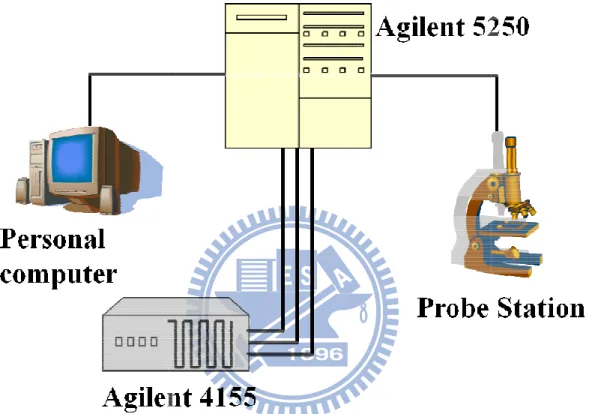
3.2 Measurement Setup and Analysis Method
We use Agilent 4155C to measure the high-κ and metal gate stack CMOS devices with gate length of 30 nm, width of 0.03~0.16 µm and two different EOT 7.8, 12.89Å under an appropriate sampling rate as shown in Fig.3.1.
Fig.3.2 is the flow chart of our analysis process. Fig.3.3 shows a two level RTN pattern with varies gate voltage, ln(τc/τe) becomes smaller as gate voltage increases,
that is, a negative slope can be observed. We measured nMOS with VG=0.4V,
VD=0.1V and VG,step=25mV. As VG increase, the capture time <τc> decreases and
emission time <τe> increases. In other words, the time constant ratio <τc>/<τe>
become smaller when VG increases. We can obtain the slope value, dln(τc/τe)/dVG , is
about -13.426V-1. Since the slope value was smaller than the reference value -27V-1, the vertical trap position can be calculated by Eq.2.5 is 5.79Å in the SiO2 layer and
lateral trap position can be calculated by Eq.2.1 is about 0.4422LDS from source. The
other one is shown in Fig.3.4. On the contrary, As VG increase, the capture time
constant <τc> increases and emission time constant <τe> decreases. Therefore the time
15
dln(τc/τe)/dVG, is about 3.2161V-1. It’s smaller than reference value 12V-1. The trap
positions in vertical and lateral direction are 19.8Å in the HfO2 layer and 0.1462LDS
from source. Finally, we measured 124 nMOS RTN samples and the trap distribution along vertical and lateral direction is shown in Fig.3.5. Most of RTN trap position in vertical direction locates in HfO2 layer. And RTN trap position has a
uniform distribution.
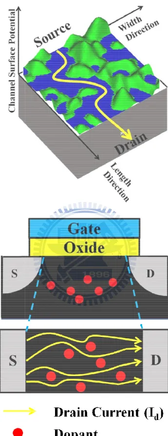
3.3 Percolation Effect
While device technology node scaling down, the number fluctuation can’t explain that RTN amplitudes are different. Therefore, the atomistic random dopant induced percolation effect is proposed. RTN amplitudes in current generation are dominated by percolation effect. Fig.3.6 is the illustration channel surface potential and current pattern at channel surface.[7] The current will percolates through valleys from source to drain. When interface trap trapping a channel carrier, it will generate local potential barrier to disturb the current percolation path. Fig.3.7 shows the current fluctuation result from an interface trap charge at varies positions. If the interface trap charge position locates on the critical current path, then RTN amplitude ∆ID is
relatively large. On the contrary, interface trap charge position locates on the minor percolation path will induce small current fluctuation ∆ID.
Moreover, RTN amplitudes obey exponential distribution and have the following equation [1] [8]: Eq.3.1 1 ( ) exp( d) d I f I σ σ ∆ ∆ = −
16
where σ is distribution standard variation and is a function of doping concentration, cell length, width and oxide thickness. Integrating Eq.3.1, we obtain:
Eq. 3.2
We measured devices with same cell length and controlled different cell width. Fig.3.8 is the RTN amplitude distribution. The distribution standard variation, σ, is increase while cell width is decrease. In other words, cell width is decrease, the interface trap position has higher probability locates on the main percolation path.
( ) exp( d) d I f I σ ∆ ∆ = −
Fig.3.1 Illustration of measurement setup and we use Agilent 4155 to measure
high-κand metal gate stack CMOS devices.
17
Illustration of measurement setup and we use Agilent 4155 to measure and metal gate stack CMOS devices.
18
Fig.3.2 First, focus on a RTN and sweep a wide range of VG with two drain bias VD1
and VD2. Second, obtain the time constant ratio <τc>/<τe> in different VG with VD1.
Third, plot ln(τc/τe) versus VG with VD1, obtain its slope and compare with our
reference points which indicates the trap locates in either HK or IL. Therefore, we can extract the trap vertical position from Table.1. Finally, repeat the steps before with VD2. Then obtain ∆VTS and the trap lateral position can be extracted by Eq.2.1.
Focus on a RTN and sweep a range of
V
Gwith small V
D1and V
D2bias
Analyze RTN and obtain its
ττττ
c/
ττττ
eratio in different V
GPlot ln(
ττττ
c/
ττττ
e) versus V
Gwith V
D1and obtain its slope
→
vertical position
Plot ln(
ττττ
c/
ττττ
e) versus V
Gwith V
D2and obtain its ∆
V
TS19
Fig.3.3 A two level RTN pattern with varies gate voltage, τc becomes smaller as gate
voltage VG increases. ΔVTS is the voltage difference at same time constant ratio.
I
d
(
µµµµ
A
)
Time(s)
V
G=0.4V, V
D=0.1V
0
2
4
6
8
10
2
4
6
y = -13.426x
+ 6.5565
V
D
=-0.1V
V
D
=0.1V
ln
(
ττττ
c
/
ττττ
e
)
V
G
(Volt)
∆
V
TS
0.52
0.56
0.60
0.64
0.68
0.72
-2.0
-1.5
-1.0
-0.5
20
Fig.3.4 A two level RTN pattern with varies gate voltage. Capture time constant τc
becomes larger as gate voltage VG increases.
I
d
(
µµµµ
A
)
Time(s)
0
5
10
5
6
7
V
G(Volt)
ln
(
ττττ
c
/
ττττ
e
)
y=3.2161x
-0.2398
V
D=0.1V
V
D= -0.1V
∆
V
TS0.08
0.12
0.16
0.20
0.24
0.0
0.2
0.4
0.6
21
(a)
(b)
Fig.3.5 (a) is trap distribution along vertical direction. Most of traps locate in HfO2
layer. (b) is trap distribution along lateral direction, which exhibits an uniform distribution.
Vertical position
from channel (X
T/EOT)
N
um
be
rs
SiO
2
HfO
2
0.0
0.2
0.4
0.6
0.8
1.0
0
10
20
30
Total samples:124
N
um
be
rs
0.0
0.2
0.4
0.6
0.8
1.0
0
10
20
30
Total samples:124
Lateral position
Fig.3.6 Illustration of channel surface potential and current pattern.
22
Fig.3.7 When interface trap charge position locates on the main current path, induce large drain current fluctuation
23
When interface trap charge position locates on the main current path, induce large drain current fluctuation ∆Id.
24
Fig.3.8 RTN amplitude distribution with different cell width. σ becomes large as cell
width is decrease.
RTN Amplitude
C
um
ul
a
ti
v
e
P
ro
ba
bi
li
ty
0
1
2
3
4
5
0.01
0.1
1
0.16x0.03
0.08x0.03
0.03x0.03
W
/
L
0.16
/
0.03
0.08
/
0.03
0.03
/
0.03
σ
0.58
0.68
0.94
(
d
)
exp(
I
d
)
f
I
σ
∆
∆
=
−
25
Chapter 4
Analysis of Trap Energy
4.1 Introduction
In this chapter, we demonstrate the extraction of trap energy at zero electric field condition ET0. First of all, we explain that dln(τc/τe)/dVG has different dependences as
VG increases. Second, we derive the trap energy at zero electric field condition ET0; in
other words, extraction of trap energy at flat band condition. Finally, result discussions.
4.2 Cause of V
GDependent Difference
From chapter 3, we know that dln(τc/τe)/dVG has different VG dependences. To
simplify the explanations, we define two types of trap as shown in Fig.4.1. We regard negative and positive VG dependences as Type A trap and Type B trap. Fig.4.2 shows
the band diagram on different VG conditions. From the Fig.4.2, Type A trap exchanges
carriers with channel. Type B trap exchanges carriers with gate electrode. .
4.3 RTN Trap Energy in Flat Band Extraction
Fig.4.3 illustrates nMOS band diagram with a Type A trap in IL layer at different VG biases VFB and VG0.[9] Where XT is trap vertical position from channel, ET is trap
energy, ET0 is ET at zero electric field, Ec is bottom of conduction band, Ev is bottom
26
εSiO2 is dielectric constant of IL layer, εHfO2 is dielectric constant of high-κ layer,
TSiO2 is IL layer thickness, THfO2 is high-κ layer thickness.VG0 is defined as the value
of dln(τc/τe)/dVG is zero. It means that the condition where the trap energy aligns with
Fermi level. To simplify the equations, VSiO2 and VHfO2 are voltage crossed on IL and
high-κ layer respectively and have following equations:
Eq.4.1
Thus the trap energy at zero electric field ET0 can be extracted according to Eq.1.1 and
equation becomes:
Eq.4.2
where k is the Boltzmann’s constant and T is temperature. When VG is equal to VG0,
the Eq.4.2 becomes:
Eq.4.3
Finally, the extraction of trap energy at zero electric field in other conditions listed in Table.2.
Moreover, traps in the triangular area in the ET0 over XT plane can be extracted
by RTN measurement as shown in Fig.4.4.[10] The equipotential line sweeps within this window by varying the applied gate voltage. Fig.4.5 shows the trap energy distribution in common case and our case. The former is measured in strong inversion
2 2 0 SiO SiO 1 ln c T T F s e X E E q V q kT T τ τ = − − − Ψ
(
)
2 2 2 2 2 2 2 SiO SiO 0 0SiO SiO SiO HfO HfO
T T F G FB s s T X E E q V V q T T T ε ε ε − = − − Ψ × + Ψ +
(
)
2 2 2 2 2 2 2 SiO SiO SiO 0SiO SiO HfO HfO G FB s T V V V T T ε ε ε = − − Ψ × +
(
)
2 2 2 2 2 2 2 HfO HfO HfO 0SiO SiO HfO HfO G FB s T V V V T T ε ε ε = − − Ψ × +
27
condition and surface potential variation rate is zero. But the latter was our measurement condition. Most of Type A trap locates within high-κ layer. And Type B trap located within high-κ metal gate interface surface.
It is found that Type B trap is observable when dielectric EOT scaling down as shown in Fig.4.6. Fig.4.7 demonstrates trap energy distribution in two different EOT devices. Type B trap concentrates in a defect band [10]. Thus the traps can be characterized by RTN measurement. It is found that Type B trap is observable due to |VFB| decreases. |VFB| decreases as device dielectric EOT is decrease.[11][12] When
the defect band overlaps the triangle window, the trap can be characterized by RTN measurement. Average of nMOS RTN amplitudes in different types trap as shown in Fig.4.8. The amplitude of Type B trap will induce reliability problem in modern device.
28
Fig.4.1 Definitions of two different types trap. We regard negative and positive VG
dependence as Type A trap and Type B trap.
0.63 0.66 0.69 -1.5 -1.0 -0.5 0.10 0.15 0.20 0.25 0.2 0.4 0.6 y = -13.426x+ 6.5565 ln (ττττcccc //// ττττe ) VG(Volt) y=3.2161x-0.2398 VG(Volt) ln ( ττττcccc //// ττττe )
29
Fig.4.2 Cause of VG dependent difference. Type A traps and Type B traps are interact
with channel and gate electrode respectively.
HfO
2
SiO
2
Metal
Substrate
-exp(
)
c T F eE
E
g
kT
τ
τ
=
Type A
Type B
30
Fig.4.3 Illustrates band diagram about extraction of trap energy at zero electric field
condition ET0. The gate voltage varies from flat band voltage VFB to VG0. When
31
Table.2 is trap energy at zero electric field ET0 in different condition.
(
)
(
)
SiO2 SiO2 0
SiO2 SiO2 HfO2 HfO2 0
HfO2 HfO2 SiO2 0
SiO2 SiO2 HfO2 HfO2 HfO2 g FB s T F s T g FB s T V V T T E E q q T X T V V T T T ε ε ε ε ε ε − − Ψ + + − = + Ψ − − − Ψ +
(
)
(
)
SiO2 SiO2 0SiO2 SiO2 HfO2 HfO2 0
HfO2 HfO2 SiO2
0
SiO2 SiO2 HfO2 HfO2 HfO2
1 g FB s T F s T g FB s T V V T T E E q q T X T V V T T T
ε
ε
ε
ε
ε
ε
− − Ψ − + − = + Ψ − − − Ψ − + (
)
(
)
HfO2 HfO2 0SiO2 SiO2 HfO2 HfO2 0
SiO2 SiO2 0
SiO2 SiO2 HfO2 HfO2 SiO2
1 g FB s T F s T g FB s T V V T T E E q q T X V V T T T ε ε ε ε ε ε − − Ψ + + − = − + Ψ − − Ψ − +
(
)
SiO2 SiO2 0 0SiO2 SiO2 SiO2 HfO2 HfO2
T T F g FB s s
T
X
E
E
q
V
V
q
T
T
T
ε
ε
ε
−
=
−
− Ψ ×
+ Ψ
+
Trap in Oxide interact with channel
Trap in High-k interact with channel
Trap in Oxide interact with gate electrode
32
Fig.4.4 Window on ET0 over XT plane where the trap locates within the window can
be characterized.
Equipotential line
at V
G= V
GHE
GE
T0HfO
2SiO
2Metal
Si
E
cX
TEquipotential line
at V
G= V
GLWindow
(Type A traps)
Window
(Type B traps)
V
GH/V
GL:highest/lowest
V
Gat RTN measurement
33
Fig.4.5 Shows the traps energy distribution in common case and our case. For our
devices, we consider surface potential variation rate.
General case
(Strong inversion)
Our case
(Not strong inversion)
ET 0 -E c (e V )
Vertical Position from Channel
ET 0 -E c (e V )
Vertical Position from Channel dΨS/dVG=0 dΨS/dVG≠0 0.0 0.2 0.4 0.6 0.8 1.0 -1.5 -1.2 -0.9 -0.6 -0.3 0.0 0.3 Type A Type B 0.2V(channel) 0.8V(channel) 0.2V(gate) 0.8V(gate) 0.0 0.2 0.4 0.6 0.8 1.0 -1.5 -1.2 -0.9 -0.6 -0.3 0.0 0.3 Type A Type B 0.2V(channel) 0.8V(channel) 0.2V(gate) 0.8V(gate)
34
Fig.4.6 Shows the number of traps in different EOT devices. Type B traps is
observable when EOT scaling down to 7.8Å.
Type of
RTN traps
Type A
(trap interact
with channel)
Type B
(trap interact
with gate)
EOT=7.8Å
28
10
EOT=12.89Å
37
0
35
Fig.4.7 Type B trap is observable due to |VFB| decreases. Therefore the defect band
overlap the triangle window, Type B trap can be characterized.
EOT=7.8Å case
EOT=12.89Å case
ET 0 -E c (e V )
Vertical Position from Channel
ET 0 -E c (e V )
Vertical Position from Channel
VFB=-0.49V VFB=-0.6V 0.0 0.2 0.4 0.6 0.8 1.0 -1.5 -1.2 -0.9 -0.6 -0.3 0.0 0.3 Type A Type B 0.2V(channel) 0.8V(channel) 0.2V(gate) 0.8V(gate) 0.0 0.2 0.4 0.6 0.8 1.0 -1.5 -1.2 -0.9 -0.6 -0.3 0.0 0.3 Type A Type B 0.2V(channel) 0.8V(channel) 0.2V(gate) 0.8V(gate)
36
Fig.4.8 The average of RTN amplitude of Type B trap is nearly equal to that of Type
A. Type B trap will induce reliability problems in modern devices.
Type of
RTN traps
Type A
(trap interact
with channel)
Type B
(trap interact
with gate)
Average of
RTN amplitude
2.28%
2.064%
37
Chapter 5
Conclusion
A method demonstrated in this thesis to extract trap of position along vertical direction (channel surface to gate electrode) and lateral direction (source to drain). This method can help us to extract the trap profile to device. Moreover, RTN amplitude is dominant by percolation effect. When device EOT becomes thinner, the Type B trap is observable due to |VFB| decreases. Type B trap will induce severe
38
Reference
[1] A. Asenov, Ramesh Balasubramaniam, Andrew R. Brown, and John H. Davies,“RTS Amplitudes in Decananometer MOSFETs: 3-D Simulation Study,” IEEE Trans. Electron Devices, Vol.50, pp. 839 - 845, 2003
[2] Yun Ye, Chi-Chao Wang, Yu Cao, “Simulation of random telegraph Noise with 2-stage equivalent circuit,” in ICCAD, pp. 709 - 713, Nov. 2010.
[3] Hochu Lee, Youngchang YOON, Nonmembers, Seongjae CHO, Student Membern, and Hyungcheol SHIN, Nonmember.C., “Accurate Extraction of the Trap Depth from RTS Noise Data by Including Poly Depletion Effect and Surface Potential Variation in MOSFETs,” in IEICE TRANS. ELECTRON., VOL. E90-C, NO.5 MAY 2007.
[4] Hyungcheol Shin, Byoungchan Oh, ”Characterization of Oxide Traps by RTN Measurement in MOSFETs and Memory Devices,” in IPFA, 2010.
[5] Seungwon YANG, Hochul LEE, and Hyungcheol SHIN, “Simultaneous Extraction of Locations and Energies of Two Indeoendent Traps in Gate Oxide From Four-Level Random Telegraph Signal Noise,” in Japanese Journal of Applied Physics. Vol. 47, No. 4, pp. 2606-2609, 2008.
[6] Sanghoon LEE, Heung-Jae Cho, Younghwan Son, Dong Seup LEE, and Hyungcheol Shin, “Characterization of Oxide Traps Leading to RTN in high-k and Metal Gate MOSFETs,” IEDM Tech, 2009.
[7] Continuum percolation (http://www.ibiblio.org/e-notes/Perc/contour.htm) [8] Koichi Fukuda, Yuui Shimizu, Kazumi Amemiya, Masahiro Kamoshida, and
Chenming Hu, “Random Telegraph Noise in Flash Memories-Model andTechnology Scaling,” IEDM Tech. Dig., pp. 169 - 172, 2007
39
“Statistical Characterization of Trap Position, Energy, Amplitude and Time Constants by RTN Measurement of Multiple Individual Traps,” IEDM Tech. Dig., pp. 628 - 631, 2010
[10] R. Degraeve, M. Cho, B. Govoreanu, B. Kaczer, M.B. Zahid, J. Van Houdt, M. Jurczak, G. Groeseneken, “Trap Spectroscopy by Charge Injection and Sensing (TSCIS): a quantitative electrical technique for studying defects in dielectric stacks,” IEDM Tech. Dig., pp. 1 - 4, 2008
[11] S. Monaghana, P. K. Hurleya, K. Cherkaouia, M. A. Negaraa, and A. Schenkb “Determination of electron effective mass and electron affinity in HfO2 using MOS and MOSFET structures,” in SOLID-STATE ELECTRONICS. Vol.53, No. 4, pp. 438-444, Apr., 2009.
[12] Changhwan Choi, Student Member, IEEE, Chang-Yong Kang, Se Jong Rhee, Student Member, IEEE, Mohammad Shahariar Akbar, Siddarth A. Krishnan, Manhong Zhang, Hyoung-Sub Kim, Tackhwi Lee, Injo Ok, Mohammad Shahariar Akbar, Siddarth A. Krishnan, Manhong Zhang, Hyoung-Sub Kim, Tackhwi Lee, Injo Ok, “Aggressively scaled ultra thin undoped HfO2 gate
dielectric (EOT<0.7 nm) with TaN gate electrode using engineered interface layer,” IEEE Electron Device Lett., vol. 26, no. 7, pp. 454–457, Jul. 2005.