金屬奈米點應用於非揮發性記憶體之製造研究
94
0
0
全文
(2) 誌謝 這份論文的完成不是代表結束,而是進入人生另ㄧ個新的階段。回顧碩士班兩年生 活,良師益友給我學業及生活上最大的鼓勵與支持。首先最要感謝我的指導教授張鼎張 博士,不論在學術領域上的指導,或是在生活上及待人處事方面給我的幫助及啟發,使 學生獲益良多。在此對張老師致上最誠摰的謝意。還要感謝交大顯示所劉柏村教授在實 驗或行政上給予的資源及建議。 此外要特別感謝炳宏學長,他亦師亦友的指導,讓我在學習上完全沒有壓力,並且 給予我極大的實驗自由發展空間,讓我能徹底了解,親身參與整個實驗,這是我在碩士 班期間最大的收穫。還有紀文、土撥、敏全、興華、永俊、世青、致宏、富眀、大山諸 位學長,謝謝你們在我實驗上遭遇難題時給予適時的建議與鼓勵,沒有你們的幫助這篇 論文是無法順利完成的。同時也要特別感謝一起努力的同學雁雅,她總是不厭其煩的教 導進度落後的我做實驗,並且容忍我犯的錯誤給她帶來的不便。永遠笑嘻嘻的臉是實驗 室裡的陽光,寬容的態度是我要學習的最佳榜樣。還要感謝中山物理所的書瑋、光電所 波動實驗室的各位同學,反應遲鈍的我遠在新竹,中山的事務每每麻煩大家幫忙,每次 回來找你們就跟見到老朋友一樣,真的很開心。以及感謝各位在新竹的同學、學弟妹們, 在不屬於我的學校總是麻煩大家照顧了。另外,還要感謝國家奈米實驗室、交大奈米中 心所提供的各項儀器設備和相關資源,使我實驗能順利進行。 最後我要感謝我親愛的母親牛鳳儀女士,我常年在外地求學,母親總是隻身在家, 默默支持著我。我不論何時何地回家,都能感受到無比溫暖,提供我心靈的安寧。並且 包容我的任性,提供我自由的成長和學習空間,使我無後顧之憂的完成我的碩士學位, 她是我心目中最偉大的女性。 謹以此論文獻給所有關心我、幫助過我的人。 陳彥宇 敬上 2005/08/25. i.
(3) 金屬奈米點應用於非揮發性記憶體之製造研究 研究生:陳彥宇. 指導教授:張鼎張 博士 國立中山大學. 光電工程研究所碩士班. 摘要. 近年來,奈米點的應用發展與基礎研究受到相當大的矚目,尤其 當奈米點運用於非揮發性記憶體時,可以解決傳統上利用複晶矽浮停 閘做為載子儲存單元的非揮發性記憶體(例如,快閃記憶體)之元件微 縮問題,例如:在經過多次資料讀取與寫入過程中所造成的穿隧氧化 層漏電路徑,將使得儲存單元中的電荷全部流失,造成記憶體元件功 能的失效。因此在元件微縮過程中,穿隧氧化層的厚度將成為限制了 元件微縮的重要關鍵之一。再者由於穿隧氧化層無法薄化,於是操作 電壓也無法降低,讀取速度也跟著無法增快,這些問題也深深影響著 非揮發性記憶體的應用性。但若以奈米點取代浮停閘結構可以解決上 述問題,因為電荷僅儲存於分離的奈米點中,若穿隧氧化層存在局部 的漏電路徑,並不會導致電荷的全部流失,仍能維持記憶元件之功能。 金屬奈米點的特色主要有高狀態密度、強通道耦合能力、可調變. ii.
(4) 金屬功函數以及不易受載子侷限效應所引起的能階擾動。在元件設計 上金屬奈米點不但可減少操作電壓、增加抹除寫入速度與電子保存時 間。本論文主要以金屬鈷以及鈷的矽化物作為記憶體儲存元件材料來 作研究,利用高溫爐管氧化、快速退火等各項條件形成奈米點,並用 材料分析與電性分析來研究奈米點的電荷儲存效應。. iii.
(5) Study on the Fabrication of Non-volatile memory with Metal Nanocrystals Student: Yan-Yu Chen. Advisor: Ting-Chang Chang. Institute of Electrical Optical Engineering National Sun Yat-Sen University. Abstract. In recent years, the fundamental researches on nanocrystals have been received increasing attentions for the novel applications, especially the nonvolatile memory technology. Adoption of nanocrystals technology could solve the serious limitation suffered by the conventional nonvolatile memory, flash, while scaling down. Once the thin tunneling oxide of flash device has been created a leaky path, all the stored charge in the floating gate will be lost after numerous counts of data reading and writing. Hence, the thinning of tunneling oxide will become one of important keys to the scaling limitation. Furthermore, if the tunneling oxide can not be thinned any more, both the operation voltage and speed of memory can not be improved. These drawbacks will restrict the development of nonvolatile memory. Replacement of floating gate structure with nanocrystals could effectively avoid the data losing due to the leaky path in the thin tunneling oxide. All stored charges can’t be lost through the few leaky iv.
(6) paths since the charges are stored in distributed nanocrystals. The charges stored nearby the leaky path will be lost, but others are still kept in the distributed and independent nanocrystals. The advantages of metal nanocrystals has have higher density of states around Fermi level, stronger coupling with conduction channel, wide range of available work functions and smaller energy perturbation due to carrier confinement. So metal nanocrystals can reduce operate voltage, and increase write/erase speed and endurance. In this thesis, we will study of cobalt and cobalt-silicide as the memory storage element. The nanocrystals were formed by high temperature oxidation or metal rapid thermal annealing with all kinds of conditions. And we analyze the effect of electron storage at metal nanocrystals by means of material and electrical analysis.. v.
(7) Contents. Acknowledgment………………………………………………………...i Chinese Abstract……………………………………………...................ii English Abstract………………………………………………………..iv Contents…………………………………………………………………vi Table Captions………………………………………………………….ix Figure Captions.........................................................................................x. Chapter 1 Introduction 1.1 General Background………………………………………….…1 1.1.1 SONOS nonvolatile memory devices……………………..3 1.1.2 Nanocrystal nonvolatile memory devices (semiconductor nanocrystals)…………………………….5 1.1.3 Nanocrystal nonvolatile memory devices (metal nanocrystals)…………………………………..…10 1.2 Motivation……………………………………………………..12 1.3 Organization of the dissertation………………………………..13. Chapter 2 Characteristic of Cobalt -Silicide Nanocrystals Memories Structures with Different Fabrication processes 2.1 Introduction…………………………………………………....15 vi.
(8) 2.2 Experimental procedures………………………………………17 2.2.1 The Oxidation of the Dry Oxide/Cobalt/amorphous Silicon Structure…………………………………………………17 2.2.2 The Oxidation of the Dry Oxide/Cobalt/amorphous Silicon/Silicon Dioxide/amorphous Silicon Structure…..18 2.2.3 The Oxidation of the Dry Oxide/Cobalt/amorphous Silicon/TEOS Oxide Structure…………………………..20 2.3 Results and discussions………………………………………..22 2.3.1 The Material Characteristic and Electrical Characteristics of the Dry Oxide/Cobalt/amorphous Silicon Structure…22 2.3.2 The Material Characteristic and Electrical Characteristics of the Dry Oxide/Cobalt/amorphous Silicon/Silicon Dioxide/amorphous Silicon Structure………………..….23 2.3.3 The Electrical Characteristics of the Dry Oxide/Cobalt/amorphous Silicon/TEOS Oxide Structure……………………………………………..…..25 2.4 Summary…………………………………………………….....26. Chapter 3 A Novel Approach of Fabricating Cobalt Nanocrystals for Nonvolatile Memory Application 3.1 Introduction…………………………………………………....28 3.2 Experimental procedures……………………………………....29 3.2.1 The Annealing of the Dry Oxide/Cobalt/ TEOS Oxide Structure…………………………………………………29. vii.
(9) 3.2.2 The Oxidation of the Dry Oxide/Cobalt/ TEOS Oxide Structure…………………………………………………31 3.3 Results and discussions…………………………………......…33 3.3.1 The Electrical Characteristics of the Annealing of the Dry Oxide/Cobalt/ TEOS Oxide Structure…………………..33 3.3.2 The Electrical Characteristics of the Oxidation of the Dry Oxide/Cobalt/ TEOS Oxide Structure…………………..34 3.4 Summary…………………………………………………….....34. Chapter 4 Novel design of Cobalt -Silicide Nanocrystals Structures with Nanosphere Template Technology 4.1 Introduction………………………………………………..…..35 4.2 Experimental procedures…………………………………..…..35 4.3 Results and discussions………………………………….....….37 4.4 Summary………………………………………………..……...38. Chapter 5 Conclusions and Suggestion for Future Work 5.1 Conclusions………………………………………………....…39 5.2 Suggestion for Future Work……………………………..……..40. Reference…………………………………………………………….....42 Note………………………………………………………………...…...47. viii.
(10) Table Captions. Chapter 2: Table 2.2.1 Experimental parameters of the Dry Oxide/Cobalt/amorphous Silicon Structure. Table 2.2.2 Experimental parameters of the Dry Oxide/ Cobalt /amorphous Silicon/ Silicon Dioxide/amorphous Silicon Structure. Table 2.2.3 Experimental parameters of the Dry Oxide/ Cobalt /amorphous Silicon/TEOS Oxide Structure.. Chapter 3: Table 3.2.1 Experimental parameters of the Dry Oxide/ Cobalt / TEOS Oxide Structure. Table 3.2.2 Experimental parameters of the Dry Oxide/ Cobalt / TEOS Oxide Structure.. ix.
(11) Figure Captions. Chapter 1: Figure 1.1-1 The structure of the conventional floating gate nonvolatile memory device. Continuous poly-Si floating gate is used as the charge storage element. Figure 1.1-2 The structure of the SONOS nonvolatile memory device. The nitride layer is used as the charge-trapping element. Figure 1.1-3 The structure of the nanocrystal nonvolatile memory device. The semiconductor nanocrystals or metal nano-dots are used as the charge storage element instead of the continuous poly-Si floating gate. Figure 1.1.1-1 The energy band diagrams of the write/erase operation for a nanocrystal NVSM device. Figure 1.1.2-1 The development of the gate stack of SONOS EEPROM memory devices. The optimization of nitride and oxide films has been the main focus in recent years. Figure 1.1.3-1 band diagram illustration of different approaches for improving the Jg,programming/erase/Jg,retention ratio.. Chapter 2: Figure 2.2.1 Process flow of the Dry Oxide/Cobalt/amorphous Silicon Structure. Figure 2.2.2 Process flow of the Dry Oxide/ Cobalt /amorphous Silicon/ Silicon Dioxide/amorphous Silicon Structure. Figure 2.2.3 Process flow of the Dry Oxide/ Cobalt /amorphous Silicon/TEOS x.
(12) Oxide Structure. Figure 2.3.1-1(a) Standard of the Dry Oxide/Cobalt/amorphous Silicon Structure before oxidation. Figure 2.3.1-1(b) The Dry Oxide/Cobalt/amorphous Silicon Structure after oxidation at 900°C 10min. Figure 2.3.1-2(a) The C-V hysteresis loop of cobalt-silicide nanocrystals in samples oxidized at 900°C 10min. Figure 2.3.1-2(b) The C-V hysteresis loop of cobalt-silicide nanocrystals in samples oxidized at 900°C 10min. Figure 2.3.1-2(c) The C-V hysteresis loop of cobalt-silicide nanocrystals in samples oxidized at 850°C 10min. Figure 2.3.1-2(d) The C-V hysteresis loop of cobalt-silicide nanocrystals in samples oxidized at 800°C 10min. Figure 2.3.2-1 The Dry Oxide/ Cobalt /amorphous Silicon/ Silicon Dioxide/amorphous Silicon Structure after oxidation at 800°C 10min. Figure 2.3.2-2(a) The plan-view TEM image of Dry Oxide/ Cobalt /amorphous Silicon/ Silicon Dioxide/amorphous Silicon Structure after 800 °C oxidation. Figure 2.3.2-2(b) The size distribution of the nanocrystals. Figure 2.3.2-3(a) The C-V hysteresis loop of cobalt-silicide nanocrystals in samples oxidized at 800°C 10min with 6V programming voltage. Figure 2.3.2-3(b) The C-V hysteresis loop of cobalt-silicide nanocrystals in samples oxidized at 800°C 10min with 3V programming voltage. Figure 2.3.2-4 The band diagrams of “write” and “erase” operations of the memory device.. xi.
(13) Figure 2.3.3-1(a) The C-V hysteresis loop of cobalt-silicide nanocrystals in samples annealing at 800°C 100sec with 8V programming voltage. Figure 2.3.3-1(b) The C-V hysteresis loop of cobalt-silicide nanocrystals in samples annealing at 800°C 100sec with 10V programming voltage.. Chapter 3: Figure 3.1-1 Self-assembled phenomenon of metal nanocrystals. Figure 3.2.1 Process flow of the Dry Oxide/ Cobalt /TEOS Oxide Structure. Figure 3.2.2 Process flow of the Dry Oxide/ Cobalt /TEOS Oxide Structure. Figure 3.3.1-1 The C-V hysteresis loop of cobalt nanocrystals in samples annealing at 900°C 60sec with 4V programming voltage. Figure 3.3.1-2 The band diagrams of “write” and “erase” operations of the memory device. Figure 3.3.2 The C-V hysteresis loop of cobalt nanocrystals in samples oxidized at 900°C 10min with 8V programming voltage.. Chapter 4: Diagram 4.2-1 The sample that macromolecule nanosphere template be spun on the substrate. Diagram 4.2-2 The sample after purge the macromolecule nanosphere template. Figure 4.2-3 Process flow of the Dry Oxide/ Cobalt /TEOS Oxide Structure with Nanosphere Template. Figure 4.3-1 Triangles of cobalt that be deposited in the interval of the nanosphere was observed clearly. xii.
(14) Figure 4.3-2(a) Plan-view of the sample after annealing. Figure 4.3-2(b) Plan-view of the sample after annealing. Figure 4.3-3 The C-V hysteresis loop of cobalt nanocrystals in samples annealing at 400°C 60sec with 4V programming voltage. Figure 4.3-4 The C-V hysteresis loop of cobalt nanocrystals in samples annealing at 400°C 60sec with 8V programming voltage.. xiii.
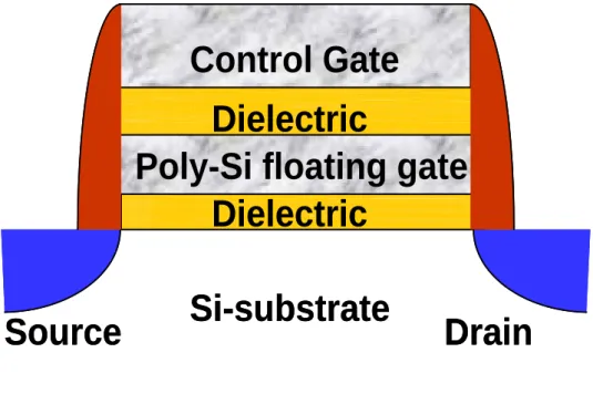
(15) Chapter 1. Introduction. 1.1 General Background. In early years, magnetic-core memory is master stream. In 1960’s, due to the high cost, large volume, and high power consumption of the magnetic-core memory, the electronic industries urgently needed a new kind of memory device to replace the magnetic-core memory. In 1967, D. Kahng and S. M. Sze invented the floating-gate (FG) nonvolatile semiconductor memory at Bell Labs [1.1]. A standard Conventional Flash device, similar to the Intel ETOX (EPROM Tunnel Oxide) structure, as shown in Figure 1.1-1. The basic device is a Metal-Oxide-Semiconductor Field Effect Transistor (MOSFET) with a modified gate stack structure that has a control gate (CG) and a floating gate (FG) embedded in a dielectric material such as silicon dioxide (SiO2). The first SiO2 energy barrier between the floating gate and the channel prevents electrons from leaking into the channel. The second barrier between the floating gate and the control gate prevents electrons from escaping to the control gate. The operation principal is using the floating gate to be the charge stored units. After electrons which injected from the channel stored in floating gate, the threshold voltage of devices will be changed. The logical “0” and “1” definition of nonvolatile memory devices are used for the difference between threshold voltages. The invention of FG memory impacts more than the replacement of magnetic-core memory, and creates a huge industry of portable electronic systems. The stacked-gate FG device 1.
(16) structure continues to be the most prevailing nonvolatile-memory implementation, and is widely used in both standalone and embedded memories up to today. The most widespread memory array organization is the so-called Flash memory, which has a byte-selectable write operation combined with a sector “flash” erase. Although a huge commercial success, conventional FG devices still come to be in face of their limitations. The most prominent one is the limited potential for continued scaling down of vertical stack structure. This scaling limitation stems from the extreme requirements put on the tunnel oxide layer. Since the SiO2 barrier between the floating gate and the MOSFET channel is very thin, its quality is critical to ensure good floating gate isolation. Unfortunately, defects due to the structural imperfections and atomic bonding are unavoidable in realistic materials. These defects allow for leakage paths that are detrimental to charge storage in the floating gate. Once the tunnel oxide has been created a leaky path, all the stored charge in the floating gate will be lost. When the tunnel oxide is thinner for the consideration, the retention characteristics may be degraded. And when the tunnel oxide is made thicker to take the isolation into account, the speed of the operation will be slower. On the one hand, the tunnel oxide has to allow quick and efficient charge transfer to and from the FG. On the other hand, the tunnel oxide needs to provide superior isolation under retention, endurance, and disturbed conditions in order to maintain information integrity over periods of up to a decade. Therefore, there is a tradeoff between speed and reliability and the thickness of the tunnel oxide is compromised to about 8-11 nm, which is barely reduced over more than five successive generations of the industry [1.2]. To overcome the scaling limits of the conventional FG structure, two candidates are mostly mentioned, SONOS [1.3-1.5] and nanocrystal nonvolatile memory devices [1.6-1.8]. As for SONOS in Fig. 1.1-2, the nitride layer is used as the charge-trapping. 2.
(17) element. The intrinsic distributed storage takes an advantage of the SONOS device over the FG device, its improved endurance, since a single defect will not cause the discharge of the memory [1.5]. Tiwari et al. [1.6] for the first time demonstrated the silcon nanocrystal floating gate memory device in the early nineties. As shown in Fig. 1.1-3, the local leaky path will not cause the entire loss of information for the nanocrystal nonvolatile memory device. Also, the nanocrystal memory device can maintain good retention characteristics when tunnel oxide is thinner and lower the power consumption [1.6-1.8]. The term “endurance” refers to the ability of the NVSM to withstand repeated program cycles and still meet the specification in the data sheet. The term “retention” describes the ability of the NVSM to store and recover information after a number of program cycles at a specified temperature.. 1.1.1 SONOS nonvolatile memory devices. The. triple-dielectric. polysilicon-blocking. oxidesilicon. nitride-tunnel. oxide-silicon (SONOS) structure is an attractive candidate for high density EEPROM’s suitable for semiconductor disks and as a replacement for high-density dynamic random access memories (DRAM’s). Low programming voltages (5 V) and high endurance (greater than 107 cycles) are possible in this multidielectric technology as the intermediate Si3N4 layer is scaled to thicknesses of 50Å. Oxide thickness in this range is necessary to minimize the undesirable effects of gate disturb while still enabling a low-voltage operation to maximize the cost benefit of SONOS memories. The thin gate insulator and low programming voltage enable the scaling of the basic memory cell and associated complementary metal-oxide-semiconductor (CMOS) peripheral circuitry on the memory chip. 3.
(18) Advancements in ultra-thin tunnel oxides during the 1990s have opened the path to improve performance and reliability for NVSMs based on SONOS technology [1.9]. The optimization of nitride and oxide films has been the main focus in recent years. Initial device structures in the early 1970s were p-channel metal-nitride-oxide-silicon (MNOS) structures with aluminum gate electrodes and thick (45 nm) silicon nitride charge storage layers. Write/erase voltages were typically 25-30 V. In the late 1970s and early 1980s, scaling moved to n-channel SNONS devices with write/erase voltages of 14-18 V. In the late 1980s and early 1990s, n- and p-channel SONOS devices emerged with write/erase voltages of 5-12 V. Figure 1.1.1-1 illustrates the write/erase operation using an energy-band diagram. The electrons injected from the channel are trapped in the forbidden gap of the silicon nitride film. The electrons, which are not trapped in the nitride film, tunnel through the blocking oxide into the gate electrode. If the poly-Si gate is doped p+, then holes may tunnel from the gate to the silicon nitride valence band, thereby compensating the trapped electrons and reducing the threshold voltage shift. During the erase operation, holes are injected from the substrate into the silicon nitride valence band where they are trapped in a manner similar to electrons. The free holes pile up at the blocking oxide interface because of the larger barrier height (5eV). Electrons may tunnel from the gate electrode into the nitride compensating the injected holes. A larger barrier for holes (4.7 eV) requires tunnel oxides to be less than 2.5 nm for efficient tunneling and, therefore, “hole tunneling” depends strongly on the tunnel oxide thickness. Additionally, electrons may tunnel from the valence band of the gate electrode; however, the barrier height for this process is increased by the silicon bandgap (1 eV) as compared with the tunneling from the conduction band. Thus, in summary, for SONOS device operation both carrier types are involved in the transport process. Low-voltage (5-10 V) SONOS NVSMs may be scaled in cell size to 6F2 (F=feature 4.
(19) size) and perhaps even smaller in the years to come. The simplified ONO gate stack in SONOS memory transistors lends itself to the economics of scaled CMOS circuits. The compatibility of SONOS technology with advanced CMOS logic technology permits economical integration of NVSMs as embedded EEPROMs in ASIC chips. Finally, radiation hardness provides a unique and important feature for advanced military and space systems.. 1.1.2. Nanocrystal. nonvolatile. memory. devices. (semiconductor. nanocrystals). The charge storage property of semiconductor nanocrystals embedded in a silicon oxide matrix is currently under intense investigation due to its potential application in future nonvolatile memories. The continuous down scaling of device dimensions requires more stringent and better controlled fabrication processes. One way to conveniently achieve nanometer range structures without sophisticated nanolithography techniques is through the synthesis of nanocrystals. However, the charges loss through lateral paths in nanocrystal-based memory devices can be suppressed by the oxide isolation between nanocrystals, these devices exhibited superior charge storage characteristics compared with conventional floating-gate memory devices. All stored charges can’t be lost through the few leaky paths since the charges are stored in distributed nano-dots. One way to alleviate the scaling limitation of the conventional FG device, while still preserving the fundamental operating principle of the memory, is to rely on distributed charge storage instead. The typically investigations are used semiconductors (Si or Ge) as nano dot to reduce the tunneling oxide of thickness without losing its reliability and further to reduce operation 5.
(20) voltage. Nanocrystal nonvolatile memories first introduced in the early 1990s. In a nanocrystal NVSM device, charge is not stored on a continuous FG poly-Si layer, but instead of a layer of discrete, mutually isolated, crystalline nanocrystals or dots. Each dot will typically store only a handful of electrons; collectively the charges stored in these dots control the channel conductivity of the memory transistor. Figure 1.1.2-1 illustrates the progression of device cross section, which has led to the present nanocrystal NVSM device structure. As compared to conventional stacked gate NVSM devices, nanocrystal charge storage offers several advantages, the main one being the potential to use thinner tunnel oxide without sacrificing nonvolatility. This is a quite attractive proposition since reducing the tunnel oxide thickness is a key to lowering operating voltages and/or increasing operating speeds. This claim of improved scalability results not only from the distributed nature of the charge storage, which makes the storage more robust and fault-tolerant, but also from the beneficial effects of Coulomb blockade [1.7]. Quantum confinement effects (bandgap widening; energy quantization) can be notable of small nanocrystal geometries (sub-3 nm dot diameter) to further enhance the memory’s performance. There still keep the other important advantages. First, the fabrication of the nanocrystal memories is more simplified and lower cost process as compared to conventional stacked-gate Flash memories. Second, due to the absence of drain to FG coupling, nanocrystal memories suffer less from drain induced barrier lowering (DIBL) so they have intrinsically better punch through characteristics. This advantage is gained a higher drain bias during the read operation, thus improving memory access time. Alternatively, it allows the use of shorter channel lengths and therefore smaller cell area. Third, nanocrystal memories are characterized by excellent immunity to 6.
(21) stress induced leakage current (SILC) and oxide defects due to the isolated charge storage in the nanocrystal layer. However, the other is the low capacitive coupling between the external control gate and the nanocrystal charge storage layer. This does not only results in lower operating voltages, thus offsetting the benefits of the thinner tunnel oxide, it also removes an important design parameter (the coupling ratio) typically used to optimize the performance and reliability tradeoff. As for the fabrication processes, a first requirement is the aerial density of the nanocrystal dots. A typical target is a density of at least 1012 cm-2. This is equivalent to approximately 100 particles controlling the channel of a memory FET with 100×100 nm2 active area, and requires particle size of 5-6 nm and below. Second, the fabrication process should result in a planar nanocrystal layer, i.e., the thickness of the dielectric layer separating the nanocrystal and the substrate should be well controlled. Poor control of the tunnel oxide thickness will result in wider threshold voltage distributions and will increase the number erratic bits. More generally, good process control is needed with regards to such nanocrystal features as: size and size distribution, inter-crystal interaction (lateral isolation), uniformity of aerial crystal density, and crystal doping (type and level). Recently, Lombardo et al. demonstrated the nucleation process is not purely random and the dots forms with partial self-ordering. The relative dispersion of Rdot is numerically evaluated as a function of gate size, both for random and partially self-ordered nucleation processes [1.10]. A theoretical model considering quantum confinement and Coulomb blockade in lower Si dot shows that charge retention is improved exponentially by lower dot size scaling. As the size and size distribution of the Ge nanocrystals have been considered, She et al. [1.11] made a conclusion on Ge nanocrystal memory device that nanocrystal size around 5 nm is preferred to achieve fast programming speed and longer retention time, and the size should not be scaled below that. The quantum confinement effect for Ge 7.
(22) nanocrystals smaller than 5 nm is very significant so that the retention time is shorter and the programming time is longer. Finally, it is preferred that the fabrication process is simple and that it uses standard semiconductor equipments. Several nanocrystal fabrication processes have been demonstrated. Numerous efforts have focused on obtaining a high density of nanocrystals through a variety of techniques including aerosol technique, ion implantation, MBE technique, direct chemical vapor deposition (CVD) and recrystallization anneal of amorphous-Si. Kim et al. used conventional LPCVD reactor to fabricate Si nanocrystals at 620 ℃ [1.12]. Direct CVD of silicon is preferred over ion implantation and recrystallization anneal due to the difficulty in obtaining the required amount of Si in the stack. Further, nucleation and growth by CVD provides appropriate simpler processing controls to manipulate the size and density of nanocrystals. Si nanocrystals with number density between 1011 and 1012/cm2 have been deposited on various dielectrics such as SiO2, Si3N4 and Al2O3 using CVD. A high density of about 5×10¹¹/cm2 was obtained on nitride surface, and the density was more than three times larger than that on oxide [1.13-1.14]. Fernandes et al. acquired the higher density Si quantum dots (~1012/cm2) by integrating on SiO2/ALD Al2O3 tunneling dielectrics [1.15]. Kanjilal et al. demonstrated a sheet of spherical, well-separated, crystalline Ge nanodots embedded in SiO2 on top of. p-(001) Si wafer, fabricated by molecular beam epitaxy (MBE). combined with rapid thermal processing and characterized structurally and electrically [1.16]. To fabricate Ge nanocrystals, the oxidation of SiGe contained films has been utilized [1.17]. As the SiGe layer is oxidized, the Ge element will be downward segregated and Si will be oxidized into SiO2 [1.18-1.19]. Ostraat et al. proposed an aerosol silicon nanocrystal nonvolatile memory device with large threshold voltage shift (>3V), sub-microsecond program times, millisecond erase times, excellent endurance (>105 program/erase cycles), and long term nonvolatility (>106 sec) 8.
(23) [1.20]. Qu et al. presented an approach for synthesizing Ge nanocrystals embedded in amorphous silicon nitride films [1.21]. On the basis of preferential chemical bonding formation of Si-N and Ge-Ge, thin films with Ge clusters embedded in amorphous silicon nitride matrix have been prepared by plasma enhanced chemical vapor deposition (PECVD) with reactant gases of SiH4, GeH4, and NH3 mixed in hydrogen plasma at 250 ℃. Park et al. also utilized PECVD to form Si nanocrystals embedded in silicon nitride film [1.22]. They presented the electron charging and discharging effects of the Si nanocrystals embedded in SiNx film. Capacitance-voltage hysteresis is used to inspect the memory effects of the nanocrystal memory devices [1.23]. Differing from the required single planar nanocrystal layer, Ohba et al. proposed a novel Si dot memory whose floating gate consists of self-aligned doubly stacked Si dots. A lower Si dot exists immediately below an upper dot and lies between thin tunnel oxides. It is experimentally shown that charge retention is improved compared to the usual single layer Si dot memory [1.24]. As for the tunnel dielectric for the nanocrystal nonvolatile memory devices, Baik et al. proposed a tunnel barrier structure that is composed of silicon dioxide and amorphous carbon (a-C) to attain enhanced charge retention without degradation in the injection efficiency. Additionally, high-k tunnel dielectrics were investigated for Si nanocrystal memory devices [1.25-1.27]. Results show that due to its unique band asymmetry in programming and retention mode, the use of high-k dielectric on Si channel offers lower electron barrier height at dielectric/Si interface and larger physical thickness, results in a much higher Jg,programming/Jg,retention ratio than that in SiO2 and therefore faster programming and longer retention. The programming is considered as the electron injection from the channel under positive bias operation for an NMOSFET memory device. However, the programming and erasing mechanisms of p-channel nanocrystal memory devices were also investigated by Han et al. [1.28]. 9.
(24) Promising device results have been presented, demonstrating low-voltage operation for comparable threshold voltage windows and operating speeds, and thin tunnel oxide retention behavior that suggests meeting long-term nonvolatility requirements. In spite of these promising results, it is unclear whether nanocrystal memories will ever see commercialization. In order for that to happen, the uniformity of the nanocrystals needs to be improved, and the claimed benefits need to be more unambiguously substantiated.. 1.1.3 Nanocrystal nonvolatile memory devices (metal nanocrystals). In optimizing the memory devices, the ideal goal is to achieve the fast write/erase of DRAM and the long retention time of Flash memories simultaneously. For this purpose we need to create an asymmetry in charge transport through the gate dielectric to maximize the Jg,programming/Jg,retention ratio. Three different approaches for achieving this goal are illustrated in Fig. 1.1.3-1. By replacing the rectangular barrier with a parabolic or triangular barrier, the barrier height can be modulated by the electric field in the tunnel oxide [1.29]. Therefore, a higher tunnel–barrier is present during retention as the low electric field and a lower barrier is present during write/erase operations as the high electric field induced by external bias, thus increasing the Jg,programming/Jg,retention ratio. In practice, the parabolic or triangular barrier can be simulated by stacking multiple layers of dielectrics. Another approach is to use double-stacked storage nodes, preferably self-aligned with smaller dots at the lower stack [1.30]. In such devices, fast write/erase can still be achieved, if sufficiently thin tunnel oxides are used below and between the two stacks. However, the retention time can be significantly improved due to the Coulomb blockade effect at the lower stack, 10.
(25) which prevents electrons in the top stack storage nodes from tunneling back into the substrate. The third approach is to engineer the depth of the potential well at the storage nodes, thus creating an asymmetrical barrier between the substrate and the storage nodes, i.e., a small barrier for writing and a large barrier for retention. This can be achieved if the storage nodes are made of metal nanocrystals. Then by engineering the metal work function, the barrier height can be adjusted by about 2 eV, giving much freedom for device optimization. In addition to semiconductor nanocrystals, Liu et al. described the design principles and fabrication processes of metal nanocrystals [1.31-1.32]. The metal nanocrystal memory is exhibited to several advantages, such as stronger coupling with the conduction channel, better size scalability, higher density of states around the Fermi level, smaller energy perturbation due to carrier confinement, and the design freedom of engineering the work functions to optimize the device characteristics. In addition, the nanocrystals do not bear a voltage drop from gate voltage, which means all the voltages provided from control gate are dropped to tunnel oxide and control oxide and gains advantage. The higher density of states makes metal nanocrystals more immune to Fermi-level fluctuation caused by contamination. The metal nanocrystals tend to have more uniform charging characteristics, resulting in tighter Vth control. The wide range of available work functions provides one more degree of design freedom to engineer the tradeoff between write/erase and charge retention because the work function of nanocrystals affects both the depth of the potential well at the storage node and the density of states available for tunneling in the substrate. By aligning the nanocrystal Fermi level to be within the Si bandgap under retention and above the conduction band edge under erase, a large Jg,erase/Jg,retention ratio can be achieved even for very thin tunnel oxides. Because writing is performed by tunneling electrons from the Si substrate into the nanocrystals (thus can always find available 11.
(26) states to tunnel into) and can have current level similar to Jg,erase , fast write/erase and long retention time can be achieved simultaneously in metal nanocrystal memories. Metal nanocrystals also provide a great degree of scalability for the nanocrystal size. To enable single-electron or few-electron memories by the Coulomb blockade effect, smaller nanocrystals are preferred. However, for semiconductor nanocrystals, the band-gap of nanocrystals is widened in comparison with that of the bulk materials due to the multidimensional carrier confinement, which reduces the effective depth of the potential well and compromises the retention time. This effect is much smaller in a metal nanocrystal because there are thousands of conduction-band electrons in a nanocrystal even in charge neutral state. As a result, the increase of Fermi level is minimal for metal nanocrystals of nanometer size.. 1.2 Motivation. In recent years, the portable electronic product have widely applied, such as digit camera, notebook computer, mp3 walkman, intelligent IC card, USB Flash personal disc ,etc., and play an important role in the market. These products all are based on flash memory. The demand for the flash memory device grows with each passing day, the density and operation speed of flash memory and its reliability become the popular research theme. Recently, the memories are required by the high density, fast operation speed and good reliability. Memory-cell structures employing discrete traps as the charge storage media have attracted large of the researches as the promising candidates to replace conventional DRAM or Flash memories. Considerable attention has been focused on semiconductor or metal nanocrystals embedded in the silicon dioxide of a metal oxide 12.
(27) semiconductor (MOS) device for future high speed and low power consuming memory device [1.6][1.33]. The self-assembling of silicon or germanium nanocrystals embedded in SiO2 layers has been widely studied, and strong memory effect in MOS devices were reported [1.8][1.34][1.35]. The metal nanocrystals memories come into notice as so many advantages. The advantages of metal nanocrystals over their semiconductor counterparts include low power consumption, high density of states around the Fermi level, stronger coupling with the channel, better size scalability, smaller energy perturbation due to carrier confinement [1.33], and the design freedom of engineering the work functions to optimize device characteristics. A self-assembled nanocrystal formation process by rapid thermal annealing of ultra thin metal film deposited on top of tunnel oxide is developed and integrated with NMOSFET devices. Due to the minimization of the surface energy of the metal film under rapid thermal annealing, the driving force results in a discrete layer of metal nanodots reside on tunnel oxide. Our researches were chosen Cobalt/Cobalt Silicide as the main materials. The reasons why Cobalt/Cobalt Silicide were chosen as the materials for the nanocrystals are the compatibility with current manufacturing technology of semiconductor industry, and thermal stability of the Cobalt Silicide.. 1.3 Organization of the dissertation. This dissertation is divided into five chapters. The contents in each chapter are described as follows. In chapter 1, the potential memory devices about Conventional Flash, SONOS and Nanocrystal memory devices is introduced. 13.
(28) In chapter 2, the study on cobalt silicide (CoSi2) nanocrystal memories technology by three different methods is investigated. First, cobalt silicide nanocrystal was fabricated by one step (to formed nanocrystals and oxidized amorphous silicon to dioxide at the same time) process. Then, the others methods were proposed to improve the diffusion phenomenon of cobalt silicide at the first method. Final, we will discuss and compare with the device characteristics between different methods and conditions. In chapter 3, the study on Cobalt nanocrystal memory using Dual E-Gun Evaporation System deposited Cobalt thin film is investigated. Then, we will discuss the characteristics between different conditions. In chapter 4, a new method of fabricating cobalt silicide nanocrystals is introduced. The nanosphere template technology will be utilized for obtaining well-order 2-D array nano-dots. Moreover, the comparison in electrical properties between random and regular arrangements of nano-dots in space will be characterized. In chapter 5, the conclusions of all experimental results in this dissertation and suggestions for the future research will be descried in this chapter. Final, there are some matters needing attention in the experiment.. 14.
(29) Chapter 2. Characteristic of Cobalt -Silicide Nanocrystals Memories Structures with Different Fabrication processes. 2.1 Introduction. Metal nanocrystal charge storage offers several potential advantages over conventional stacked-gate nonvolatile memory devices include higher density of states around the Fermi level, stronger coupling with the conduction channel, a wide range of available work functions, and smaller energy perturbation due to carrier confinement. The higher density of states makes metal nanocrystals more immune to Fermi-level fluctuation caused by contamination. The metal nanocrystals tend to have more uniform charging characteristics, resulting in tighter control. The wide range of available work functions provides one more degree of design freedom to engineer the tradeoff between write/erase and charge retention because the work function of nanocrystals affects both the depth of the potential well at the storage node and the density of states available for tunneling in the substrate. By aligning the nanocrystals Fermi level to be within the silicon band-gap under retention and above the conduction band edge under erase, a large can be achieved even for very thin tunnel oxides. Because writing is performed by tunneling electrons from the silicon substrate into the nanocrystals thus can always find available states to tunnel into and can have current level similar to, fast write/erase and long retention time can be achieved. 15.
(30) simultaneously in metal nanocrystals memories. Metal nanocrystals also provide a great degree of scalability for the nanocrystals size. To enable single-electron or few-electron memories by the Coulomb blockade effect, smaller nanocrystals are preferred. However, for semiconductor nanocrystals, the band-gap of nanocrystals is widened in comparison with that of the bulk materials due to the multidimensional carrier confinement, which reduces the effective depth of the potential well and compromises the retention time. This effect is much smaller in metal nanocrystals because there are thousands of conduction-band electrons in nanocrystals even in charge neutral state. As a result, the increase of Fermi level is minimal for metal nanocrystals of nanometer size. As the scaling down the size of device in very large scale integrated circuits (VLSI) technology, silicides generally apply to any aspect such as lower contact resistance and fully silicide (FUSI) metal gate [2.1]. Most important of all, some reports indicate that silicide has self-passivating silicon dioxide formed under high oxidation temperature or prolonging heat treatment time [2.2]. At the same time, silicide films tended to agglomerate or form islands under such annealing condition. According to these reason, we employed this phenomenon to manufacture our metal nanocrystals embedded in the SiO2 layer. Furthermore we verified this method could have effect of memory. And this method was one step process that we can form not only the memory storage medium but also the control silicon dioxide. This process can be so simpler low cost fabrication process than traditional nanocrystal memories processes. However, we wanted to research in the storage characteristics of the Nickel Silicide dots so we studied on some different fabrication processes. In this letter, we proposed a NiSi2 nanocrystal memory device and studied on the memory characteristics of the metal nanocrystal.. 16.
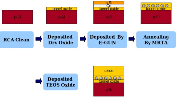
(31) 2.2 Experimental procedures. 2.2.1 The Oxidation of the Dry Oxide/Cobalt/amorphous Silicon Structure. There are five steps must be done in proper sequence. The first step, single-crystal 6 inch (100) oriented p-type silicon was cleaned with standard RCA recipes. The standard RCA clean process was immersed in the HCl bench at 120℃ for 10 minutes (called SCΙ process). Next, the wafers were cleaned with NH4OH at 120℃ for 10 minutes (called SCⅡ process) <2.1>. The last was dipped in HF a few seconds <2.2>. Second, the wafer was followed by dry oxidation in the atmospheric pressure chemical vapor deposition (APCVD) furnace to form 4.5nm-thick dry SiO2 layer as tunneling oxide <2.3>. Third, after the growth of tunnel oxide, a thin cobalt film and an amorphous silicon film were deposited in proper order on the tunneling oxide layer at the same run by Dual E-Gun Evaporation System (E-Gun). In this procedure, first the Co layer was deposited on the tunneling oxide layer, and then the a-Si layer was covered immediately. The deposition rate of the E-Gun was relied on adjustment of the current magnitude by a remote control. Not the rate magnitude but the current magnitude must be more exact because of the deposition thickness of cobalt film was the critical process to determine the size of the nanocrystals and the memory effect <2.4>. The cobalt film thickness was deposited about 10Å with deposition rate 0.1Å/sec and operation current range in 50-70uA, the a-Si film thickness was deposited about 200Å with deposition rate 0.2 Å/sec and operation current range in 70-80uA. The fourth step is the thermal treatment, the furnace oxidation processes at. 17.
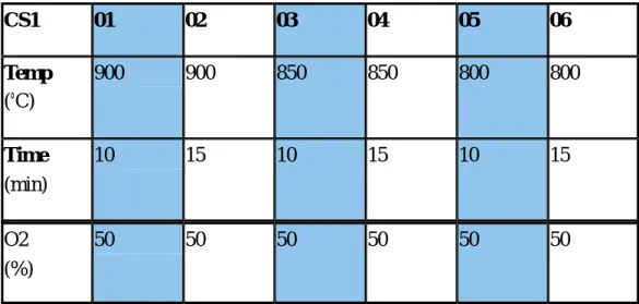
(32) different temperatures and times in the O2 surrounding (50%) <2.5>. The conditions of experimental parameters we set up are shown in Table 2.2.1. The cobalt thin film and the amorphous silicon became to the cobalt-silicide (CoSi2) and silicon dioxide at the same time after thermal oxidation, respectively. In the initial stage of the oxidation, the cobalt would react with little amorphous silicon to become cobalt-silicide, CoSi2, and then tended to form cobalt-silicide nanocrystals according to previous research. After this step, the micro-structure of sample was analyzed by Transmission Electron Microscope (TEM). The TEM figures can be more powerful evidence to confirm the shape of the nanocrystals. Finally, step five, the Al electrode 5000Å was patterned and coated by thermal evaporation coater. The complete experimental procedure for cobalt-silicide nanocrystals is shown in Figure 2.2.1. Subsequently, this metal insulator semiconductor (MIS) structure with CoSi2 nanocrystals embedded in dioxide was fabricated, and has prepared for electrical analyses. The Capacitance-Voltage measurement was analyzed the memory effect of the nanocrystal memories by HP4284A Precision LCR Meter.. 2.2.2 The Oxidation of the Dry Oxide/Cobalt/amorphous Silicon/Silicon Dioxide/amorphous Silicon Structure. There are six steps must be done in proper sequence. The first step, single-crystal 6 inch (100) oriented p-type silicon was cleaned with standard RCA recipes. The standard RCA clean process was immersed in the HCl bench at 120℃ for 10 minutes (called SCΙ process). Next, the wafers were cleaned with NH4OH at 120℃ for 10. 18.
(33) minutes (called SCⅡ process). The last was dipped in HF a few seconds. Second, the wafer was followed by dry oxidation in the atmospheric pressure chemical vapor deposition (APCVD) furnace to form 4.5nm-thick dry SiO2 layer as tunneling oxide. Third, after the growth of tunnel oxide, a thin cobalt film and an amorphous silicon film were deposited in proper order on the tunneling oxide layer at the same run by Dual E-Gun Evaporation System (E-Gun). In this procedure, first the cobalt layer was deposited on the tunneling oxide layer, and then the amorphous silicon layer was covered immediately. The deposition rate of the E-Gun was relied on adjustment of the current magnitude by a remote control. Not the rate magnitude but the current magnitude must be more exact because of the deposition thickness of cobalt film was the critical process to determine the size of the nanocrystals and the memory effect. The CoSi2 components were formed 1:2 ratio as Co to a-Si so the thickness of a-Si layer was double of Co layer. The cobalt film thickness was deposited about 10Å with deposition rate 0.1Å/sec and operation current range in 50-70uA, the a-Si film thickness was deposited about 20Å with deposition rate 0.1 Å/sec and operation current range in 70-80uA. Fourth, after the deposition of the Co/a-Si layers, once again a thin silicon-dioxide film and an amorphous silicon film were deposited in proper order on the tunneling oxide layer at the same run by Dual E-Gun Evaporation System (E-Gun). In this procedure, first the SiO2 layer was deposited on the lower a-Si layers, and then the a-Si layer was covered on top immediately. The action of this thin SiO2 layer was resisted the diffusion effect of cobalt silicide. The silicon-dioxide film thickness was deposited about 15Å with deposition rate 0.1Å/sec and operation current range in 50-60uA, the a-Si film thickness was deposited about 220Å with deposition rate 0.2 Å/sec and operation current range in 70-80uA. Step five is the thermal treatment, the furnace oxidation processes at different temperatures and times in the O2 surrounding (50%). There are many conditions we set up are shown in Table 19.
(34) 2.2.2. The stacked structure was oxidized to form cobalt-silicide (CoSi2) nanocrystals precipitated and embedded in dioxide, and the other a-Si become SiO2 at the same time. In the initial stage of the oxidation, the cobalt would react with the lower amorphous silicon to become cobalt-silicide, CoSi2, and then tended to form cobalt-silicide nanocrystals according to previous research. After this step, the micro-structure of sample was analyzed by Transmission Electron Microscope (TEM). The TEM figures can be more powerful evidence to confirm the shape of the nanocrystals. Finally, step six, the Al electrode 5000Å was patterned and coated by thermal evaporation coater. The complete experimental procedure for cobalt-silicide nanocrystals is shown in Figure 2.2.2. Subsequently, this metal insulator semiconductor (MIS) structure with CoSi2 nanocrystals embedded in dioxide was fabricated, and has prepared for electrical analyses. The Capacitance-Voltage measurement was analyzed the memory effect of the nanocrystal memories by HP4284A Precision LCR Meter.. 2.2.3 The Oxidation of the Dry Oxide/Cobalt/amorphous Silicon/TEOS Oxide Structure. There are six steps must be done in proper sequence. The first step, single-crystal 6 inch (100) oriented p-type silicon was cleaned with standard RCA recipes. The standard RCA clean process was immersed in the HCl bench at 120℃ for 10 minutes (called SCΙ process). Next, the wafers were cleaned with NH4OH at 120℃ for 10 minutes (called SCⅡ process). The last was dipped in HF a few seconds. Second, the 20.
(35) wafer was followed by dry oxidation in the atmospheric pressure chemical vapor deposition (APCVD) furnace to form 4.5nm-thick dry SiO2 layer as tunneling oxide. Third, after the growth of tunnel oxide, a thin cobalt film and an amorphous silicon film were deposited in proper order on the tunneling oxide layer at the same run by Dual E-Gun Evaporation System (E-Gun). In this procedure, first the Co layer was deposited on the tunneling oxide layer, and then the a-Si layer was covered immediately. The deposition rate of the E-Gun was relied on adjustment of the current magnitude by a remote control. Not the rate magnitude but the current magnitude must be more exact because of the deposition thickness of cobalt film was the critical process to determine the size of the nanocrystals and the memory effect. The CoSi2 components were formed 1:2 ratio as Co to a-Si so the thickness of a-Si layer was double of Co layer. The cobalt film thickness was deposited about 8Å with deposition rate 0.1Å/sec and operation current range in 50-70uA, the a-Si film thickness was deposited about 15Å with deposition rate 0.1 Å/sec and operation current range in 70-80uA. The fourth step is the thermal treatment, a metal rapid thermal annealing (Metal - RTA) in N2 ambient was performed to form the CoSi2 nanocrystals <2.6>. The cobalt thin film and the amorphous silicon became to the cobalt-silicide (CoSi2) only but not formed silicon dioxide. That is the reason we chose the ratio (1:2) as Co to a-Si. Therefore, the N2 Metal - RTA process transformed the Co layer and a-Si thin film layer to the CoSi2 spherical nanocrystals. The conditions of experimental parameters we set up are shown in Table 2.2.3. Fifth, the TEOS oxide 400Å was deposited on the CoSi2 nanocrystals by PECVD with reactant gases of TEOS flow 10 sccm mixed in Hydrogen plasma at 300℃ <2.7>. This step also was the critical process because it was related to retention and endurance characteristics. After this step, the micro-structure of sample was analyzed by Transmission Electron Microscope (TEM). The TEM figures can be more powerful evidence to confirm the 21.
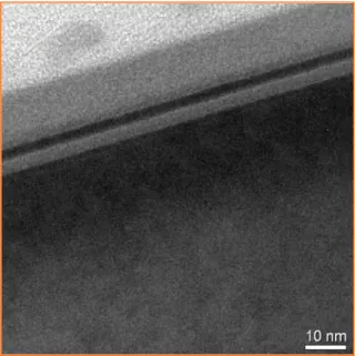
(36) shape of the nanocrystals. Finally, step six, the Al electrode 5000Å was patterned and coated by thermal evaporation coater. The complete experimental procedure for cobalt nanocrystals is shown in Figure 2.2.3. Subsequently, this metal insulator semiconductor (MIS) structure with CoSi2 nanocrystals embedded in dioxide was fabricated, and has prepared for electrical analyses. The Capacitance-Voltage measurement was analyzed the memory effect of the nanocrystal memories by HP4284A Precision LCR Meter.. 2.3 Results and discussions. 2.3.1 The Material Characteristic and Electrical Characteristics of the Dry Oxide/Cobalt/amorphous Silicon Structure Figure 2.3.1-1(a) and Figure 2.3.1-1(b) represents typical bright-field, cross-section TEM images. Figure 2.3.1-1(a) shows the standard structure before oxidation. We can see the structure, the cobalt layer and a-Si layer were continuous above the tunnel oxide. In Figure 2.3.1-1(b), a sample after 900℃ dry oxidation is shown. The separated cobalt-silicide nanocrystals were found to distribute in the control oxide randomly. It is found that the cobalt-silicide nanocrystals had diffusion phenomenon in both the tunnel oxide and control oxide. The distribution of cobalt-silicide nanocrystals is closer to top, it means that the diffusion phenomenon in control oxide is more serious than tunnel oxide, because the quality of tunnel oxide layer formed with dry oxidation in the atmospheric pressure chemical vapor deposition furnace is better. The variation in morphology of these samples with 22.
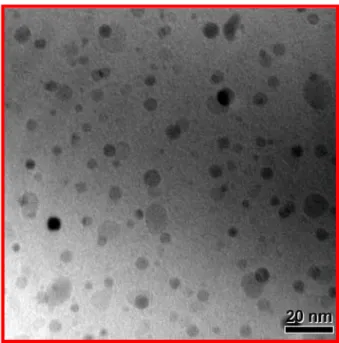
(37) different oxidation temperatures is related to the rate of silicide formation. As the a-Si film was oxidized, oxygen may diffuse to the oxide/Si interface to form silicon oxide. If the CoSi2 nanocrystals were already formed, they may move farther away from the oxide/Si interface. As a result, the selection of oxidation temperature and time are critical for forming nanocrystals. In growing SiO2 film from Si, a film of SiO2 with a thickness of x0 consumes a layer of crystalline Si _c-Si_ about 0.45x0. Therefore, a Si substrate about 3.2 nm thick was oxidized to contribute to about a 7 nm thick SiO2 in addition to the 3 nm thick tunnel oxide. The electrical characteristics as illustrated in Figure 2.3.1-2(a). Figure 2.3.1-2(b). Figure 2.3.1-2(c) and Figure 2.3.1-2(d) are the capacitance-voltage (C-V) measurement of the samples dry oxidized at 900℃. 850℃ and 800℃, respectively. The capacitance-voltage characteristics of those three conditions are rather poor, there is almost no hysteresis in those three figures. This reason is considered that the diffusion effect of cobalt-silicide in oxide layer, as shown in Figure 2.3.1-1(b). The cobalt-silicide nanocrystals diffused close to the top, and easily produced some fatal discharge paths, cause electrons cannot maintain stored in the cobalt-silicide nanocrystals.. 2.3.2 The Material Characteristic and Electrical Characteristics of the Dry Oxide/Cobalt/amorphous Silicon/Silicon Dioxide/amorphous Silicon Structure. Figure 2.3.2-1 represents typical bright-field, cross-section TEM images of the sample after 800℃ dry oxidation. As seen in this figure, the well-separated and spherical cobalt-silicide nanocrystals embedded in the silicon dioxide layer were clearly observed. It worthily notices that the diffusion effect of cobalt-silicide 23.
(38) nanocrystals of the dry oxide/cobalt/amorphous silicon/silicon dioxide/amorphous silicon structure was not so serious in the tunnel oxide and still above the tunnel oxide. It implies the diffusion phenomenon was restrained successfully by the silicon dioxide layer between those two amorphous silicon layers. The lower amorphous silicon layer reacted with cobalt to formed cobalt-silicide, and the top amorphous silicon layer was completely oxidized to server as the control oxide layer. The characteristic is beneficial for the reliability and the yield of the memory device. Furthermore, Figure 2.3.2-2(a) shows the plan-view TEM image of a sample after 800 °C oxidation. The mean size and aerial density of the cobalt-silicide nanocrystals were measured to be about 4.42nm and 2.3°1011/cm2, respectively. The size distribution of the nanocrystals is shown in Figure 2.3.2-2(b). The electrical characteristics as illustrated in Figure 2.3.2-3(a) and Figure 2.3.2-3(b) are the capacitance-voltage (C-V) measurement of the samples dry oxidized at 800℃. It implies the forward and reverse voltage sweep C-V characteristics, indicating the electron charging and discharging effects of the CoSi2 nanocrystals embedded in SiO2. The bidirectional C-V sweeps were performed from deep inversion to deep accumulation and in reverse, which exhibited an electron charging effect. When the voltage swept from (+6) to (-6) V and back to (+6) V at the same point, a significant threshold voltage shift of 1V is observed. As the “program” voltage decreased to 3V, a visible threshold voltage shift about 0.8V is observed, too. The goal of capacitance -voltage measurement is to confirm whether there are some traps or nanocrystals in the MOS structure as charge storage. It is perceived that both of the hysteresis is counterclockwise, which is due to injection of electrons from the deep inversion layer and injection of holes from the deep accumulation layer of silicon substrate [2.3]. The result of the C-V shift indicates that the charging effects of CoSi2 nanocrystals are more significant than those of the semiconductor nanocrystals. 24.
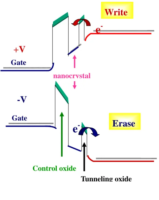
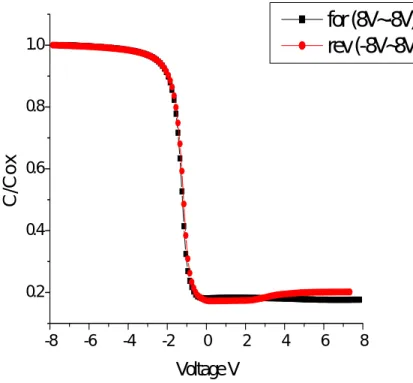
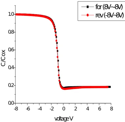
(39) Figure 2.3.2-4 shows the band diagrams of “write” and “erase” operations with different gate polarities of the memory device. When the device is written or programmed, the electrons directly tunnel from the silicon substrate through the tunnel oxide, and are trapped in the CoSi2 nanocrystals. On the other hand, when the device is erased, the electrons may tunnel back to the deep accumulation layer of silicon substrate. The control oxide is utilized to prevent the carriers of gate electrode injecting into the CoSi2 nanocrystals by Fowler-Nordheim (F-N) tunneling. The most important advantage using the metal nanocrystals over their semiconductor counterparts is that the metal nanocrystals do not bear a voltage drop from gate voltage, which means all the voltages provided from control gate are dropped to tunnel oxide and control oxide. The operating voltage of the memory devices with conventional floating gate or semiconductor nanocrystals embedded in SiO2 is above 7 or 5 V. In our approach to fabricate the CoSi2 nanocrystals embedded in SiO2 by dry oxidation 800°C, a lower programming voltage of 3V realizes a significant threshold voltage shift of 0.8V. The voltage is sufficient to be defined as “1” and “0” by a typical sensing amplifier for a memory device.. 2.3.3 The Electrical Characteristics of the Dry Oxide/Cobalt/amorphous Silicon/TEOS Oxide Structure. The electrical characteristics as illustrated in Figure 2.3.3-1(a) and Figure 2.3.3-1(b) are the capacitance-voltage (C-V) measurement of the samples annealing at 800℃ 100 seconds. It implies the forward and reverse voltage sweep C-V characteristics, indicating the electron charging and discharging effects of the CoSi2 nanocrystals 25.
(40) embedded in SiO2. The bidirectional C-V sweeps were performed from deep inversion to deep accumulation and in reverse, which exhibited an electron charging effect. A pronounced capacitance-voltage hysteresis is observed with a memory window of 2.2V under the 8V programming voltage, and 4V under the 10V programming voltage, but the hysteresis are imperfect distinctly. This might be the quality of the PECVD TEOS oxide layer was not good enough. This deficiency would make to some defects and fixed charges in the oxide layer, cause the capacitance -voltage hysteresis shift to negative.. 2.4 Summary. From above-mentioned experiment, it is found that the cobalt-silicide nanocrystals had diffusion phenomenon in both the tunnel oxide and control oxide in the Dry Oxide/Cobalt/Amorphous Silicon structure, and it is more serious that the diffusion phenomenon in control oxide than tunnel oxide, because the quality of tunnel oxide layer formed with dry oxidation in the atmospheric pressure chemical vapor deposition furnace is better. The diffusion phenomenon caused the capacitance -voltage characteristics of those three conditions are rather poor, even no hysteresis. So we suggested the Dry Oxide/Cobalt/amorphous Silicon/Silicon Dioxide/ Amorphous Silicon structure. It is founded that diffusion phenomenon was restrained successfully by the silicon dioxide layer between those two amorphous silicon layers. In all experimental conditions, it shows that oxidation at 800℃ for ten minutes has better characteristic according to the observable C-V shift. As seen in this TEM image,. 26.
(41) the well-separated and spherical cobalt-silicide nanocrystals embedded in the silicon dioxide layer were clearly observed. In addition, CoSi2 nanocrystals do not bear a voltage drop from gate voltage, which means all the voltages provides from control gate are dropped to tunnel oxide and control oxide, and obtain profit over other semiconductor counterparts. In conventional floating gate nonvolatile memory devices, the operating voltage is above 7 V which is not easy to scale down due to the thick gate-stacked structure. In our approach to growth the CoSi2 nanocrystals embedded in SiO2, a lower programming voltage of 3V actualize a significant threshold voltage shift, 0.8V, which is sufficient to be defined as “1” and “0” by a typical sense amplifier for a memory device. The third method, the Dry Oxide/ Cobalt/amorphous Silicon/TEOS Oxide structure, was suggested to avoid the diffusion phenomenon of cobalt silicide. A pronounced capacitance-voltage hysteresis was observed, but the hysteresis was imperfect distinctly. This might be the quality of the PECVD TEOS oxide layer was not good enough. This deficiency would make to some defects and fixed charges in the oxide layer, cause the capacitance -voltage hysteresis shift to negative.. 27.
(42) Chapter 3. A Novel Approach of Fabricating Cobalt Nanocrystals for Nonvolatile Memory Application. 3.1 Introduction. Demand to a high density and high performance nonvolatile memory has rapidly grown as the market for mobile information device has expanded. And flash memory is the most widely used nonvolatile memory because high density, low cost, stable operation and so on. The major advantages of metal nanocrystals over their semiconductor counterparts include (1) higher density of states around the Fermi level, (2) stronger coupling with the conduction channel, (3) a wide range of available work functions, (4) smaller energy perturbation due to carrier confinement [3.1], and (5) the nanocrystals do not bear a voltage drop from gate voltage, which means all the voltages provided from control gate are dropped to tunnel oxide and control oxide and gains advantage. For metal nanocrystals memory device, the select of work function creates a deeper potential well to enhance retention time without sacrificing injection efficiency. And traps are screened out due to the large density of states in metal. As the result of these advantages, we can select various metals which have high work function to manufacture our metal nanocrystals. One of the methods that manufacture metal nanocrystals is self-assembled metal dot by means of thermal annealing. To form the 28.
(43) self-assembled metal nanocrystals as floating gate, it could deposit a wetting layer of metal by evaporating or sputtering. And then the sample to deal with a thermal process, it is obviously to create nanocrystals dot as Figure 3.1-1. This phenomenon could explain that undulation of dot patterns is the result of energy minimization among the surface and elastic energies and various long-rang force [3.2]. Nanocrystals in a more regular pattern and with minimal separation can be obtained. And the other hand, the film is annealed at elevated temperature close to its eutectic temperature with the substrate in the ambient to transfer the wetting layer into nanocrystals. This process is achieved through the relation of film stress and limited by the surface mobility. Some long-range forces such as the dispersion force and the electrical double layers will also affect the nanocrystals size and location distributions [3.3]. In this chapter, we demonstrated nanocrystals formation of the cobalt which has a wide work function and showed the memory window of metal nonvolatile memory (MVM). In this experiment, we proposed a cobalt (Co) nanocrystal memory device. The material about Co was suitable for the MOSFET devices as the devices scaling down. Then we studied on the memory characteristics of the metal nanocrystal. A significant threshold-voltage shift due to the charge trapping in the Co dots is observed.. 3.2 Experimental procedures. 3.2.1 The Annealing of the Dry Oxide/Cobalt/ TEOS Oxide Structure. There are six steps must be done in proper sequence. The first step, single-crystal 6. 29.
(44) inch (100) oriented p-type silicon was cleaned with standard RCA recipes. The standard RCA clean process was immersed in the HCl bench at 120℃ for 10 minutes (called SCΙ process). Next, the wafers were cleaned with NH4OH at 120℃ for 10 minutes (called SCⅡ process) <2.1>. The last was dipped in HF a few seconds <2.2>. Second, the wafer was followed by dry oxidation in the atmospheric pressure chemical vapor deposition (APCVD) furnace to form 4.5nm-thick dry SiO2 layer as tunneling oxide <2.3>. Third, after the growth of tunnel oxide, a thin cobalt film was deposited on the tunneling oxide layer by Dual Electron-Gun Evaporation System (E-Gun). The deposition rate of the E-Gun was relied on adjustment of the current magnitude by a remote control. Not the rate magnitude but the current magnitude must be more exact because of the deposition thickness of cobalt film was the critical process to determine the size of the nanocrystals and the memory effect <2.4>. The cobalt film thickness was deposited about 10Å with deposition rate 0.1Å/sec and operation current range in 50-70uA. The fourth step is the thermal treatment, rapid thermal annealing (RTA) in N2 ambient was performed to form the Co nanocrystals <2.6>. The method mainly utilizes the difference of Gibbs free energies of materials at various temperatures. At the high temperatures, the material will be changed itself components to reduce the free energy for steadily. The reason of the Co film turn to the Co nanocrystals was due to the strong cohesion of the material. When the thin film was in thermal annealing, the surface energy would be reduced by increasing the surface area. Therefore, the N2 Metal - RTA process transformed the Co thin film layer to the Co spherical nanocrystals. This mechanism is called “self-assembled” as Figure 3.1-1. The conditions that we set up are shown in Table 3.2.1. Next, step five, the TEOS oxide 400Å was deposited on the Co nanocrystals by Plasma Enhanced Chemical Vapor Deposition (PECVD) with reactant gases of TEOS flow 10 sccm mixed in Hydrogen plasma at 300℃ <2.7>. This step was the critical process because 30.
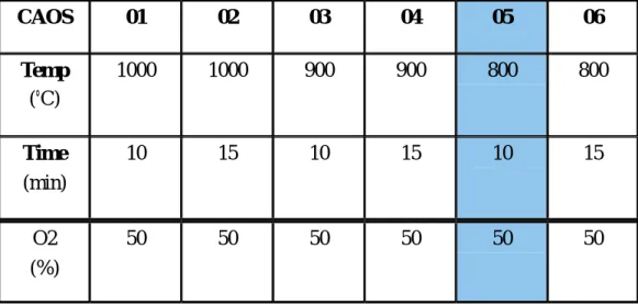
(45) it was related to retention and endurance characteristics. After this step, the micro-structure of this sample was analyzed by Transmission Electron Microscope (TEM). The TEM figures can be more powerful evidence to confirm the shape of the nanocrystals. Finally, step six, the Al electrode 5000Å was patterned and coated by thermal evaporation coater. The complete experimental procedure for cobalt nanocrystals is shown in Figure 3.2.1. Subsequently, this metal insulator semiconductor (MIS) structure with Co nanocrystals embedded in dioxide was fabricated, and has prepared for electrical analyses. The Capacitance-Voltage measurement was analyzed the memory effect of the nanocrystal memories by HP4284A Precision LCR Meter.. 3.2.2 The Oxidation of the Dry Oxide/Cobalt/ TEOS Oxide Structure. There are six steps must be done in proper sequence. The first step, single-crystal 6 inch (100) oriented p-type silicon was cleaned with standard RCA recipes. The standard RCA clean process was immersed in the HCl bench at 120℃ for 10 minutes (called SCΙ process). Next, the wafers were cleaned with NH4OH at 120℃ for 10 minutes (called SCⅡ process). The last was dipped in HF a few seconds. Second, the wafer was followed by dry oxidation in the atmospheric pressure chemical vapor deposition (APCVD) furnace to form 4.5nm-thick dry SiO2 layer as tunneling oxide. Third, after the growth of tunnel oxide, a thin cobalt film was deposited on the tunneling oxide layer by Dual Electron-Gun Evaporation System (E-Gun). The deposition rate of the E-Gun was relied on adjustment of the current magnitude by a. 31.
(46) remote control. Not the rate magnitude but the current magnitude must be more exact because of the deposition thickness of cobalt film was the critical process to determine the size of the nanocrystals and the memory effect. The cobalt film thickness was deposited about 10Å with deposition rate 0.1Å/sec and operation current range in 50-70uA. Next, step four, the TEOS oxide 400Å was deposited on the Co thin film by Plasma Enhanced Chemical Vapor Deposition (PECVD) with reactant gases of TEOS flow 10 sccm mixed in Hydrogen plasma at 300℃. This step was the critical process because it was related to retention and endurance characteristics. The fifth step is the thermal treatment, the furnace oxidation processes at different temperatures and times in the O2 surrounding (50%) <2.5>. The conditions of experimental parameters we set up are shown in Table 3.2.2. The cobalt thin film became to the cobalt nanocrystals after thermal oxidation, and the oxide layer deposited by PECVD would be oxidized again to improve the quality at the same time. After this step, the micro-structure of sample was analyzed by Transmission Electron Microscope (TEM). The TEM figures can be more powerful evidence to confirm the shape of the nanocrystals. Finally, step six, the Al electrode 5000Å was patterned and coated by thermal evaporation coater. The complete experimental procedure for cobalt nanocrystals is shown in Figure 3.2.2. Subsequently, this metal insulator semiconductor (MIS) structure with Co nanocrystals embedded in dioxide was fabricated, and has prepared for electrical analyses. The Capacitance-Voltage measurement was analyzed the memory effect of the nanocrystal memories by HP4284A Precision LCR Meter.. 32.
數據

+7
相關文件
From the findings reported above, it is undeniable that there has been huge progress in ITEd in Hong Kong schools, as reflected by the significantly improved infrastructure, the
• helps teachers collect learning evidence to provide timely feedback & refine teaching strategies.. AaL • engages students in reflecting on & monitoring their progress
Robinson Crusoe is an Englishman from the 1) t_______ of York in the seventeenth century, the youngest son of a merchant of German origin. This trip is financially successful,
fostering independent application of reading strategies Strategy 7: Provide opportunities for students to track, reflect on, and share their learning progress (destination). •
Strategy 3: Offer descriptive feedback during the learning process (enabling strategy). Where the
How does drama help to develop English language skills.. In Forms 2-6, students develop their self-expression by participating in a wide range of activities
double-slit experiment is a phenomenon which is impossible, absolutely impossible to explain in any classical way, and.. which has in it the heart of quantum mechanics -
using tungsten single crystal emitters the thermally-assisted Schottky type, using emitters of zirconium oxide. field emission
