國立高雄大學應用物理學系研究所
碩士論文
在
p
層和藍寶石基板上使用多層石墨烯透明電極的氮化銦
鎵/氮化鎵多重量子井發光二極體中增強元件性能和載子
傳輸
Enhancement of device performance and carrier transport in
InGaN/GaN multiple-quantum well light emitting diodes with
multilayer graphene transparent electrodes on the p-layer and on the
sapphire substrate.
研究生:王盈翔 撰
指導教授:馮世維 博士
致謝
碩士班兩年的生涯中要感謝許多幫助我的貴人,才能讓我順利的完成學業,首先要 感謝的是我的父母與妹妹,感謝他們為家庭默默付出,使我可以專心在學業上,感謝他 們給予我經濟上與精神上的幫助與鼓勵,讓我在求學過程中遇到困難也能夠有信心的去 面對。再來是感謝我的指導教授馮世維博士,馮老師在我研讀碩士班過程中不時地給予 我建議與指導,使我學習到解決問題的能力,在實驗與論文撰寫方面也給予很多建議與 指導,對於研究上的熱誠以及處事細心認真的態度實在值得我們學習;在研究過程中還 要感謝蔡進譯博士,在論文撰寫方面也給予很多建議與指導,同時也要感謝中正大學光 機電整合工程研究所王祥辰博士,在 PL 量測方面的協助。接者,要感謝的就是陳建勳 博士與賴志明博士,在我口試上提出在研究上有所不足的地方,給予我許多的意見及幫 助。最後,要感謝昱翔學長、保勛學長、千娪學姊,協助我在研究上所遇到的問題,以 及研究所同學偉銘、博勛、俊毅、威佐、瓊毅,在碩士生活中互相幫助與分憂,讓我的 求學生活更加充實與快樂;也感謝少強學弟,平時幫我分擔雜事,使我能夠順利完成碩 士求學生涯,在此獻上我最誠摯的感激與祝福。 王盈翔 敬上 2018/07I
在p層和藍寶石基板上使用多層石墨烯透明電極的氮化銦鎵/氮化
鎵多重量子井發光二極體中增強元件性能和載子傳輸
指導教授:馮世維 博士 國立高雄大學應用物理學研究所 學生:王盈翔 國立高雄大學應用物理學研究所 摘要 在第一章,我們呈現使用多層石墨烯透明電極的氮化銦鎵/氮化鎵多重量子井發光 二極體的光學顯微圖像(Optical microscopy images)、電激螢光圖像(EL images)、電激螢 光(EL)、電流-電壓(I-V)、以及時間解析電激螢光(TREL)實驗結果。在氮化鎵發光二極 體的p層使用石墨烯作為透明導電電極,極大增強光學和電學性能。在p層具有石墨烯透 明導電電極的氮化鎵發光二極體的電激螢光強度、電流密度、輸出功率、和外部量子效 率可以分別提高18%、10%、26%、和15%。在時間解析電激螢光測量中,具有石墨烯 透明導電電極的氮化鎵發光二極體的較短響應時間、上升、和延遲時間提供更有效的載 子注入、傳輸、和鬆弛。在p層具有多層石墨烯透明電極的發光二極體具有更多的載子 注入,需要更多的時間用於載子復合因而顯示更長的複合時間。另一方面,在氮化鎵發 光二極體中的藍寶石基板鍍石墨烯,也可增強光學和電學性能。在藍寶石基板鍍石墨 烯,氮化鎵發光二極體的電致發光強度、電流密度、輸出功率、和外部量子效率可以分 別提高12%、10%、12%、和12%。氮化鎵發光二極體的較短響應、上升、和延遲時間 提供更有效的載子注入、傳輸、和鬆弛。因為有更多的載子注入,需要更多的時間用於II 載子復合,因此顯示更長的複合時間。 在第二章,我們呈現使用多層石墨烯透明電極的氮化銦鎵/氮化鎵量子井磊晶層與 發光二極體的電子顯微鏡(SEM)、陰極發光(CL)、原子力顯微鏡(AFM)、X光繞射分析 (XRD)、光激螢光(PL)、時間解析光激螢光(TRPL)、電激螢光圖像(EL images)、電激螢 光(EL)、電流-電壓(I-V)、以及時間解析電激螢光(TREL)的實驗結果。在氮化銦鎵/氮化 鎵多重量子井磊晶層的p層使用石墨烯作為透明導電電極,大幅增強光學和材料特性。 具有石墨烯透明導電電極的氮化銦鎵/氮化鎵多重量子井磊晶層顯示出更大的表面粗糙 度、較強的銦聚集、和更強的光激螢光強度。在時間解析光激螢光測量中,具有石墨烯 的氮化銦鎵/氮化鎵多重量子井磊晶層的較短衰減時間與增強銦聚集一致。在氮化銦鎵/ 氮化鎵多重量子井發光二極體的p層使用石墨烯作為透明導電電極,大幅增強光學和電 學性能,可以增強電激螢光強度、電流密度、輸出功率、和外部量子效率。在時間解析 電激螢光測量中,具有石墨烯透明導電電極的氮化鎵基發光二極體的較短響應、上升、 和延遲時間提供更有效的載子注入、傳輸、和鬆弛。因為有更多的載子注入,需要更多 的時間用於載子復合,因此顯示更長的複合時間。 關鍵字:氮化銦鎵/氮化鎵量子井發光二極體;多層石墨烯透明電極;時間解析電激螢光; 載子傳輸;響應時間
III
Enhancement of device performance and carrier transport in
InGaN/GaN multiple-quantum well light emitting diodes with
multilayer graphene transparent electrodes on the p-layer and on
the sapphire substrate
Advisor: Dr. Shih-Wei Feng Department of Applied Physics National University of Kaohsiung
Student: Ying-Hsiang Wang Department of Applied Physics National University of Kaohsiung
ABSTRACT
In the first chapter, we have shown the experimental results of optical microscopy images, EL images, EL spectrum, current density, and TREL measurements of the multilayer graphene transparent electrodes InGaN/GaN MQW LEDs. The optical and electrical performances were greatly enhanced by employing graphene as transparent conductive electrodes on the p-layer of GaN-based LEDs. The EL intensity, current density, output power, and EQE of the GaN-based LEDs with a graphene transparent conductive electrode on the
p-layer can be enhanced as high as 18, 10, 26, and 15 % of those without a graphene
transparent conductive electrode, respectively. In TREL measurement, the shorter response, rise, and delay times of the GaN-based LEDs with a graphene transparent conductive
IV
electrode provide more efficient carrier injection, transport, and relaxation. The LEDs with multilayer graphene transparent electrodes on the p-layer have more carrier injection, so the LEDs need more time for carrier recombination and show a longer recombination time. On the other hand, the optical and electrical performances were also enhanced by employing graphene as transparent conductive electrodes on the sapphire substrate in GaN-based LEDs. The EL intensity, current density, output power, and EQE of the GaN-based LEDs with a graphene transparent conductive electrode on the sapphire substrate can be enhanced as high as 12, 10, 12, and 12 % of those without a graphene transparent conductive electrode, respectively. The shorter response, rise, and delay times of the GaN-based LEDs with a graphene transparent conductive electrode provide more efficient carrier injection, transport, and relaxation. The GaN-based LEDs with multilayer graphene transparent electrodes on the sapphire substrate have more carrier injection, so the GaN-based LEDs need more time for carrier recombination and show a longer recombination time.
In the second chapter, we have shown the experimental results of SEM, CL, XRD, AFM, PL, TRPL, EL images EL spectrum, current density, and TREL measurements of the InGaN/GaN MQW epilayers and LEDs with graphene as transparent conductive electrodes. The optical and material characteristics were greatly enhanced by employing graphene as transparent conductive electrodes on the p-layer of InGaN/GaN MQW epilayers. InGaN/GaN MQW epilayers with graphene transparent conductive electrodes show a larger surface roughness, enhanced indium aggregation, and stronger PL intensity. In TRPL measurement, the shorter decay times of the InGaN/GaN MQW epilayers with graphene are consistent with an enhanced indium aggregation. The optical and electrical performances were greatly enhanced by employing graphene as transparent conductive electrodes on the p-layer of InGaN/GaN MQW LEDs. The EL intensity, current density, output power, and EQE of the InGaN/GaN MQW LEDs with a graphene transparent conductive electrode on the p-layer can be enhanced. In TREL measurement, the shorter response, rise, and delay times of the
V
GaN-based LEDs with a graphene transparent conductive electrode provide more efficient carrier injection, transport, and relaxation. The LEDs with multilayer graphene transparent electrodes on the p-layer have more carrier injection, so the LEDs need more time for carrier recombination and show a longer recombination time.
Keywords: InGaN/GaN MQW LEDs;Multilayer graphene transparent electrodes;
VI
Contents
中文摘要
……….………I
Abstract………...III
Contents………...VI
Figure Captions………
....VIII
Chapter 1 Enhancement of device performance and carrier transport in
InGaN/GaN multiple-quantum well light emitting diodes with multilayer
graphene transparent electrodes on the p-layer and on the sapphire
substrate...1
1.1 Introductions...………..1
1.2 Motivation.……….………...…...3
1.3 Device characteristics and carrier transport properties of InGaN/GaN MQW LEDs without and with multilayer graphene transparent electrodes on the p-layer ..……...…...4
1.3.1 Investigation procedures and sample preparation..………..………...4
1.3.2 Optical microscope images study………...4
1.3.3 EL images and EL spectra studies...5
1.3.4 Current density, output power, and EQE studies………...6
1.3.5 Time-resolved Electroluminescence (TREL) Study………...7
1.4 Device characteristics and carrier transport properties of InGaN/GaN MQW LEDs without and with multilayer graphene transparent electrodes on the sapphire substrate....8
1.4.1 Investigation procedures and sample preparation………..8
1.4.2 Optical microscope images study………...9
1.4.3 EL images and EL spectra studies………...10
1.4.4 Current density, output power, and EQE studies....…...………...10
VII
1.5 Discussion and summary...12
References...15
Chapter
2
Efficient
recombination
dynamics
in
InGaN/GaN
multiple-quantum-wells and efficient device performance and carrier
transport in InGaN/GaN LEDs by using multilayer graphene transparent
electrodes….………..…36
2.1 Introduction.………...…....…..…..36
2.2 Motivation………….……….37
2.3 Sample preparations and investigation procedures ………….……….………….37
2.4 Optical and material characteristics of InGaN/GaN MQW epilayers without and with multilayer graphene transparent electrodes on the p-GaN layer……...………...38
2.4.1 Scanning electron microscope (SEM) and cathodoluminescence (CL)...38
2.4.2 Atomic force microscopy (AFM) and x-ray diffraction (XRD) studies……...39
2.4.3 Temperature-dependent photoluminescence (PL) and time-resolved photoluminescence (TRPL) studies………..39
2.5 Device characteristics and carrier transport properties of InGaN/GaN MQW LEDs without and with multilayer graphene transparent electrodes on the p-GaN layer……..40
2.5.1 EL images and EL spectra studies………..………….……….…....41
2.5.2 Current density, output power, and EQE studies…..………….……….…..41
2.5.3 Time-resolved electroluminescence (TREL) study……….……….42
2.6 Discussion and Summary...43
VIII
Figure Captions
Figure 1.1 The applications of graphene……….17 Figure 1.2 The quality and production cost of various kinds of graphene………..17 Figure 1.3 Schematic diagram of the G-VLED fabrication process………...18 Figure 1.4 (a) Light output vs. current for G-VLEDs and R-VLEDs. (b) EL image of G-VLEDs. (c) Current-voltage characteristics of G-VLEDs and R-VLEDs before annealing; (d) Leakage current of G-VLEDs and R-VLEDs before annealing……….18 Figure 1.5 (a) GaN-based UV-LED structures, and (b) fabricated device covered with GO nanosheets………19 Figure 1.6 (a) Light output power vs. current of conventional, l-GO-passivated, and h-GO-passivated UV-LEDs. (d)I-V cures of p-GaN with and without GO nanosheets measured by (e)vertical and (f)in-plane configuration. Higher (lower) current in vertical (in-plane) configuration was observed from p-GaN with GO compared to that without GO. Energy band diagram of p-GaN (g)without and (h)with h-GO. (i) Schematic energy band diagram of active region in UV-LED with applied forward bias……….…19 Figure 1.7 (a) UPS spectra of as-grown and doped graphene films around the secondary-electron cutoff region and the Fermi level position. (b)Energy band diagram at the graphene/p-GaN interface………20 Figure 1.8 Experimental flow chart of this chapter……….21 Figure 1.9 Fabrication processes of the InGaN/GaN LEDs with the graphene transparent conductive electrodes on the p-GaN layer:(a) Graphene was grown on a copper sheet by a chemical vapor deposition (CVD). (b) Poly(methyl methacrylate) (PMMA) was spin-coated on the graphene/copper sheet. (c) The copper sheet was etched in a 1 wt. % (NH4)2S2O8 solution (d) The graphene with PMMA was transferred onto the p-GaN layer of the InGaN/GaN LEDs. (e) The PMMA layer was removed by acetone solution………..22 Figure 1.10 Optical microscope images of the samples (a) LED1, (b) LED2, (c) LED3, (d)
IX
LED1Gp, (e) LED2Gp, and (f) LED3Gp………...22
Figure 1.11 EL images for the samples (1)~(6) LED1, (7)~(12) LED1Gp, (13)~(18) LED2, (19)~(24) LED2Gp, (25)~(30) LED3, and (31)~(36) LED3Gp with the excitations of 2.5, 2.6, 2.7, 2.8, 2.9, and 3.0 Volt electron voltages under room temperature, respectively…...…….23 Figure 1.12 Experimental setup of EL measurement………..23 Figure 1.13 EL spectra as a function of applied voltages for the samples (a) LED1, (b) LED2, (c) LED3, (d) LED1Gp, (e) LED2Gp, and (f) LED3Gp at room temperature………..24
Figure 1.14 EL peak position as a function of applied voltages for the samples LED1, LED2, LED3, LED1Gp, LED2Gp, and LED3Gp at room temperature………...24
Figure 1.15 Current density (I) vs. applied voltage (V) for the samples (a) LED1 and LED1Gp, (b) LED2 and LED2Gp, and (c) LED3 and LED3Gp………...25
Figure 1.16 Output power vs. applied voltage (V) for the samples (a) LED1 and LED1Gp, (b) LED2 and LED2Gp, and (c) LED3 and LED3Gp……….25
Figure 1.17 Output power vs. applied current (I) for the samples (a) LED1 and LED1Gp, (b) LED2 and LED2Gp, and (c) LED3 and LED3Gp……….26
Figure 1.18 External quantum efficiency (EQE) as functions of applied voltage (V) for the samples (a) LED1 and LED1Gp, (b) LED2 and LED2Gp, and (c) LED3 and LED3Gp……..26
Figure 1.19 Experimental setup of TREL measurement……….27 Figure 1.20 TREL profiles of the samples (a) LED1, (b) LED2, (c) LED3, (d) LED1Gp, (e) LED2Gp, and (f) LED3Gp at room temperature………..27
Figure 1.21 Response, rise, and delay times as a function of applied pulse voltage for the samples (a) LED1 and LED1Gp, (b) LED2 and LED2Gp, and (c) LED3 and LED3Gp……..28
Figure 1.22 Recombination time as a function of applied pulse voltage for the samples (a) LED1 and LED1Gp, (b) LED2 and LED2Gp, and (c) LED3 and LED3Gp……….28
Figure 1.23 Experimental flow chart of this chapter………..29 Figure 1.24 Fabrication processes of the InGaN/GaN LEDs with the graphene transparent
X
conductive electrodes on the sapphire substrate: (a) Graphene was grown on a copper sheet by a chemical vapor deposition (CVD). (b) Poly(methyl methacrylate) (PMMA) was spin-coated on the graphene/copper sheet. (c) The copper sheet was etched in a 1 wt. % (NH4)2S2O8 solution. (d) The graphene with PMMA was transferred onto the sapphire substrate of the InGaN/GaN LEDs. (e) The PMMA layer was removed by acetone solution……….30 Figure 1.25 Optical microscope images of the samples (a) LED1, (b) LED2, (c) LED3, (d) LED1Gs, (e) LED2Gs, and (f) LED3Gs………30
Figure 1.26 EL images for the samples (1)~(6) LED1, (7)~(12) LED1Gs, (13)~(18) LED2, (19)~(24) LED2Gs, (25)~(30) LED3, and (31)~(36) LED3Gs with the excitations of 2.5, 2.6, 2.7, 2.8, 2.9, and 3.0 Volt electron voltages under room temperature, respectively………....31 Figure 1.27 EL spectra as a function of applied voltages for the samples (a) LED1, (b) LED2, (c) LED3, (d) LED1Gs, (e) LED2Gs, and (f) LED3Gs at room temperature………...31
Figure 1.28 EL peak position as a function of applied voltages for the samples LED1, LED2, LED3, LED1Gs, LED2Gs, and LED3s at room temperature………32
Figure 1.29 Current density (I) vs. applied voltage (V) for the samples (a) LED1 and LED1Gs, (b) LED2 and LED2Gs, and (c) LED3 and LED3Gs………32
Figure 1.30 Output power vs. applied voltage (V) for the samples (a) LED1 and LED1Gs, (b) LED2 and LED2Gs, and (c) LED3 and LED3Gs……….…33
Figure 1.31 Output power vs. applied current (I) for the samples (a) LED1 and LED1Gs, (b) LED2 and LED2Gs, and (c) LED3 and LED3Gs……….33
Figure 1.32 External quantum efficiency (EQE) as functions of applied voltage (V) for the samples (a) LED1 and LED1Gs, (b) LED2 and LED2Gs, and (c) LED3 and LED3Gs……...34
Figure 1.33 TREL profiles of the samples (a) LED1, (b) LED2, (c) LED3, (d) LED1Gs, (e) LED2Gs, and (f) LED3Gs at room temperature………..34
XI
samples (a) LED1 and LED1Gs, (b) LED2 and LED2Gs, and (c) LED3 and LED3Gs……...35
Figure 1.35 Recombination time as a function of applied pulse voltage for the samples (a) LED1 and LED1Gs, (b) LED2 and LED2Gs, and (c) LED3 and LED3Gs………..35
Figure 2.1 (a) Multi-layer graphene was transferred onto the p-GaN layer; (b) applying an inductively coupled plasma (ICP) to etch the n-type GaN layer; (c)the p- and n-electrode were fabricated on the MLG layer and the n-type GaN layer, respectively; (d) structure of a MLG-GLED……….47 Figure 2.2 (a) Images of MLG-GLEDs. (b) I-V measurement. (c) Light intensity-I measurement. (d) comparison of GLED peak wavelength-I measurement with ITO electrodes, with, and without graphene electrodes ………....47 Figure 2.3 Experimental flow chart of this chapter……….48 Figure 2.4 Fabrication processes of the InGaN/GaN MQW LEDs with graphene transparent conductive electrodes on the p-GaN layer:(a) Graphene was grown on a copper sheet by a chemical vapor deposition (CVD). (b) Poly(methyl methacrylate) (PMMA) was spin-coated on the graphene/copper sheet. (c) The copper sheet was etched in a 1 wt. % (NH4)2S2O8 solution. (d) The graphene with PMMA was transferred onto the p-GaN layer of the InGaN/GaN MQW LEDs. (e) The PMMA layer was removed by acetone solution………...49 Figure 2.5 SEM images of the samples (a) LED1, (b) LED2, and (c) LED3 at room temperature……….…..50 Figure 2.6 CL spectra of the samples (a) LED1, (b) LED2, and (c) LED3 with the excitations of 5, 7, and 9 kV electron voltages at room temperature………...………..50 Figure 2.7 AFM (5 × 5 μm2) images of the samples (a) LED1 (Rq:0.652nm), (b) LED2 (Rq:0.975nm), (c) LED3 (Rq:1.069nm), (d) LED1G (Rq:3.104nm), (e) LED2G (Rq:4.897nm), and (f) LED3G (Rq:6.760nm). Surface roughness of each sample, Rq, is shown in the parentheses……….……….51 Figure 2.8 XRD patterns of the samples (a) LED1, LED2, and LED3 and (b) LED1G,
XII
LED2G, and LED3G………...51 Figure 2.9 PL spectra as a function of temperature for the samples (a) LED1, (b) LED2, (c) LED3, (d) LED1G, (e) LED2G, and (f) LED3G………..52 Figure 2.10 PL integral intensity as a function of temperature for the samples (a) LED1 and LED1G, (b) LED2 and LED2G, and (c) LED3 and LED3G………52 Figure 2.11 TRPL decay profiles for the samples (a) LED1, (b) LED2, (c) LED3, (d) LED1G, (e) LED2G, and (f) LED3G………..53 Figure 2.12 TRPL decay times for the samples LED1, LED2, LED3, LED1G, LED2G, and LED3G……….53 Figure 2.13 EL images for the samples (1)~(7) LED1, (8)~(14) LED1G, (15)~(21) LED2, (22)~(28) LED2G, (29)~(35) LED3, and (36)~(42) LED3G with 3.0, 3.5, 4.0, 4.5, 5.0, 5.5, and 6.0 Volt applied voltages at room temperature, respectively……….……54 Figure 2.14 EL spectra as a function of applied voltages for the samples (a) LED1, (b) LED2, (c) LED3, (d) LED1G, (e) LED2G, and (f) LED3G at room temperature………...54 Figure 2.15 EL peak position as a function of applied voltages for the samples LED1, LED2, LED3, LED1G, LED2G, and LED3G at room temperature……….55 Figure 2.16 Current density (I) vs. applied voltage (V) for the samples (a) LED1 and LED1G, (b) LED2 and LED2G, and (c) LED3 and LED3G………..55 Figure 2.17 Output power vs. applied voltage (V) for the samples (a) LED1 and LED1G, (b) LED2 and LED2G, and (c) LED3 and LED3G………56 Figure 2.18 External quantum efficiency (EQE) as functions of applied voltage (V) for the samples (a) LED1 and LED1G, (b) LED2 and LED2G, and (c) LED3 and LED3G………...56 Figure 2.19 TREL profiles of the samples (a) LED1, (b) LED2, (c) LED3, (d) LED1G, (e) LED2G, and (f) LED3G at room temperature……….…….57 Figure 2.20 Response, rise, and delay times as a function of applied pulse voltage for the samples (a) LED1 and LED1G, (b) LED2 and LED2G, and (c) LED3 and LED3G………...57
XIII
Figure 2.21 Recombination time as a function of applied pulse voltage for the samples (a) LED1 and LED1G, (b) LED2 and LED2G, and (c) LED3 and LED3G………..58
1
Chapter 1 Enhancement of device performance and carrier transport in
InGaN/GaN multiple-quantum well light emitting diodes with multilayer
graphene transparent electrodes
on the p-layer and on the sapphire
substrate
1.1 Introduction
Graphene is made of a single layer of carbon atoms that are bonded together in a repeating pattern of hexagons [1] Therefore, graphene is an ideal 2-dimensional crystal system with many fascinating physical properties that are distinct from normal 3-dimantional bulk one. Depending on atom arrangement, it can produce hard diamonds or soft graphite. Graphene’s flat honeycomb pattern shows that it is truly a material that could change the world with integration in almost any industry [3]. As shown in Figure 1.1, there are many applications of graphene [1-4]. Graphite is formed when you stack graphene [2]. Carbon nanotubes are made of rolled graphene. In addition, graphene was first studied theoretically in the 1940s. At the time, scientists thought it was impossible for a 2-dimensional material to exist [3], so they did not pursue isolating graphene. Eventually, they were able to isolate graphene on top of other materials, but not on its own. In 2002, University of Manchester researcher Andre Geim challenged a PhD student to polish a graphite to as few layers as possible. The student was able to reach 1,000 layers, but could not get 10-100 layers. Geim tried a tape approach. More tape peels created thinner layers, until he had a piece of 10 layers graphene. Geim’s team eventually produced a single layer graphene. Geim and his colleague Kostya Novoselov received the Nobel Prize in physics in 2010. The quality and production cost of various kinds of graphene are shown in Figure 1.2 [5].
Figure 1.3 shows the fabrication diagram of InGaN/GaN quantum well vertical-injection light emitting diodes (V-LEDs) with graphene electrodes [6]. A high reflective metallization contact was deposited as p-contact on the InGaN/GaN epilayers by electron-beam
2
evaporation. Copper was then electroplated as a substrate after laser lift-off process to separate the sapphire substrate from the epilayer and expose the GaN layer. The residual Ga droplets on the separated GaN layer were cleaned by HCl solution. The chip were passivized and protected by depositing insulated SiO2 film using plasma enhanced CVD [7, 8]. After dissolving the underlying copper substrate in FeCl3 solution, the floating graphene film was transferred onto the GaN layer of the V-LED. The V-LED chips were dried under the incandescent lamp before Cr/Pt/Au N-electrode deposition.
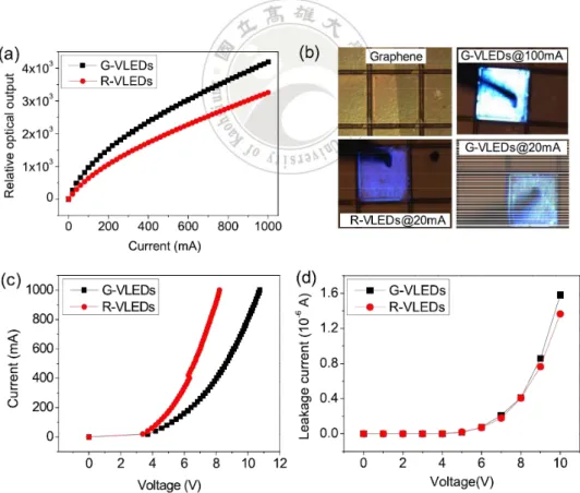
In Figure 1.4a, a stronger light output of graphene VLEDs (G-VLEDs) compared with ITO TCL (R-VLEDs) is observed [6]. In Figure 1.4b, the light output enhancement of G-VLEDs can be attributed to the higher conductivity of graphene than that of u-GaN. Due to the injection current spreading characteristics of graphene, G-VLEDs have uniform current distribution. Under higher injection level, the current crowding effect becomes more prominent in LEDs. Incorporating graphene into VLED effectively elevates the current crowding effect and thus improve the overall performance of VLED. As shown in Figure 1.4c, the higher operating voltage of G-VLEDs is due to the large contact resistance and the work function difference between graphene and u-GaN. As shown in Figure 1.4d, G-VLEDs show good reverse characteristics before and after annealing [6].
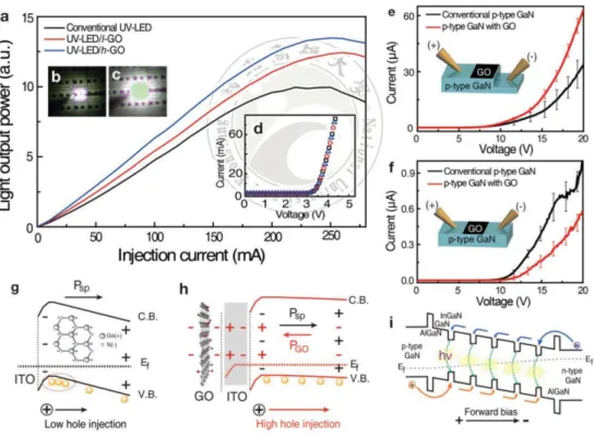
Spontaneous polarization of p-GaN can be suppressed by graphene oxide (GO) passivation in GaN UV LED [9]. The UV-LED including the GO nanosheets is shown in Figure 1.5a [10]. A LED chip with GO/ITO as a TCL and Cr/Au as a p-n electrode is shown in Figure 1.5b [10].
As shown in Figure 1.6a, the light output power of UV-LED/l-GO was enhanced. This was more significant for UV-LED/h-GO [10]. The vertical source-drain hole current was enhanced with GO passivation (Figure 1.6e). This is a direct evidence of the reduced spontaneous polarization. The negative charges at the surface of p-GaN are compensated by the induced positive charges (Figures 1.6g and 1.6h). The effect of charge compensation was
3
also visible in the in-plane source-drain current (Figure 1.6f). In this case, due to the gating effect of the reduced negative charges at the p-GaN surface, the in-plane hole current was reduced. Therefore, more hole carriers are injected to the active region.
Local charge distributions near p-GaN are depicted in Figure 1.6g [10]. Holes in the valence band of p-GaN are bound at the ITO/p-GaN interface, suppressing hole injection into the active layer. GO passivation creates dipole field outside ITO/p-GaN layer and induces positive charges at the surface of p-GaN. This dipole field is opposite of the spontaneous electric polarization (Figure. 1.6h), suppressing internal polarization field in p-GaN. Hole carriers are injected efficiently into active layer to enhance light output power [10, 11]. This concept is shown in Figure 1.6i.
Figure 1.7 (a) shows ultra-violet photoemission spectra (UPS) of as-grown and doped graphene films around the secondary-electron cutoff region and the Fermi level position [12]. Fig. 7(b) reveals the modification of energy band diagram at graphene/p-GaN interface. The reduced difference in the value of ф is estimated from the secondary electron cutoff using the relation ф= Hv- (Ef-Ecutoff) after doping lowers the barrier height at the interface, which improves hole injection into p-GaN [13, 14].
1.2 Motivation
The use of multiple layer graphene as a TCL has limitations for current injection due to the difference of work function between multilayer graphene and p-GaN layer and high sheet resistance. Also, the carrier transport and carrier dynamics behaviors of InGaN/GaN LEDs with multilayer graphene as transparent and current spreading electrodes are not clear. To increase the current injection to GaN-based LEDs, the device characteristics and carrier transport properties of InGaN/GaN LEDs with multilayer graphene as transparent and current spreading electrodes should be investigated.
4
1.3 Device characteristics and carrier transport properties of InGaN/GaN MQW LEDs without and with multilayer graphene transparent electrodes on the p-layer
1.3.1 Investigation procedures and sample preparation
Figure 1.8 shows the experimental procedures. First, before the transformation of graphene onto the p-GaN layer of the InGaN/GaN MQW LEDs, three conventional InGaN/GaN LEDs (namely LED1, LED2, and LED3) were prepared for the measurements of device characteristics. Second, optical microscope images, EL images, electroluminescence (EL), current-voltage (I-V Curve), external quantum efficiency (EQE), and time-resolved electroluminescence (TREL) measurements were conducted on three conventional InGaN/GaN LEDs. Third, graphene was transferred onto the p-GaN layer of the three InGaN/GaN LEDs (corresponding to LED1Gp, LED2Gp, and LED3Gp, respectively). Optical microscope images, EL images, electroluminescence (EL), current-voltage (I-V Curve), external quantum efficiency (EQE), and time-resolved electroluminescence (TREL) measurements were conducted on the three InGaN/GaN LEDs with the graphene transparent conductive electrodes [15, 16]. Forth, device characteristics and carrier transport properties of InGaN/GaN MQWs LEDs without and with multilayer graphene transparent electrodes onto the p-GaN layer were compared.
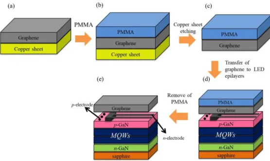
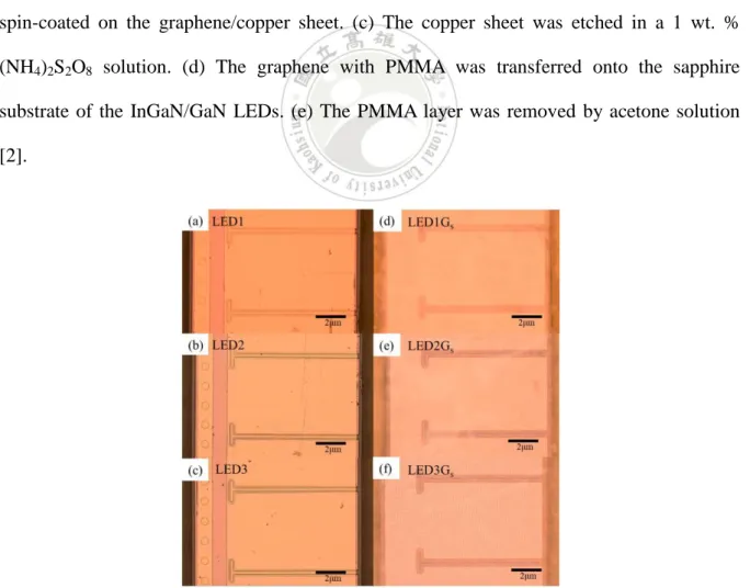
Figure 1.9 shows the fabrication processes of the InGaN/GaN LEDs with the graphene transparent conductive electrodes to the p-GaN layer: (a) Graphene was grown on a copper sheet by a chemical vapor deposition (CVD). (b) Poly (methyl methacrylate) (PMMA) was spin-coated on the graphene/copper sheet. (c) The copper sheet was etched in a 1 wt. % (NH4)2S2O8 solution [2]. (d) The graphene with PMMA was transferred onto the p-GaN layer of the InGaN/GaN LEDs. (e) The PMMA layer was removed by acetone solution.
1.3.2 Optical microscope images study
5
samples LED1, LED2, LED3, LED1Gp, LED2Gp, and LED3Gp, respectively. The positive (p) and negative (n) electrodes can be clearly seen. Graphene can be identified from optical microscope images of the samples LED1Gp, LED2Gp, and LED3Gp, as shown in Figure 1.10 (d), (e) and (f), respectively.
1.3.3 EL images and EL spectra studies
A source meter (Keithley 2614B) was used to apply voltages to the LEDs. The EL images were acquired with CCD (moticam 2000) at room temperature.
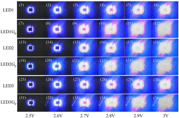
The EL images are shown in Figures 1.11(1)-(6), (7)-(12), (13)-(18), (19)-(24), (25)-(30), and (31)-(36) with applied voltage 2.5, 2.6, 2.7, 2.8, 2.9, and 3.0 Volt at room temperature for the samples LED1, LED1Gp, LED2, LED2Gp, LED3, and LED3Gp, respectively. Several phenomena are observed in the Figure 1.11. First, the LED1Gp, LED2Gp, and LED3Gp are brighter than LED1, LED2, and LED3. The light emitting area of LED1Gp, LED2Gp, and LED3Gp are larger than LED1, LED2, and LED3.
Figure 1.12 shows the experimental setup and schematic diagram of the EL measurement. A source meter (Keithley 2614B) is used to apply voltage to the LED devices. The luminescence from each LED sample is collected by the integrating sphere and focused into a spectrometer with a USB interface (Ocean Optics USB 2000+, resolution 0.3 nm). The EL spectra is subsequently analyzed by a computer.
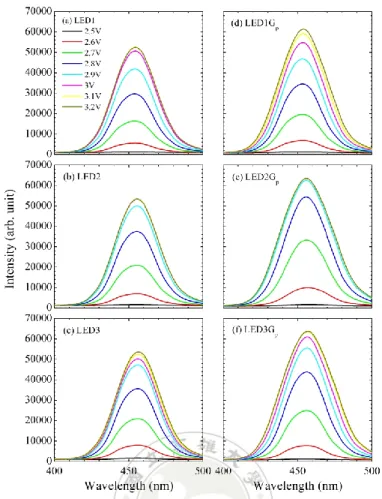
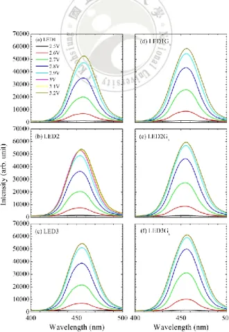
Figures 1.13 (a), (b), (c), (d), (e) and (f) show the EL spectra of the samples LED1, LED2, LED3, LED1Gp, LED2Gp, and LED3Gp at room temperature with 2.5-3.2 V applied voltages, respectively. With higher applied voltages, the all LEDs show stronger EL intensities. Each EL spectrum of the samples LED1, LED2, LED3, LED1Gp, LED2Gp, and LED3Gp only have one peak. Because the FWHM can be defined as the quality of the LED, the quality of the samples LED1Gp, LED2Gp, and LED3Gp are better than that of the LED1, LED2, and LED3.
6
Figure 1.14 shows the peak position of EL spectra as a function of applied voltage for the six LEDs. With high applied voltages, the EL peak positions of the samples LED1Gp, LED2Gp, and LED3Gp, LED1, LED2, and LED3 are slightly blue-shifted.
1.3.4 Current density, output power, and EQE studies
Figure 1.15 (a), (b), (c) show current density (I) as functions of applied voltage (V) for the samples LED1 and LED1Gp, LED2 and LED2Gp, and LED3 and LED3Gp, respectively. With graphene transparent electrodes, the current densities of the LED1Gp, LED2Gp, and LED3Gp are all larger than that of the LED1, LED2, and LED3.
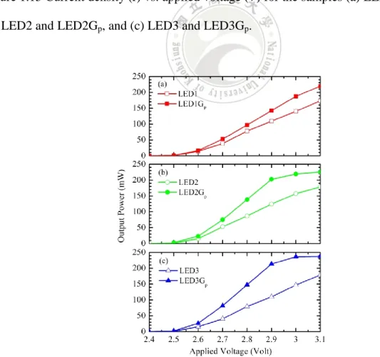
Figure 1.16 (a), (b), (c) show the output power as functions of applied voltage (V) for the samples LED1 and LED1Gp, LED2 and LED2Gp, and LED3 and LED3Gp, respectively. The output power of the LEDs can be measured by a power meter (Newport Model 835).The output powers of the samples LED1Gp, LED2Gp, and LED3Gp are much higher than those of the samples LED1, LED2, and LED3.
Figure 1.17 (a), (b), (c) show the output power as functions of applied current (I) for the samples LED1 and LED1Gp, LED2 and LED2Gp, and LED3 and LED3Gp, respectively. The output powers of the samples LED1Gp, LED2Gp, and LED3Gp are much higher than those of the LED1, LED2, and LED3. This advantage shows great potentials of graphene transparent conductive electrodes in InGaN/GaN MQW LEDs.
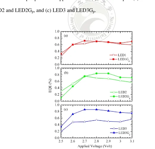
Figure 1.18 (a), (b), (c) show external quantum efficiency (EQE) as functions of applied voltage (V) for the samples LED1 and LED1Gp, LED2 and LED2Gp, and LED3 and LED3Gp, respectively. The external quantum efficiency (EQE) is defined by output power divided by the product of I*V. The EQEs of the samples LED1Gp, LED2Gp, and LED3Gp are higher than those of the LED1, LED2, and LED3. This characteristic shows that graphene acting as transparent conductive electrodes in InGaN/GaN MQW LEDs can improve device performance.
7
1.3.5 Time-resolved Electroluminescence (TREL) Study
In order to understand the carrier transport and recombination dynamics of the InGaN/GaN MQW LEDs without and with graphene transparent electrodes, TREL measurement was conducted.
Figure 1.19 shows experimental setup and schematic diagram of TREL. The probe station can touch the electrodes by the probe. A pulse generator (Tektronix, AFC3011C) is used to apply 3.0-4.2V, 500ns pulse width, and 1kHz repetition rate applied pulse voltages to the devices. The emitting light of LEDs is focused by lens into the detector. Time-dependent EL signals are detected by the 50 Ω input resistance of a digital oscilloscope (Agilent, model DSO 6052A, 500 MHz/4Gs/s) together with a photomultiplier (Photo sensor Modules H10721 Series) located on top of the emitting areas.
Figure 1.20 (a), (b), (c), (d), (e) and (f) show the TREL transit profiles of the samples LED1, LED2, LED3, LED1Gp, LED2Gp, and LED3Gp, respectively. With a larger applied pulse voltage, the rise profile exhibits a stronger intensity and the response time is shorter. The intensities of the samples LED1Gp, LED2Gp, and LED3Gp are stronger than those of the LED1, LED2, and LED3. The samples LED1Gp, LED2Gp, and LED3Gp rises more steeply than the samples LED1, LED2, and LED3.
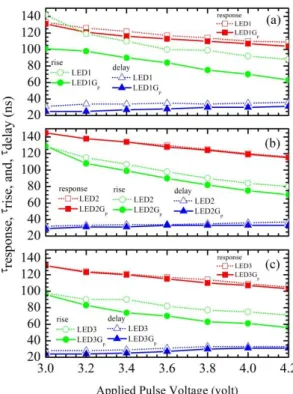
Figure 1.21 (a), (b) and (c) show the response, rise, and delay times as a function of applied pulse voltage for the samples LED1 and LED1Gp, LED2 and LED2Gp, and LED3 and LED3Gp, respectively. The response time (response) can be determined by the time delay between addressing the device with a short voltage pulse and the first appearance of EL. Because a larger forward bias enhances the ability of the hole and electron leading fronts to meet faster more easily, a shorter response time is observed. The shorter response times of the samples LED1Gp, LED2Gp, and LED3Gp imply a better carrier injection efficiency.
8
The rising time (
rise) is defined by intercept of the tangents. The
rise of the samples LED1Gp, LED2Gp, and LED3Gp are shorter than those of the LED1, LED2, and LED3 for each applied voltage. This could also be determined by carrier localization, the strength of QCSE, and the height of potential barrier.The delay time (delay) when the voltage pulse is switched off, TREL transit profiles of the InGaN/GaN MQW LED1, LED2, and LED3 show longer delay time (delay) in reaching both the intensity of transit EL and the subsequent recombination. Due to the combined effects of the weaker carrier localization, stronger QCSE, and the potential barrier, the poorer relaxation efficiency of the samples LED1, LED2, and LED3 needs more time to reach the intensity of transit EL.
Figure 1.22 (a), (b) and (c) show the recombination time as a function of applied pulse voltage for the samples LED1 and LED1Gp, LED2 and LED2Gp, and LED3 and LED3Gp, respectively. The recombination time can be determined by fitting the TREL decay profile with a single exponential. The recombination of the samples LED1Gp, LED2Gp, and LED3Gp are longer than those of the samples LED1, LED2, and LED3 for each applied pulse voltage. The longer recombination of the samples LED1Gp, LED2Gp, and LED3Gp implies a slower carrier recombination. The samples LED1Gp, LED2Gp, and LED3Gp have more carrier injection than the samples LED1, LED2, and LED3, so the samples LED1Gp, LED2Gp, and LED3Gp need more time for carrier recombination.
1.4 Device characteristics and carrier transport properties of InGaN/GaN MQW LEDs without and with multilayer graphene transparent electrodes on the sapphire substrate 1.4.1 Investigation procedures and sample preparation
For comparisons, graphene was also transferred onto the sapphire substrate of the InGaN/GaN LEDs. Figure 1.23 shows the experimental procedures. First, before the
9
transformation of graphene onto the sapphire substrate of the InGaN/GaN LEDs, three conventional InGaN/GaN LEDs (namely LED1, LED2, and LED3) were prepared for the measurements of device characteristics. Second, optical microscope images, EL images, electroluminescence (EL), current-voltage (I-V Curve), external quantum efficiency (EQE), and time-resolved electroluminescence (TREL) measurements were conducted on three conventional InGaN/GaN LEDs. Third, graphene was transferred onto the sapphire substrate of the three InGaN/GaN LEDs (corresponding to LED1Gs, LED2Gs, and LED3Gs, respectively). Optical microscope images, EL images, electroluminescence (EL), current-voltage (I-V Curve), external quantum efficiency (EQE), and time-resolved electroluminescence (TREL) measurements were conducted on the three InGaN/GaN LEDs with the graphene transparent conductive electrodes. Forth, device characteristics and carrier transport properties of InGaN/GaN MQWs LEDs without and with multilayer graphene transparent electrodes onto the p-layer were compared.
Figure 1.24 shows sample structures fabrication processes of the InGaN/GaN LEDs with the graphene transparent conductive electrodes onto the sapphire substrate:(a) Graphene was grown on a copper sheet by a chemical vapor deposition (CVD). (b) Poly (methyl methacrylate) (PMMA) was spin-coated on the graphene/copper sheet. (c) The copper sheet was etched in a 1 wt. % (NH4)2S2O8 solution. (d) The graphene with PMMA was transferred onto the sapphire substrate of the InGaN/GaN LEDs. (e) The PMMA layer was removed by acetone solution.
1.4.2 Optical microscope images study
Figure 1.25 (a), (b), (c), (d), (e) and (f) show the optical microscope images for the samples LED1, LED2, LED3, LED1Gs, LED2Gs, and LED3Gs, respectively. In Figs. (a)-(c), the positive and negative electrodes are shown. Graphene can be identified from optical microscope images of the samples LED1Gs, LED2Gs, and LED3Gs, as shown in Figure 1.25
10
(d), (e) and (f), respectively.
1.4.3 EL images and EL spectra studies
The EL images are shown in Figures 1.26(1)-(6), (7)-(12), (13)-(18), (19)-(24), (25)-(30), and (31)-(36) with applied voltages 2.5, 2.6, 2.7, 2.8, 2.9, and 3.0 Volt at room temperature for the samples LED1, LED1Gs, LED2, LED2Gs, LED3, and LED3Gs, respectively. First, the samples LED1Gs, LED2Gs, and LED3Gs are brighter than the samples LED1, LED2, and LED3. The light emitting area of the samples LED1Gs, LED2Gs, and LED3Gs are larger than the samples LED1, LED2, and LED3.
Figures 1.27 (a), (b), (c), (d), (e) and (f) show the EL spectra of the samples LED1, LED2, LED3, LED1Gs, LED2Gs, and LED3Gs at room temperature with 2.5-3.2 V applied voltages, respectively. With higher applied voltages, the all LEDs show stronger EL intensities. Each EL spectrum of the samples LED1, LED2, LED3, LED1Gs, LED2Gs, and LED3Gs only have one peak. Because the FWHM can be defined as the quality of the LED, the quality of the samples LED1Gs, LED2Gs, and LED3Gs are better than that of the LED1, LED2, and LED3.
Figure 1.28 shows the peak position of EL spectra as a function of applied voltage for the six LEDs. With high applied voltages, the EL peak positions of the samples LED1, LED2, LED3, LED1Gs, LED2Gs, and LED3Gs are slightly shifted.
1.4.4 Current density, output power, and EQE studies
Figure 1.29 (a), (b), (c) show current density (I) as functions of applied voltage (V) for the samples LED1 and LED1Gs, LED2 and LED2Gs, and LED3 and LED3Gs, respectively. With graphene transparent electrodes, the current densities of the LED1Gs, LED2Gs, and LED3Gs are all larger than those of the LED1, LED2, and LED3.
11
the samples LED1 and LED1Gs, LED2 and LED2Gs, and LED3 and LED3Gs, respectively. The output powers of the samples LED1Gs, LED2Gs, and LED3Gs are much higher than those of the samples LED1, LED2, and LED3.
Figure 1.31 (a), (b), (c) show the output power as functions of applied current (I) for the samples LED1 and LED1Gs, LED2 and LED2Gs, and LED3 and LED3Gs, respectively. The output powers of the samples LED1Gs, LED2Gs, and LED3Gs are much higher than those of the LED1, LED2, and LED3.
Figure 1.32 (a), (b), (c) show external quantum efficiency (EQE) as functions of applied voltage (V) for the samples LED1 and LED1Gs, LED2 and LED2Gs, and LED3 and LED3Gs, respectively. The external quantum efficiency (EQE) is defined by output power divided by the product of I*V. The EQEs of the samples LED1Gs, LED2Gs, and LED3Gs are higher than those of the LED1, LED2, and LED3.
1.4.5 Time-resolved Electroluminescence (TREL) Study
Figure 1.33 (a), (b), (c), (d), (e) and (f) show the TREL transit profiles of the samples LED1, LED2, LED3, LED1Gs, LED2Gs, and LED3Gs, respectively. With a larger applied pulse voltage, the rise profile exhibits a stronger intensity and the response time is shorter. The intensities of the samples LED1Gs, LED2Gs, and LED3Gs are stronger than those of the LED1, LED2, and LED3. The samples LED1Gs, LED2Gs, and LED3Gs rises more steeply than the samples LED1, LED2, and LED3.
Figure 1.34 (a), (b) and (c) show the response, rise, and delay times as a function of applied pulse voltage for the samples LED1 and LED1Gs, LED2 and LED2Gs, and LED3 and LED3Gs, respectively. The response time (response) can be determined by the time delay between addressing the device with a short voltage pulse and the first appearance of EL. Because a larger forward bias enhances the ability of the hole and electron leading fronts to
12
meet faster more easily, a shorter response time is observed. The shorter response times of the samples LED1Gs, LED2Gs, and LED3Gs imply a better carrier injection efficiency.
The rising time (
rise) is defined by intercept of the tangents. The
rise of the samples LED1Gs, LED2Gs, and LED3Gs are shorter than those of the LED1, LED2, and LED3 for each applied voltage. This could also be determined by carrier localization, the strength of QCSE, and the height of potential barrier.The delay time (delay) can be determined, when the voltage pulse is switched off. TREL transit profiles of the samples LED1, LED2, and LED3 show longer delay time
)
(delay in reaching both the intensity of transit EL and the subsequent recombination. Due to the combined effects of the weaker carrier localization, stronger QCSE, and the potential barrier, the poorer relaxation efficiency of the samples LED1, LED2, and LED3 needs more time to reach the intensity of transit EL.
Figure 1.35 (a), (b) and (c) show the recombination time as a function of applied pulse voltage for the samples LED1 and LED1Gs, LED2 and LED2Gs, and LED3 and LED3Gs, respectively. The recombination time can be determined by fitting the TREL decay profile with a single exponential. The recombination of the samples LED1Gs, LED2Gs, and LED3Gs are longer than those of the samples LED1, LED2, and LED3 for each applied pulse voltage. The longer recombination of the samples LED1Gs, LED2Gs, and LED3Gs implies a slower carrier recombination. With a larger applied pulse voltage, the samples LED1Gs, LED2Gs, and LED3Gs has more carrier injection than the samples LED1, LED2, and LED3, so the samples LED1Gs, LED2Gs, and LED3Gs need more time for carrier recombination.
1.5 Discussion and summary
In summary, we have demonstrated experimental results of optical microscopy images, EL images, EL spectrum, current density, output power, EQE, and TREL measurements of
13
InGaN/GaN MQW LEDs with multilayer graphene transparent electrodes on the p-layer and on the sapphire substrate. Optical and electrical performances were found to be greatly enhanced by employing graphene as transparent conductive electrodes on the p-layer and on the sapphire substrate in LEDs.
In the first part, optical and electrical performances were greatly enhanced by employing graphene as transparent conductive electrodes on the p-layer of GaN-based LEDs. The EL intensity, current density, output power, and EQE of the GaN-based LEDs with a graphene transparent conductive electrode on the p-layer can be enhanced as high as 18, 10, 26, and 15 %, respectively. In TREL measurement, the shorter response, rise, and delay times of the GaN-based LEDs with a graphene transparent conductive electrode provide more efficient carrier injection, transport, and relaxation. The LEDs with multilayer graphene transparent electrodes on the p-layer have more carrier injection than those without multilayer graphene transparent electrodes on the p-layer, so the LEDs need more time for carrier recombination and show a longer recombination time.
In the second part, optical and electrical performances were also enhanced by employing graphene as transparent conductive electrodes on the sapphire substrate in GaN-based LEDs. The EL intensity, current density, output power, and EQE of the GaN-based LEDs with a graphene transparent conductive electrode on the sapphire substrate can be enhanced as high as 12, 10, 12, and 12 %, respectively. The shorter response, rise, and delay times of the GaN-based LEDs with a graphene transparent conductive electrode provide more efficient carrier injection, transport, and relaxation. The GaN-based LEDs with multilayer graphene transparent electrodes on the sapphire substrate have more carrier injection than those without multilayer graphene transparent electrodes on the sapphire substrate, so the GaN-based LEDs need more time for carrier recombination and show a longer recombination time.
14
sapphire substrate of InGaN/GaN MQW LEDs can effectively enhance device performance, carrier transport, and luminous efficiency. These advantages show great potentials of graphene transparent conductive electrodes in InGaN/GaN MQW LEDs.
15
References
1. A. K. Geim, and K. S. Novoselov, Nat. Mater. 6, 183-191 (2007).
2. B. J. Kim, G. Yang, M. J. Park, J. S. Kwak, K. H. Baik, D. Kim, and J. Kim, Appl. Phys. Lett. 102, 161902 (2013).
3. X. Li, L. Tao, Z. Chen, H. Fang, X. Li, X. Wang, J. B. Xu, and H. Zhu, Appl. Phys. Rev. 4, 021306 (2017).
4. K. S. Novoselov, A. K. Geim, S. V. Morozov, D. Jiang, Y. Zhang, S. V. Dubonos, I. V. Grigorieva, and A. A. Firsov, Science 306, 666-669 (2004).
5. K. S. Novoselov, V. I. Fal′ko, L. Colombo, P. R. Gellert, M. G. Schwab, and K. Kim, Nature 490, 192-200 (2012).
6. L. Wang, Y. Zhang, X. Li, Z. Liu, E. Guo, X. Yi, J. Wang, H. Zhu, and G. Wang, Appl. Phys. Lett. 101, 061102 (2012).
7. K. Xu, C. Xu, Y. Xie, J. Deng, Y. Zhu, W. Guo, M. Mao, M. Xun, M. Chen, L. Zheng, and J. Sun, Appl. Phys. Lett. 103, 222105 (2013).
8. K. Xu, C. Xu, J. Deng, Y. X. Zhu, W. L. Guo, M. M. Mao, L. Zheng, and J. Sun, Appl. Phys. Lett. 102, 162102 (2013).
9. W. S. Hummers, and R. E. Offeman, J. Am. Chem. Soc. 80, 1339 (1958).
10. H. Jeong, S. Y. Jeong, D. J. Park, H. J. Jeong, J. T. Han, H. J. Jeong, S. Yang, H. Y. Kim, K. J. Baeg, S. J. Park, Y. H. Ahn, E. K. Suh, G. W. Lee, Y. H. Lee, and M. S. Jeong, Sci. Rep. 5, 7778 (2015).
11. S. Jung, K. R. Song, S. N. Lee, and H. Kim, Adv. Mater. 25, 4470-4476 (2013).
12. H. J. Shin, W. M. Choi, D. Choi, G. H. Han, S. M. Yoon, H. K. Park, S. W. Kim, Y. W. Jin, S. Y. Lee, J. M. Kim, J. Y. Choi, and Y. H. Lee, J. Am. Chem. Soc. 132, 15603 (2010).
13. D. Ziegler, P. Gava, J. Guttinger, F. Molitor, L. Wirtz, M. Lazzeri, A. M. Saitta, A. Stemmer, F. Mauri, and C. Stampfer, Phys. Rev. B 83, 235434 (2011).
16
14. S. Chandramohan, J. H. Kang, Y. S. Katharria, N. Han, Y S. Beak, K. B. Ko, J. B. Park, H. K. Kim, E. K. Suh, and C. H. Hong, Appl. Phys. Lett. 100, 023502 (2012).
15. S. W. Feng, P. H. Liao, B. Leung, J. Han, F. W. Yang, and H. C. Wang, J. Appl.Phys. 118, 043104, (2015).
17
Figure 1.1 The applications of graphene [1-4]
; Figure 1.2 The quality and production cost of various kinds of graphene [5].
18
Figure 1.3 Schematic diagram of the G-VLED fabrication process [6].
Figure 1.4 (a) Light output vs. current for G-VLEDs and R-VLEDs. (b) EL image of G-VLEDs. (c) Current-voltage characteristics of G-VLEDs and R-VLEDs before annealing; (d) Leakage current of G-VLEDs and R-VLEDs before annealing [6].
19
Figure 1.5 (a) GaN-based UV-LED structures, and (b) fabricated device covered with GO nanosheets [10].
Figure 1.6 (a) Light output power vs. current of conventional, l-GO-passivated, and h-GO-passivated UV-LEDs. (d)I-V cures of p-GaN with and without GO nanosheets measured by (e)vertical and (f)in-plane configuration. Higher (lower) current in vertical (in-plane) configuration was observed from p-GaN with GO compared to that without GO. Energy band diagram of p-GaN (g)without and (h)with h-GO. (i) Schematic energy band diagram of active region in UV-LED with applied forward bias [10].
20
Figure 1.7 (a) UPS spectra of as-grown and doped graphene films around the secondary-electron cutoff region and the Fermi level position. (b)Energy band diagram at the graphene/p-GaN interface [12-14].
21
Figure 1.8 Experimental flow chart of this chapter [15, 16]. Three conventional InGaN/GaN LEDs
(namely LED1, LED2, and LED3) were prepared.
Sample preparation LEDs (namely LED1, LED2, and LED3)
Optical microscope images, EL images, electroluminescence (EL), current-voltage
(I-V Curve), external quantum efficiency (EQE), and time-resolved
electroluminescence (TREL) measurements were conducted on three
conventional InGaN/GaN LEDs.
The graphene was transferred onto the
p-GaN layer of the three InGaN/GaN
LEDs (corresponding to LED1Gp, LED2Gp, and LED3Gp, respectively).
Optical microscope images, EL images, EL, I-V, EQE, and TREL measurements were conducted on the three InGaN/GaN
LEDs with the graphene transparent conductive electrodes
Device characteristics and carrier transport properties of InGaN/GaN
MQWs LEDs without and with multilayer graphene transparent electrodes on the p-layer were compared.
Device characteristics and carrier transport properties of InGaN/GaN
MQWs LEDs without multilayer graphene transparent electrodes
Sample preparation of InGaN/GaN MQWs LEDs with multilayer graphene transparent electrodes on the p-GaN layer (corresponding to LED1Gp, LED2Gp, and LED3Gp,
respectively)
Comparisons of device characteristics and carrier transport
properties of InGaN/GaN MQWs LEDs without and with multilayer graphene transparent electrodes on
the p-layer
Device characteristics and carrier transport properties of InGaN/GaN
MQWs LEDs with multilayer graphene transparent electrodes.
22
Figure 1.9 Fabrication processes of the InGaN/GaN LEDs with the graphene transparent conductive electrodes on the p-GaN layer:(a) Graphene was grown on a copper sheet by a chemical vapor deposition (CVD). (b) Poly(methyl methacrylate) (PMMA) was spin-coated on the graphene/copper sheet. (c) The copper sheet was etched in a 1 wt. % (NH4)2S2O8 solution [2]. (d) The graphene with PMMA was transferred onto the p-GaN layer of the InGaN/GaN LEDs. (e) The PMMA layer was removed by acetone solution.
Figure 1.10 Optical microscope images of the samples (a) LED1, (b) LED2, (c) LED3, (d) LED1Gp, (e) LED2Gp, and (f) LED3Gp.
23
Figure 1.11 EL images for the samples (1)~(6) LED1, (7)~(12) LED1Gp, (13)~(18) LED2, (19)~(24) LED2Gp, (25)~(30) LED3, and (31)~(36) LED3Gp with the excitations of 2.5, 2.6, 2.7, 2.8, 2.9, and 3.0 Volt electron voltages under room temperature, respectively.
24
Figure 1.13 EL spectra as a function of applied voltages for the samples (a) LED1, (b) LED2, (c) LED3, (d) LED1Gp, (e) LED2Gp, and (f) LED3Gp at room temperature.
Figure 1.14 EL peak position as a function of applied voltages for the samples LED1, LED2, LED3, LED1Gp, LED2Gp, and LED3Gp at room temperature.
25
Figure 1.15 Current density (I) vs. applied voltage (V) for the samples (a) LED1 and LED1Gp, (b) LED2 and LED2Gp, and (c) LED3 and LED3Gp.
Figure 1.16 Output power vs. applied voltage (V) for the samples (a) LED1 and LED1Gp, (b) LED2 and LED2Gp, and (c) LED3 and LED3Gp.
26
Figure 1.17 Output power vs. applied current (I) for the samples (a) LED1 and LED1Gp, (b) LED2 and LED2Gp, and (c) LED3 and LED3Gp.
Figure 1.18 External quantum efficiency (EQE) as functions of applied voltage (V) for the samples (a) LED1 and LED1Gp, (b) LED2 and LED2Gp, and (c) LED3 and LED3Gp.
27
Figure 1.19 Experimental setup of TREL measurement.
Figure 1.20 TREL profiles of the samples (a) LED1, (b) LED2, (c) LED3, (d) LED1Gp, (e) LED2Gp, and (f) LED3Gp at room temperature.
28
Figure 1.21 Response, rise, and delay times as a function of applied pulse voltage for the samples (a) LED1 and LED1Gp, (b) LED2 and LED2Gp, and (c) LED3 and LED3Gp.
Figure 1.22 Recombination time as a function of applied pulse voltage for the samples (a) LED1 and LED1Gp, (b) LED2 and LED2Gp, and (c) LED3 and LED3Gp.
29
Figure 1.23 Experimental flow chart of this chapter. Three conventional InGaN/GaN LEDs
(namely LED1, LED2, and LED3) were prepared.
Sample preparation
Optical microscope images, EL images, EL, I-V, EQE, and TREL measurements were conducted on three conventional
InGaN/GaN LEDs.
The graphene was transferred onto the sapphire substrate of the three InGaN/GaN
LEDs (corresponding to LED1Gs, LED2Gs, and LED3Gs, respectively).
Optical microscope images, EL images, EL, I-V, EQE, and TREL measurements were conducted on the three InGaN/GaN
LEDs with the graphene transparent conductive electrodes
Device characteristics and carrier transport properties of InGaN/GaN MQWs LEDs
without and with multilayer graphene transparent electrodes onto the sapphire
substrate were compared.
Device characteristics and carrier transport properties of InGaN/GaN
MQWs LEDs without multilayer graphene transparent electrodes
Sample preparation of InGaN/GaN MQWs LEDs with multilayer graphene transparent electrodes on
the sapphire substrate (corresponding to LED1Gs,
LED2Gs, and LED3Gs, respectively)
Comparisons of device characteristics and carrier transport
properties of InGaN/GaN MQWs LEDs without and with multilayer graphene transparent electrodes on
the sapphire substrate Device characteristics and carrier transport properties of InGaN/GaN
MQWs LEDs with multilayer graphene transparent electrodes
30
Figure 1.24 Fabrication processes of the InGaN/GaN LEDs with the graphene transparent conductive electrodes on the sapphire substrate:(a) Graphene was grown on a copper sheet by a chemical vapor deposition (CVD). (b) Poly(methyl methacrylate) (PMMA) was spin-coated on the graphene/copper sheet. (c) The copper sheet was etched in a 1 wt. % (NH4)2S2O8 solution. (d) The graphene with PMMA was transferred onto the sapphire substrate of the InGaN/GaN LEDs. (e) The PMMA layer was removed by acetone solution [2].
Figure 1.25 Optical microscope images of the samples (a) LED1, (b) LED2, (c) LED3, (d) LED1Gs, (e) LED2Gs, and (f) LED3Gs.
31
Figure 1.26 EL images for the samples (1)~(6) LED1, (7)~(12) LED1Gs, (13)~(18) LED2, (19)~(24) LED2Gs, (25)~(30) LED3, and (31)~(36) LED3Gs with the excitations of 2.5, 2.6, 2.7, 2.8, 2.9, and 3.0 Volt electron voltages under room temperature, respectively.
Figure 1.27 EL spectra as a function of applied voltages for the samples (a) LED1, (b) LED2, (c) LED3, (d) LED1Gs, (e) LED2Gs, and (f) LED3Gs at room temperature.
32
Figure 1.28 EL peak position as a function of applied voltages for the samples LED1, LED2, LED3, LED1Gs, LED2Gs, and LED3s at room temperature.
Figure 1.29 Current density (I) vs. applied voltage (V) for the samples (a) LED1 and LED1Gs, (b) LED2 and LED2Gs, and (c) LED3 and LED3Gs.
33
Figure 1.30 Output power vs. applied voltage (V) for the samples (a) LED1 and LED1Gs, (b) LED2 and LED2Gs, and (c) LED3 and LED3Gs.
Figure 1.31 Output power vs. applied current (I) for the samples (a) LED1 and LED1Gs, (b) LED2 and LED2Gs, and (c) LED3 and LED3Gs.
34
Figure 1.32 External quantum efficiency (EQE) as functions of applied voltage (V) for the samples (a) LED1 and LED1Gs, (b) LED2 and LED2Gs, and (c) LED3 and LED3Gs.
Figure 1.33 TREL profiles of the samples (a) LED1, (b) LED2, (c) LED3, (d) LED1Gs, (e) LED2Gs, and (f) LED3Gs at room temperature.
35
Figure 1.34 Response, rise, and delay times as a function of applied pulse voltage for the samples (a) LED1 and LED1Gs, (b) LED2 and LED2Gs, and (c) LED3 and LED3Gs.
Figure 1.35 Recombination time as a function of applied pulse voltage for the samples (a) LED1 and LED1Gs, (b) LED2 and LED2Gs, and (c) LED3 and LED3Gs.
36
Chapter 2 Efficient recombination dynamics in InGaN/GaN
multiple-quantum-wells and efficient device performance and carrier
transport in InGaN/GaN LEDs by using multilayer graphene
transparent electrodes
2.1 Introduction
Graphene is considered to be an ideal candidate to replace ITO electrodes because of an excellent transparency to visible light (~97% for monolayer graphene) and high electrical conductivity. Graphene have been used in GaN-based LEDs as transparent electrodes [1]. Meanwhile, the large work function mismatch between graphene (~4.8 eV) and p-GaN (~7.5 eV) leads to a high contact barrier that hindered the movement of electrons and increased the operating voltage of LEDs [2]. To decrease contact resistance of graphene/p-GaN, inserting ITO quantum dots and metal sheets between graphene and p-GaN have been developed [2].
Fig. 2.1 shows the fabrication process of InGaN green light-emitting diodes with graphene transparent conductive electrodes [4-5]: (a) the multi-layer graphene (MLG) was transferred onto the p-GaN layer; (b) applying an inductively coupled plasma (ICP) to etch n-GaN layer [2]; (c) the p- and n- electrodes were fabricated on the MLG layer and the n-GaN layer; (d) structure of a MLG-LED [2, 6-7].
Fig. 2.2a shows the EL image of the LED with and without graphene [2, 3]. Due to the injection current spreading characteristics of graphene, the graphene LED have uniform current distribution. As shown in Fig. 2.2b, the higher operating voltage of graphene LED is due to the large contact resistance and the work function difference between graphene and p-GaN. As shown in Fig. 2.2c, a stronger light output of LED with graphene compared with LED without graphene is observed. As shown in Fig. 2.2d, when the injection current increases, the peak wavelength shift of
37
the graphene LED is faster than that of the LED without graphene [2, 8-10].
2.2 Motivation
By SEM and CL measurement, the microstructures and nano-photonics of samples are measured. By XRD measurements, the indium composition of sample and the peak position of graphene are determined. By AFM measurement, the surface morphologies and roughness of samples are observed. By PL and TRPL measurement, the optical properties of samples are investigated. According to the results of the experiments, we will discuss the material and optical characteristics of InGaN/GaN MQW epilayers with and without multilayer graphene. Also, the carrier transport and carrier dynamics behaviors of InGaN/GaN LEDs with multilayer graphene as transparent and current spreading electrodes are not clear. To increase the current injection to GaN-based LEDs, the device characteristics and carrier transport properties of InGaN/GaN LEDs with multilayer graphene as transparent and current spreading electrodes should be investigated.
2.3 Sample preparations and investigation procedures
Fig. 2.3 shows the experimental procedures. First, before the transformation of graphene onto the p-GaN layer of the InGaN/GaN MQW LEDs, three conventional InGaN/GaN LEDs (namely LED1, LED2, and LED3) were prepared for the measurements of optical and material characteristics. Second, scanning electron microscope (SEM), cathodoluminescence (CL), atomic force microscopy (AFM), x-ray diffraction (XRD), temperature-dependent photoluminescence (PL), and time-resolved photoluminescence (TRPL) measurements were conducted on three conventional InGaN/GaN LEDs [12]. Third, EL images, electroluminescence (EL) spectra, current-voltage (I-V Curve), external quantum efficiency (EQE), and
38
time-resolved electroluminescence (TREL) measurements were conducted on three conventional InGaN/GaN LEDs. Forth, graphene was transferred onto the p-GaN layer of the three InGaN/GaN LEDs (corresponding to LED1G, LED2G, and LED3G, respectively). Fifth, SEM, CL, AFM, XRD, PL and TRPL measurements were conducted on the three InGaN/GaN epilayers with the graphene transparent conductive electrodes. Optical and material characteristics of InGaN/GaN MQW epilayers without and with multilayer graphene transparent electrodes onto the p-GaN layer were compared. Sixth, EL images, EL spectra, I-V Curve, EQE, and TREL measurements were conducted on the three InGaN/GaN LEDs with the graphene transparent conductive electrodes. Device characteristics and carrier transport properties of InGaN/GaN MQW LEDs without and with multilayer graphene were compared.
Fig. 2.4 shows the fabrication processes of the InGaN/GaN LEDs with the graphene transparent conductive electrodes onto the p-GaN layer: (a) Graphene was grown on a copper sheet by a chemical vapor deposition (CVD). (b) Poly (methyl methacrylate) (PMMA) was spin-coated on the graphene/copper sheet. (c) The copper sheet was etched in a 1 wt. % (NH4)2S2O8 solution [11]. (d) The graphene with PMMA was transferred onto the p-GaN layer of the InGaN/GaN LEDs. (e) The PMMA layer was removed by acetone solution.
2.4 Optical and material characteristics of InGaN/GaN MQW epilayers without and with multilayer graphene transparent electrodes on the p-GaN layer
2.4.1 Scanning electron microscope (SEM) and CL spectra studies
Fig. 2.5 (a), (b), (c), (d), (e) and (f) show the SEM images using the 11kV excitation electron voltage for the LED1, LED2, and LED3 samples, respectively.
39
LED2, and LED3 at room temperature with 5.0, 7.0, and 9.0 kV applied voltages, respectively.
2.4.2 Atomic force microscopy (AFM) and x-ray diffraction (XRD) studies
Fig. 2.7 (a), (b), (c), (d), (e) and (f) show the AFM images for the samples LED1, LED2, LED3, LED1G, LED2G, and LED3G, respectively. The growth direction of graphene affects the surface roughness. The surface roughness in 5 μm × 5 μm area are 0.652nm, 0.975nm, 1.069nm, 3.104nm, 4.897nm, and 6.760nm for the samples LED1, LED2, LED3, LED1G, LED2G, and LED3G, respectively. Graphene can be identified from AFM images of the samples LED1G, LED2G, and LED3G, as shown in Fig. 2.7 (d), (e) and (f), respectively.
Fig. 2.8 (a) and (b) show XRD patterns for the samples LED1, LED2, LED3, LED1G, LED2G, and LED3G at room temperature, respectively. The diffraction peaks corresponding to GaN and InGaN can be identified [12]. The GaN diffraction peak is mainly from contact and barrier layers. The side shoulder with a broad distribution below the GaN main peak was attributed to InGaN with various indium contents, sizes, and shapes in the quantum wells. This suggests indium aggregation in the quantum well region. The strongest InGaN diffraction peak of the LED3G among the three samples show the most apparent indium aggregation. LED1G, LED2G, and LED3G show an enhanced indium aggregation.
2.4.3 Temperature-dependent photoluminescence (PL) and time-resolved photoluminescence (TRPL) studies
Fig. 2.9 (a), (b), (c), (d), (e) and (f) show the PL spectra of the samples LED1, LED2, LED3, LED1G, LED2G, and LED3G as a function of temperature, respectively. At low temperatures, all LEDs show stronger PL intensities. The
![HPSH [ 分子間作用力 - 凡得瓦力 ]](data:image/gif;base64,R0lGODlhAQABAIAAAP///wAAACH5BAEAAAAALAAAAAABAAEAAAICRAEAOw==)