行政院國家科學委員會專題研究計畫 成果報告
高輸入動態範圍 CMOS 低電壓電流鏡之設計
研究成果報告(精簡版)
計 畫 類 別 : 個別型 計 畫 編 號 : NSC 97-2221-E-151-047- 執 行 期 間 : 97 年 08 月 01 日至 98 年 09 月 30 日 執 行 單 位 : 國立高雄應用科技大學電子工程系 計 畫 主 持 人 : 王鴻猷 計畫參與人員: 碩士班研究生-兼任助理人員:蔡博仰 碩士班研究生-兼任助理人員:林泱全 報 告 附 件 : 出席國際會議研究心得報告及發表論文 處 理 方 式 : 本計畫涉及專利或其他智慧財產權,2 年後可公開查詢中 華 民 國 99 年 01 月 01 日
行政院國家科學委員會補助專題研究計畫
▓ 成 果 報 告
□期中進度報告
高輸入動態範圍 CMOS 低電壓電流鏡之設計
計畫類別:
▓
個別型計畫 □ 整合型計畫
計畫編號:NSC97-2221-E-151-47
執行期間: 97 年 08 月 01 日至 97 年 09 月 30 日
計畫主持人:王鴻猷
共同主持人:蔣元隆
計畫參與人員:
蔡博仰、林泱全
成果報告類型(依經費核定清單規定繳交):▓精簡報告 □完整報告
本成果報告包括以下應繳交之附件:
▊赴國外出差或研習心得報告一份
□赴大陸地區出差或研習心得報告一份
□出席國際學術會議心得報告及發表之論文各一份
□國際合作研究計畫國外研究報告書一份
處理方式:除產學合作研究計畫、提升產業技術及人才培育研究計畫、列管計畫及
下列情形者外,得立即公開查詢
□涉及專利或其他智慧財產權,□一年▊二年後可公開查詢
執行單位:
國立高雄應用科技大學電子工程系
中 華 民 國
98 年 12 月
21
日
中文摘要:
本計畫主要為高輸入動態範圍低電壓電流鏡之研發,適用於製程技術發展趨勢所需,由於常見的電 流式主動元件,例如可控制電流傳輸器(Controlled Current Conveyor, CCCII), (Four-Terminal Floating Nullor, FTFN)等,其實現均需利用高輸入電流動態範圍低電壓電流鏡,故研發高輸入動態範圍低電壓電 流鏡,將有助於設計高性能電流式主動元件。
關鍵詞:
輸入動態範圍(Input dynamic range)、電流鏡(Current mirror)、CCCII、FTFN。
Abstract:
The main objective of this project is to develop the low voltage current mirrors with larger input dynamic range. It is suitable for the technology development trend. In addition, the popular current-mode active elements, such as Controlled Current Conveyor (CCCII) and Four-Terminal Floating Nullor (FTFN), their realization need the usage of large input current dynamic range low voltage current mirrors. So the research of such current mirror will be helpful for the design of high performance current-mode active elements. Since the CCCII and FTFN are often used for the implementation of the derived circuits that are synthesized with network transformation techniques, the research will conduce the development of analog signal processing circuits. 一、 前言: 傳統上,類比電路均以電壓作為訊號的代表,近年來,電流式類比電路已被接受為電壓式類比電路 以外的另一可考慮的選擇,所謂電流式電路,是指以電流作為信號的代表,以電流信號作為電路的輸出 與輸入變數。電流式電路與電壓式電路的比較上有幾個可能的優異點: (1) 較高的頻寬:雙極性電晶體(BJT)與場效電晶體(FET),都是電流輸出的元件,電流式的訊號處理自 然有較寬頻寬的能力,電晶體構成的電流放大器頻寬幾乎可工作到其單一增益頻寬 fT。 (2) 算術運算上較低的電路複雜度:由於電路的連接對電流而言可以做加減法運算,利用電流鏡(Current Mirror)電路可以很方便的做訊號的放大,相對於電壓式類比電路使用運算放大器來做這些運算而 言,電路複雜度可以降低不少。 (3) 較寬的動態範圍(Dynamic Range):CMOS 積體電路技術的進步使元件尺寸不斷的縮小,電壓源準 位的減小導致電壓式電路動態範圍的縮小,一種克服這問題的方法即將其改變成電流式電路,如此 一來,信號的範圍可不直接受限於電壓準位,而是決定於設計者所選擇的輸入阻抗準位。 (4) 較快的操作速度:在實際電路裡,寄生效應主要是寄生電容所主宰,寄生電容的影響造成電壓無法 快速變動,而電流的變動則不受寄生電容效應的影響。 除了電流式電路受到廣泛的注意外,電流式主動元件亦受到不少的重視,所謂電流式主動元件是指 其輸入與輸出變數包括了電流與電壓變數,這類主動元件包括電流傳輸器(Current Conveyor, CC)、可控 制電流傳輸器(Controlled Current Conveyor, CCCII)、電流回授運算放大器(Current-Feedback Operational Amplifier, CFOA)、運算轉導放大器(Operational transconductance Operational, OTA)、運算浮接放大器 (Operational Floating Amplifier, OFA)等等[2],這類主動元件之所以被使用來設計電路,乃因其輸出輸入 埠具備電流或電壓的變數,可用來設計電流式或電壓式電路,在電路設計時比完全以電壓為變數的主動 元件,例如:運算放大器(Operational Amplifier, Op-Amp),具備更大的設計彈性,因此,很多使用這類 元件的應用電路都被提出 [1-4]。而設計這些主動元件,都需要大動態範圍之電流隨耦器與電壓隨耦器,
因此,本計畫投注於高輸入動態範圍低電壓電流鏡之研發。 二、 研究目的:
現今,由於攜帶式電子產品的需求使得低功率電路設計特別引人注目,降低電源電壓為一直接的方 法去達到低功率消耗,低功率及低電壓CMOS技術廣泛地被應用於類比或混合訊號之IC電路中。電流鏡 (Current Mirror, CM)為無論在類比或混合模式VLSI電路中最常見的基本架構之一,尤其是主動元件像 是運算放大器、電流傳輸器、電流回授放大器…等,電流鏡通常用於產生倍數的輸出以及運作像是主動 負載,它為組成這些元件不可穫缺的部份[5]。 儘管大部份電流鏡電路為理想上有高輸出阻抗及大輸出電壓/電流擺幅 [6-17],在某些應用中,設計 者也感興趣於有大輸入擺幅,例如,CC、CCII、FTFN的X端有線性電流隨耦的特性需要大輸入電流擺 幅進而有大電壓擺幅於實際的應用 [18],本文提出,低功率CMOS疊接電流鏡具有高輸出阻抗及大輸入 輸出訊號擺幅,利用HSPICE模擬驗證提出電路及普遍的低電壓疊接電流鏡 [6, 19],模擬結果證實了我 們理論的推測。 三、 文獻探討: 電流鏡是類比電路之重要功能方塊,相關電流鏡之文獻包括[6-20],大部份電流鏡電路著重於電路 特性具有高輸出阻抗及大輸出電壓/電流擺幅。 四、 研究方法: 由於大輸出電壓擺幅及小輸入電壓的特性與傳統疊接電流鏡比較,低電壓疊接電流鏡[6, 19],如圖 一,值得相當關注在低電壓/低功率電路設計。假設電流鏡M1及M2具有相同的長寬比,也就是AM =W1/L1=W2/L2,當W1, W2, L1及L2分別為電晶體M1及M2通道的長與寬,相同地,疊接電晶體M3及M4假 設有相同的長寬比,AC=W3/L3=W4/L4。基底效應被忽略及假設所有NMOS電晶體有相同的臨界電壓Vth及轉 導參數k。確保M1及M3操作在飽合區,偏壓電壓VB於圖一將 3 ( 1 1) 3 GS GS TN B GS TN V V V V V V (1) 方程式(1)能被用於決定輸入電流範圍 [19]。可表現為 2 2 / 2 ( 2 ) ( 2 ) ( ) 2 2 1 / C M M B tn in M B tn C M A A k k A V V I A V V A A (2) 在圖1中,當Iin增加,VGS3及Vin將增加,因為VB固定,M1汲極端電壓準位減少,因此,M1進入三極區決 定Iin的上限。 位準轉移電流鏡有輸入及輸出的需求之優勢[11, 20]被重繪在圖二,電晶體M5轉移電壓準位於M1的 汲極端。在這電路中輸入順從電壓(Vin1)為一個特徵參數決定輸入電壓擺幅的範圍,偏壓電流(Ibias1)的大
小決定M5操作範圍,輸入電流(Iin1)及外加電壓(VO1)決定M2操作範圍,Ibias1及Iin1決定M1操作範圍。在圖
二中,當Iin1增加,VGS1將增加,由於M5位準轉移的功能,Vin1將增加並且幫助M1操作在飽和區。
提出的電流鏡如圖三,結合低電壓疊接電流鏡與位準轉移電流鏡的技術去達成高輸出阻抗、大輸入 及輸出訊號擺幅。因此,我們命名它為低電壓位準轉移疊接電流鏡,在圖三中,假設鏡射電晶體M1及M2、 疊接電晶體M3及M4有各別地相同長寬比,也就是,W1/L1=W2/L2= AM及 W3/L3=W4/L4= AC為表示在圖一, 基底效應被忽略及假設所有NMOS電晶體有相同的臨界電壓Vtn及Vtp為M5的臨界電壓(長寬比W5/L5=AB), 去開啟電晶體M5及M3,條件必需滿足VSG5>|Vtp| and VGS3>Vtn。因為|Vtp|>Vtn,將困難地去保持這條件VDS3>0 電路有效在於Iin2一廣泛的範圍 [20]。因此,電晶體M5、M3及M1能被操作有很多可能的組合,在研究過各
種狀況,可以發現最適合的工作模式為M5工作在次臨界傳導(sub-threshold)區,當M3及M1工作在次臨界 傳導區為低輸入電流及在飽和區為高輸入電流,考慮M5在次臨界傳導區,VSD5>3VT,M5次臨界汲極電流能 表示為 [20-22] 5 5 2 5 5 exp SG tp bias DO T V V W I I L nV (3)
當VT(室溫電壓可視為26mV)的電壓,,而常數n與IDO5為製程參數。典型的IDO5參數的數值大約為20nA
而n參數大約介於1.2到2.0之間。我們研究出最適合的兩個操作模式如下。 Case1:當輸入電流較小時,M3與M1將會操作在次臨界傳導區。而此電路之電壓來源為 M5之電壓, M1和M3的電壓值幾乎在臨界電壓附近 [20]。我們可以得知 2 5 2 5 2 1 ln in DO B in T SG tn tp bias DO M I I A V nV V V V I I A (4) 2 0Vin Vtn (5) 2 1 3 0Iin min(IDO AM,IDO AC) (6) 在這情況下,電流鏡在M1和M3的次臨界傳導區會產生一極差之頻率響應 [21] 。 Case2:當輸入電壓較大時,M3與M1將會操作在飽和區。我們可以發現到 2 2 2 in in tn M I V V kA (7) 2 1 C tn in tn M A V V V A (8)
在圖3中,因Vin2增加進而Iin2也隨之增加。電晶體M5的電壓將會因M3的電壓改變而改變,因此,此電流
鏡與圖1中之低電壓疊接電流鏡之比較,將可改善輸入電流之上限。輸入電流之上限將可用此方程式表 示 2 2 2 C tn in kA V I (9) Case2的操作模式為我們所提議之低電壓位準轉移疊接電流鏡的最佳模式。因為只有M5操作在次臨界傳 導區而M1-M4被限制操作在飽和區,而此電流鏡與Case1的輸入電流相比擁有較高的頻率響應和較低的 輸入電流。M5在次臨界傳導區並不會影響頻率響應因為M5用來設定dc的操作點。在此之外,在這個操 作模式下,我們所提出之電流鏡之最小的輸出電壓如下: 2,min ( ) 4( ) o DS sat DS sat V V V (10) 此外,輸入之電阻(Rin)與輸出電阻(Rout)可以由下列方程式表示如下 1 1 m Rin g (11) 4 2 4 out m o o R g r r (12)
其 gm1,gm4,ro2 與 ro4 將有其重要性。
因考慮到製程特性|Vtp|>Vtn,在圖3中之Ibias2需要一極小且符合M5再次臨界傳導區和在Case2下之M3之
飽和區。當圖3中之Ibias2太小,使得M3可能操作於工作區,而M1、M2和 M4操作於飽和區。VGS3必須大於VGS4, 已達到M1與M2之鏡像電流。因此,VDS1會小於VDS2。因此,鏡像的電流轉換比的正確性是減少。無論如何, 如果多臨界電壓技術是有用的,可是M1-M4很輕易到操作在飽和區。此外,藉由觀察圖三中電路,我們可 以觀察到互補之版本。而互補的電流鏡具有類似的特性如先前所提到。不論如何,當|Vtp|>Vtn時,可輕 易的實現Case2下的操作模式。 圖2(b)中[11],類似的架構有被提出,並使用位準轉移技術。與圖3中之電流鏡與圖2(b)的[11]比 較。不同的地方由此將被指出。圖3的電路中使用較少的偏壓電流源,是較簡單的架構。圖3中的M5由原 工作在飽和區被改為次臨界傳導區。[7]中的圖2(b)需使用PNP,其互補版本需使用NPN,然而,NPN不方 便於CMOS技術中實現。 模擬結果 驗證提出組態的可能性,低電壓疊接電流鏡 (圖三)及低電壓疊接電流鏡(圖一) 的電路模擬進行基
於TSMC 0.18μm CMOS 技術Level49 MOS model參數,DC供給電壓為 1V。去達成高輸入電流範圍,選
擇VB=0V及Ibias2設定為2.6μA確保M5操作在次臨界傳導區。圖四偏壓電路提供偏壓電流,表一表示電流鏡
及偏壓電路不同電晶體的長寬比。圖五顯示兩種電流鏡之輸入特性曲線。圖六顯示兩種電流鏡之電流轉
換特性曲線,能夠觀察提出之電流鏡有改善輸入動態範圍,以及Iout2與Iin2比值機乎接近於一。圖七及八
分別為提出電流鏡於高及低輸入電流時的輸出特性曲線。對於輸出接地,圖九顯示頻率響應的大小於Iin2 為1mA DC及其值於表二。在實際的應用,輸出將阻抗減少頻寬於電流鏡由於RC效應。 五、 結果與討論: 低電壓位準轉移疊接電流鏡具有大輸出阻抗、大輸出擺幅及增強之輸入動態範圍在本研究被提出, 一個MOS電晶體工作在次臨界傳導區被使用如一位準轉移器,它改善常用低電壓疊接電流鏡輸入擺幅, 其可行性被討論及驗證藉由HSPICE模擬,提出之電路可應用於低功率及低電壓之電路需求。 六、成果自評: 本研究內容與原計畫完全相符,並達成預期目標,研究成果具學術價值,適合在學術期刊發表。 本論文已線上發表於International Journal of Circuit Theory and Applications,資訊如下:
H.Y. Wang, Y.L. Jeang, Y.C. Liu, and Y.W. Huang, “CMOS current mirror with enhanced input dynamic range,” International Journal of Circuit Theory and Applications (2009) Published online in Wiley InterScience. DOI: 10.1002/cta.617(SCI)
參考文獻:
[1] C. TOUMAZOU, F. J. LIDGEY, and D G. HAIGH, , Analogue IC design: the Current-Mode Approach (London: Peter Peregrinus), 1990.
[2] H. SCHMID, “Approximating the universal active element”, IEEE Trans. Circuit and System –II, vol. 47, pp. 1160-1169,2000.
[3] B. NAUTA, Analog CMOS Filters for Very High Frequencies, Kluwer Academic Publishers, 1993. [4] CARLOSENA, and G. S. MOSCHYTZ, “Nullators and norators in voltage to current mode
transformations”, Int. J. Circuit Theory and Applications, vol. 21, pp. 421-424, 1993.
[5] Salem SB, Fakhfakh M, Masmoudi DS, Loulou M, Loumeau P, Masmoudi N. A high performances CMOS CCII and high frequency applications. Analog Integrated Circuits and Signal Processing 2006; 49(1):71–78. 2.
[6] Razavi B. Design of Analog CMOS Integrated Circuit. McGraw-Hill: Boston, 2001.
[7] Gupta AK, Haslett JW, Trofimenkoff FN. A wide dynamic range continuously adjustable CMOS current mirror. IEEE Journal of Solid-State Circuits 1996; 31(8):1208–1213.
[8] Tanno K, Ishizuka O, Tang Z. Low voltage and low frequency current mirror using a two-MOS subthreshold op amp. Electronics Letters 1996; 32(7):605–606.
[9] Zhang L, Yu Z, He X. Circuit design and verification of on-chip femto–ampere current mode circuit using 0.18 _m CMOS technology. Proceedings of the IEEE International Conference on Solid-State and
Integrated Circuit Technology (ICSICT 2006), Shanghai, China, 23–26 October 2006; 1624–1626. [10] Ye X, Chen Z. Low voltage self-biasing reference circuits. Proceedings of the IEEE International
Conference on ASIC, Shanghai, China, 23–25 October 2001; 314–317.
[11] Ramirez-Angulo J. Low voltage current mirrors for built-in current-sensors. Proceedings of the IEEE International Symposium on Circuits and Systems, London, U.K., vol. 5, 30 May–2 June 1994; 529–532. [12] Rajput SS, Jamuar SS. Low voltage analog circuit design techniques. IEEE Circuits and Systems
Magazine 2002; 2(1):24–42.
[13] De La Cruz-Blas CA, Lopez-Martin A, Carlosena A. 1.5-V MOS translinear loops with improved dynamic range and their applications to current-mode signal processing. IEEE Transactions on Circuits and Systems II: Analog and Digital Signal Processing 2003; 50(12):918–927.
[14] Sackinger E, Guggenbuhl W. A high-swing, high-impedance MOS cascode circuit. IEEE Journal of Solid-State Circuits 1990; 25(1):289–297.
[15] Gupta M, Aggarwal P, Singh P, Jindal NK. Low voltage current mirrors with enhanced bandwidth. Analog Integrated Circuits and Signal Processing 2009; 59(1):97–103.
[16] Souliotis G, Haritantis I. Current-mode filters based on current mirror arrays. International Journal of Circuit Theory and Applications 2008; 36(2):173–183.
[17] Crawley PJ, Roberts GW. High-swing MOS current mirror with arbitrarily high output resistance. Electronics Letters 1992; 28(4):361–363.
[18] Acar C, Kuntman H. Limitations on input signal level in current-mode active-RC filters using CClls. Electronics Letters 1996; 32(16):1461–1462.
[19] Bruun E, Shan P. Dynamic range of low-voltage cascode current mirrors. Proceedings of the IEEE International Symposium on Circuits and Systems, Seattle, U.S.A., vol. 2, 1995; 1328–1331. [20] Rajput SS, Jamuar SS. A current mirror for low voltage, high performance analog circuits. Analog
Integrated Circuit and Signal Processing 2003; 36(3):221–233.
[21] Geiger RL, Allen PE, Strader NR. VLSI Design Techniques for Analog and Digital Circuits. McGraw-Hill: New York, 1990.
[22] Calhoun BH, Wang A, Chandrakasan A. Modeling and sizing for minimum energy operation in subthreshold circuits. IEEE Journal of Solid-State Circuits 2005; 40(9):1778–1786.
圖一 低電壓疊接電流鏡 圖二 位準轉移電流鏡
圖三 低電壓疊接位準轉移電流鏡 圖四 實現圖三之偏流電路
圖六 電流轉換特性於兩種電流鏡
圖七 提出電流鏡之輸出特性於高輸入電流
圖九 提出電流鏡於Iin2為1mA DC之頻率響應
表一 電流鏡中各電晶體的尺寸
可供推廣之研發成果資料表
▊ 可申請專利 □ 可技術移轉 日期:98 年 12 月 21 日國科會補助計畫
計畫名稱:高輸入動態範圍 CMOS 低電壓電流鏡之設計 計畫主持人:王鴻猷 計畫編號:NSC 97-2221-E-151 -047 - 學門領域:微電子技術/創作名稱
高輸入動態範圍 CMOS 低電壓電流鏡發明人/創作人
王鴻猷、劉盈詮 中文:我們提出一個低電壓位準轉移疊接電流鏡具有大輸出阻抗、 大輸出擺幅及增強之輸入動態範圍之電流鏡電路,一個 MOS 電晶體 工作在次臨界傳導區被使用如一位準轉移器,它改善常用低電壓疊 接電流鏡輸入擺幅,其可行性被討論及驗證藉由 HSPICE 模擬,提 出之電路可應用於低功率及低電壓之電路需求。技術說明
英文:We develop a low voltage current mirrors with larger input dynamic range. It is suitable for the technology development trend. In addition, the popular current-mode active elements, such as Controlled Current Conveyor (CCCII) and Four-Terminal Floating Nullor
(FTFN), their realization need the usage of large input current dynamic range low voltage current mirrors. So such a current mirror will be helpful for the design of high performance current-mode active elements.
可利用之產業
及
可開發之產品
積體電路設計業技術特點
高輸入動態範圍、CMOS 電路、低電壓推廣及運用的價值
已申請專利中 ※ 1.每項研發成果請填寫一式二份,一份隨成果報告送繳本會,一份送 貴單位研發成果推廣 單位(如技術移轉中心)。 ※ 2.本項研發成果若尚未申請專利,請勿揭露可申請專利之主要內容。 ※ 3.本表若不敷使用,請自行影印使用。 附件二參加2009年智慧資訊隱藏與多媒體信號處理研討會(2009 Fifth International Conference on Intelligent Information Hiding and Multimedia Signal Processing, IIHMSP 2009)
出國心得報告 出國人單 位:電子工程系 職 稱: 副教授 姓 名: 王鴻猷 出國地點:日本京都 開會期間:2009/09/12 ~ 2009/09/14 本 次 赴 日 本 京 都 參 加 “ 智 慧 資 訊 隱 藏 與 多 媒 體 信 號 處 理 研 討 會 (2009 Fifth International Conference on Intelligent Information Hiding and Multimedia Signal Processing, IIHMSP 2009),本研討會是由國際電機電子工程師協會(IEEE)等組織所贊 助,每年舉辦之國際研討會,今年選擇在日本京都舉辦,為訊號處理領域重要 的研討會議之一。此會議的主旨在於展示當前全世界最先進的訊號處理技 術、實現系統與電路設計技術,並強調實作的功能驗證。本次會議共有二場 演講與41個技術場次(Technical Session)並行舉行,探討的主題包含眾多層面與應 用,個人在會議中發表論文的技術場次為IIHMSP-2009-IS12,場次主題為: Circuit Techniques for Multimedia Signal Processing,發表論文名稱為“A Novel Vehicle Brake Light System”。 由參加本會議可觀察到,訊號處理技術和系統與電路設計對現代生活與技 術演進是很重要的一環,有為數不少的論文均在作相關的技術探究,由於本會議 是重要的國際訊號處理技術會議之一,一些新突破之前瞻技術與設計都會出現在會議 論文中,也有不少公司或研究單位人員參加此會議蒐集當今研究發展態勢,因此,可藉 參加此會議以了解目前最新技術的發展情形,以及認識一些國際相關領域人員並交換意 見,這是瞭解國際目前所進行之研究趨勢的重要管道,可以與國內外學業界所作之研究 互相切磋,作為往後研究發展目標與策略訂定的參考。 各技術場次如下:
IIHMSP-2009-IS01 Intelligent Video Processing
IIHMSP-2009-IS02 Techniques and Algorithms for Multimedia ecurity
IIHMSP-2009-IS03 Advanced Data Hiding and Coding Techniques for Audio Signals IIHMSP-2009-IS04 Visual Based Context Awareness Computing
IIHMSP-2009-IS05 Steganography and Watermarking
IIHMSP-2009-IS06 Advanced Multimedia Processing and Retrievals
IIHMSP-2009-IS07 Wired and Wireless Multimedia Networking and Applications IIHMSP-2009-IS08 Intelligent Surveillance and Pattern Recognition
IIHMSP-2009-IS09 Multimedia in Ubiquitous Computing and Application Services (1) IIHMSP-2009-IS10 Multimedia in Ubiquitous Computing and Application Services (2) IIHMSP-2009-IS11 Intelligent Watermarking Techniques, Image Authentication and Visual
Cryptography(1)
IIHMSP-2009-IS12 Intelligent Watermarking Techniques, Image Authentication and Visual Cryptography (2)
IIHMSP-2009-IS14 Network-Aware Multimedia: QoS and Security
IIHMSP-2009-IS15 Semantic Annotation and Retrieval Techniques for Image and Video Databases IIHMSP-2009-IS16 Recent Technologies and Applications of Audio Data Hiding
IIHMSP-2009-IS17 Intelligent Image and Signal Processing IIHMSP-2009-IS18 Digital Forensics and Data Hiding Discovery
IIHMSP-2009-IS19 Intelligent Document Processing and Management Systems IIHMSP-2009-IS20 Protection and Authentication for Multimedia Information IIHMSP-2009-IS21 Behavior Analysis and Abnormal Event Detection
IIHMSP-2009-IS22 Statistical Image Processing and Application
IIHMSP-2009-IS23 Human Information Processing and Its Applications IIHMSP-2009-IS24 Multimedia Signal Processing for Plasma Diagnostics
IIHMSP-2009-IS25 Ubiquitous Multimedia Services and Applications for Residential Users (1) IIHMSP-2009-IS26 Ubiquitous Multimedia Services and Applications for Residential Users (2) IIHMSP-2009-IS27 Coding and Protocols in Security and Applications
IIHMSP-2009-IS28 Coding and Protocols in Security and Applications (2) IIHMSP-2009-IS29 Advanced Reversible Data Hiding and Steganalysis IIHMSP-2009-IS30 Intelligent Image Fusion and Its Application
IIHMSP-2009-IS31 Internet Multimedia Technology and Applications
IIHMSP-2009-IS32 Multimedia Signal Processing for Intelligent Applications IIHMSP-2009-IS33 Advances in Biometrics (1)
IIHMSP-2009-IS34 Advances in Biometrics (2)
IIHMSP-2009-IS35 Digital Archives and Digital Heritages IIHMSP-2009-IS36 Digital Archives and Digital Heritages (2)
IIHMSP-2009-IS37 Application of Intelligent Computing to Signal and Image Processing IIHMSP-2009-IS38 Advances in Multimedia Signal Processing and Communications IIHMSP-2009-IS39 Multimedia Signal Processing and Application
IIHMSP-2009-IS40 Multi-Dimensional Signal Processing, Modeling and Visualization IIHMSP-2009-IS41 Image Processing and VLSI Implementation
A Novel Vehicle Brake Light System
Yang-Chiuan Lin, Hung-Yu Wang and Wei-Jeng Cheng Department of Electronic Engineering
National Kaohsiung University of Applied Sciences Kaohsiung, Taiwan, Republic of China
Abstract
The novel advantages offered by the electronic component LED (Light Emitting Diode) have received much attention and caused a quick and broad application of this device in replacement of incandescent lights. The increasing trend for the application of LED in automotive lighting is very obvious. In this article, a novel vehicle brake light system design using LED has been proposed. Some benefit of the proposed circuit is emphasized.
1. Introduction
The first LED diode was created in 1969. Since then, they have been experiencing a continuous improvement in luminous efficiency and power dissipation, achieving current AlInGaP and InGaN devices for yellow to red, and blue to green, including white, colors respectively [1-2].
In recent time, the LED has been used widely in replacement of incandescent lights due to its various advantages, such as longer useful life, larger mechanic resistance to vibrations, high-level luminous efficiency, lower power consumption, quick response time and less heating [3].
According to the statistical data about vehicle traffic accidents for roadway in Taiwan [4], as shown in Table 1, over 20% of accidents are due to paying little attention to the front vehicles and keeping insufficient safe distance. Therefore, enhancing the warning effect to the rear vehicles might be helpful to reducing vehicle traffic accidents. In this article, an electronic scheme for the brake lamp system with enhanced warning effect is proposed. We make good use of the mentioned advantages of the LED and the circuit design technique to achieve high performance effect. The feature of the proposed design includes superior warning effect, low cost, longer useful life, high reliability, high brightness, adjustable brightness, low power consumption, multi-function, less heating and quick response time. Some advantages are demonstrated and the comparison between our
practical realization and the previous circuit is presented.
2. System principle
It is known that the more brightness contradistinction is helpful to the visual perceptivity of human being. Increasing the brightness of brake lamp contributes to receiving the notice of other people. The conventional brake lights are shown in Fig. 1.
Table 1 Causes of traffic accident in Taiwan
When we brake the vehicle, the three brake lights have enhanced brightness than their normal operation to deliver the noticed message. Since LEDs possess the higher luminous efficiency and longer useful life, they are the good candidates for brake light source. So we use LEDs to realize our brake light. Moreover, as shown in Fig. 2, because the LEDs of the brake lights have been lighted up in X shape, it is helpful for the recognition of brake condition of the vehicles. So our design has better recognized effect.
The rough circuit scheme of a conventional LED-based brake light is shown in Fig. 3. A brake light is composed of LEDs and resistor R1 connected in series. The resistor R1 is responsible for the limitation of electric current that circulates through the LEDs. The light emitted by a LED is proportional to the forward current in the diode.
Cause year Driving under the influence of alcoholic Paying little attention to the front vehicles Keeping insufficient safe distance Other 2006 23.51% 17.61% 8.02% 50.86% 2005 18.32% 19.19% 5.64% 56.85% 2004 16.71% 16.87% 5.95% 60.47% 2003 17.11% 20.06% 5.33% 57.5% 2002 6.10% 13.03% 8.02% 72.85% Average 16.35% 17.35% 6.01% 60.29%
2009 Fifth International Conference on Intelligent Information Hiding and Multimedia Signal Processing 2009 Fifth International Conference on Intelligent Information Hiding and Multimedia Signal Processing
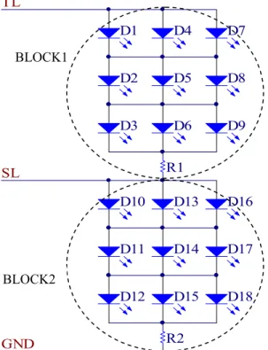
Fig. 4 shows the electronic scheme of a common commercially available LED-based brake light. In Fig. 4, the terminal labeled TL has to be connected to a switch TL to supply a 12-V DC power supply. This switch TL is used to control the turning on and off of the tail lights. The terminal labeled SL has to be connected to a switch SL to supply a 12-V DC power supply. This switch SL controls the operation of the stop light. The current-limiting resistors R1 and R2 control the brightness of Light Emitting Diodes (D3-D11). In Fig. 4, when switch TL is on, resistor R1 limits the magnitude of forward current in the LEDs for normal operation. If switch SL is on, the forward
Figurre 1. Conventional brake lights
Figure 2. Proposed LED-based X-shape brake lights
D1 D2 D3 R1 VCC GND
Figure 3. Rough scheme of conventional brake light current in the LEDs will increase due to the parallel connection of R1 and R2. The lower resistance
increases the brightness of the LEDs. The diodes D1 and D2 are used to ensure the proper direction of conducted current. However, it can be observed that the series connection of LEDs (D3-D5) has larger failure possibility because the current path will be blocked if one of the LEDs fails to work.
D3 D4 D5 D6 D7 D8 D9 D10 D11 R1
TL
SL
GND
R2 D1 D2Figure 4. The common commercially available LED-based brake light scheme
D1 D2 D3 D4 D5 D6 D7 D8 D9 D10 D11 D12 D13 D14 D15 D16 D17 D18 R1 R2 SL TL GND
Figure 5. Proposed circuit scheme
Such a failure results in the elements D3-D5 cannot be lighted up. The D6-D8 and D9-D11 have the same problems [5-6].
BLOCK1
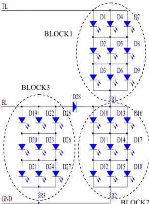
To improve the conventional LED-based brake light design, we propose a high reliability realization circuit, as shown in Fig. 5. It is composed of two similar blocks. In Fig. 5, the terminal labeled TL is connected to a switch TL to supply a 12-V DC power supply. This switch TL is used to control the operation of the tail light. The terminal labeled SL is connected to a switch SL to supply a 12-V DC power supply. The switch SL controls the operation of the stop light. When switch TL is on, the supply voltage conducts the elements in BLOCK1 and BLOCK2 of the circuit in Fig. 5. The resistors R1 can be used to adjust the magnitude of forward current of the LEDs in BLOCK1 and BLOCK2. When switch SL is on, the supply voltage conducts the elements in BLOCK2 with higher current. The LEDs in BLOCK1 are off because the forward-biased voltage is insufficient. Resistors R2 can be used to adjust the magnitude of forward current of the LEDs in BLOCK2 of the proposed brake light. To achieve better warning effect, the LEDs in BLOCK2 can be arranged to light up in X-shape, as shown in Fig. 2. If we intend to light up more LEDs to enhance the warning effect, similar BLOCK and a diode can be jointed. As shown in Fig. 6, the BLOCK3 and D28 have been added. When switch TL is on, the supply voltage conducts the elements in BLOCK1 and BLOCK2. The BLOCK3 will not affect the circuit operation due to the use of D28. It should be noted that the proposed circuit in Figs. 5 and 6 possess better reliability since the series connection of LEDs in Fig. 4 is not adopted in our proposed circuit.
Furthermore, it is known that LED has the property of lower response time. So a flashing signal can be easily realized with LEDs. For the proposed design in Fig. 7, it is arranged that the LEDs flash in X-shape. The 555 timer IC-based astable multivibrator is used to control the flash operation of the brake light. In Fig. 7, when switch TL is on, the supply voltage provides the bias voltage for turning on transistor Q1. Thus all LEDs in the circuit can be lighted up. When switch SL is on, the astable multivibrator output a square wave to turn on and off transistor Q1. So the LEDs (D10-D18) flash with a frequency as the square wave.
3. Experiments
To verify the feasibility of the proposed schemes, the circuits in Figs. 5 and 7 have been implemented, as
D1 D2 D3 D4 D5 D6 D7 D8 D9 R1 D10 D11 D12 D13 D14 D15 D16 D17 D18 R2 D19 D20 D21 D22 D23 D24 D25 D26 D27 R3 D28 TL BL GND
Figure 6. Proposed circuit with enhanced effect
D1 D2 D3 D4 D5 D6 D7 D8 D9 D10 D11 D12 D13 D14 D15 D16 D17 D18 R1 R2 1 2 3 4 5 6 7 8 U1 NE555 R13 R14 R15 R11 R12 C1 Q1 GND SL TL
Figure 7. Proposed circuit with flash function BLOCK3
BLOCK1
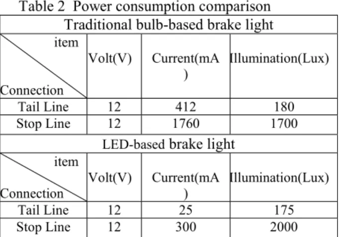
shown in Fig. 8. We compare the power dissipations of our proposed circuit with the traditional bulb-based brake light. The power consumption of the traditional one is more than 5 times the power consumption of the LED-based brake light. The comparison is given in Table 2.
Table 2 Power consumption comparison Traditional bulb-based brake light
item Connection Volt(V) Current(mA ) Illumination(Lux) Tail Line 12 412 180 Stop Line 12 1760 1700
LED-based brake light
item Connection Volt(V) Current(mA ) Illumination(Lux) Tail Line 12 25 175 Stop Line 12 300 2000
Besides, if we use a switch to turn off the 555 timer IC-based astable multivibrator in Fig. 7, its function is the same as the circuit in Fig. 5. Thus the design owns multi-function property. Its workability has been verified.
Figure 8. Practical circuit implementation 4. Conclusion
This project demonstrated that the replacement of a brake light from a traditional incandescent light to LED is achievable. We present a novel vehicle brake light with many advantages. Due to the use of LED light source, the proposed brake light gains the profit of longer useful life, high brightness, low power consumption, less heating, larger mechanic resistance to vibrations and quick response time. The advantages of enhanced warning effect, low cost, high reliability, brightness adjustability, low power consumption and multi-function are attained by circuit design technique, such as simpler structure, using fewer elements and novel design. Practical implementation has been
performed to verify the workability. Thus the objective of traffic safety enhancement is expected.
5. Acknowledgement
This work was supported by the National Science Council of the Republic of China (Grant No. NSC 97-2622-E-151-006-CC3) and BAU-YI Machinery Company. The authors would like to thank system-on-chip (SOC) consortium for printed circuit board fabrication.
6. References
[1] K. Werner, “Higher Visibility for LEDs”, IEEE Spectrum, 39, pp. 30-34, 1994.
[2] D. Gacio, J. Cardesin, E. L. Corominas, J. M. Alonso, M. Dalla-Costa, A. J. Calleja, “Comparison among Power LEDs for Automotive Lighting Applications”, IEEE Industry Applications Society Meeting, pp. 1-5, 2008.
[3] S. B. Peralta and H.E. Ruda, “Applications for Advanced Solid-State Lamps”, IEEE Industry Applications Magazine, pp. 31-42, July/August 1998.
[4] Report of traffic accidents for roadway, National Police Agency, Ministry of the Interior, R.O.C., 2002-2006.
[5] A. V. Ortega and I. N. da Silva, “Technique for Application of Hi-Bright LED in Automobile Industry Through Intelligent Systems”, International Joint Conference on Neural Networks, Volume 3, 12-17 May, pp. 2674-2679, 2002.
[6] W. R. Young, Jr. and W. Wilson, “Efficient Electric Vehicle Lighting Using LEDs”, Southcon. Conference Record, pp.276-280, 1996.