ECS Solid State Letters, 3 (9) R45-R47 (2014) R45 2162-8742/2014/3(9)/R45/3/$31.00©The Electrochemical Society
Crystal Quality and Light Output Power of GaN-Based LEDs
Grown on Nanoporous Patterned Sapphire Substrate
Chien-Chih Chen,aChun-Yan Yap,aWen-Yang Hsu,aCheng-Ta Kuo,bTzong-Liang Tsai,b Jui-Yi Chu,band YewChung Sermon Wua,∗,z
aDepartment of Materials Science and Engineering, National Chiao Tung University, Hsinchu 30010, Taiwan bLextar Electronics Corporation, Hsinchu 30075, Taiwan
The crystal quality and light output power of GaN-based LEDs grown on nanoporous patterned sapphire substrate (NPSS) were investigated. NPSS was prepared using an anodized aluminum oxide (AAO) layer. It was found that the crystal quality of GaN-based LEDs grown on NPSS was better than that on micron-sized patterned sapphire substrate (MPSS) and conventional sapphire substrate. However, the light output power of GaN-based LEDs grown on NPSS was smaller than that on MPSS because the light extraction efficiency (LEE) of MPSS was much larger than that of NPSS.
© 2014 The Electrochemical Society. [DOI:10.1149/2.0021409ssl] All rights reserved.
Manuscript submitted May 14, 2014; revised manuscript received June 6, 2014. Published July 1, 2014.
High-brightness GaN-based light-emitting diodes (LEDs) have been widely used in a variety of applications due to their advantages of high efficiency, long life, small size and environmental protection. Many techniques such as pendeoepitaxy,1epitaxial lateral overgrowth (ELOG)2and patterned sapphire substrate (PSS)3–5have been devel-oped to improve the optoelectronic characteristics of LED. Currently, the PSS technique has attracted much attention because it can improve both internal quantum efficiency (IQE) and light extraction efficiency (LEE).6–8This is because with increase in growth time of GaN, lat-erally grown GaN caused the threading dislocations to bend toward the patterns. Most previous studies indicated that reducing the pattern size to nanoscale can further enhance the optoelectronic character-istics and GaN crystal quality of LED.9,10Nevertheless, the cost of nano-sized PSS was high.
In this study, nano-sized PSS was fabricated using anodic alu-minum oxide (AAO).11,12After growth of the GaN layer, air voids were formed at the GaN/sapphire interface. The crystallinity and the performance of LEDs were investigated.
Experimental
Two-inch c-plane sapphire with 50-nm GaN and 100-nm SiO2on top of the substrate was used in this study. A 2-μm-thick aluminum layer was then deposited on the substrate to fabricate an AAO layer, which was formed by a two-step anodization process at 4◦C. The sample was first anodized in 0.1-M phosphoric acid (H3PO4) under a dc voltage of 140 V for 2000 sec. The AAO film thus formed was subsequently removed by a solution comprising 1.5 wt% Cr2O3and 6 wt% H3PO4mixed at 60◦C for 10 min. The second anodization step was carried out under the same conditions until the entire Al layer was anodized. Then 5 wt% H3PO4was utilized to extend the AAO pore size and remove the barrier layer for 90 min.
The AAO film was used as a dry-etching hard mask. The nano voids were transferred to the SiO2/GaN/sapphire substrate by the high-density plasma reactive ion etching system (HDP-RIE). The etching gases were CHF3(40 sccm) and O2(20 sccm) for oxide, BCl3 (9 sccm) and Cl2 (36 sccm) for GaN, and BCl3 (40 sccm) and Cl2 (10 sccm) for sapphire. The bias, power and pressure were 120 W, 600 W and 10 mTorr, respectively. After the AAO layer was removed, the SiO2layer was removed by a buffer-oxide etching (BOE) solution. The LED structure was grown by low-pressure metallorganic chemical vapor deposition (MOCVD), which was denoted as NPSS. For the purpose of comparison, LED structures were also grown on conventional sapphire substrate (CSS) and cone-shaped micron-sized patterned sapphire substrate (MPSS). The diameter of the micron-sized pattern was 2.5μm, the space was 0.5 μm, and the height was 1.5μm. In this study, the chip had an area of 1 × 1 mm2.
∗Electrochemical Society Active Member. zE-mail:[email protected]
Results and Discussion
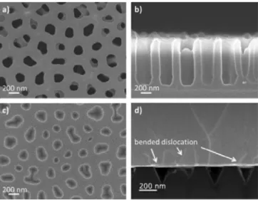
Figure1aand1bshows scanning electron microscope (SEM) im-ages of AAO on SiO2/GaN/sapphire substrate. The diameter and the depth of the nanopores were 150–250 nm and 850 nm, respectively. Figure 1c shows the image of the GaN/sapphire surface after the transfer process. The diameter and the depth of the NPSS voids were 100–200 nm and 260 nm, respectively.
The GaN crystal quality was analyzed by (1) X-ray diffraction (XRD) and (2) reverse leakage current. XRD rocking curves show that the full-width at half-maximum (FWHM) of NPSS was smaller than that of MPSS and CSS, as shown in TableI, indicating that the GaN crystallinity of NPSS was superior to that of MPSS and CSS.
The reverse electrical characteristics of LEDs were measured at a voltage of –5 V. The leakage current of NPSS was 4.7 nA, which was smaller than that of MPSS (13.7nA) and CSS (67.9 nA). Since the reverse leakage current increased with threading dislocation density,8 the GaN crystallinity of NPSS was better than that of MPSS and CSS. Compared with CSS, NPSS and MPSS had better crystallinity due to the patterns on sapphire. For GaN on PSS, with increase in growth time, GaN epilayers on the c-plane sapphire covered these patterns by lateral growth causing the bending of threading dislocations.9,10 More-over, theoretical and experimental studies indicate a further reduction in GaN defect density when the lateral overgrowth approach was re-duced to nanoscale (NPSS).9,10 As a result, NPSS has better GaN quality than the other two LEDs. The bending of NPSS dislocations was shown in Fig.1d.
Figure 1. SEM images of (a) top-view and (b) cross-section of AAO layer on SiO2/GaN/sapphire substrate, and (c) top-view of NPSS substrate. (d) Cross-sectional STEM image of NPSS-LED.
) unless CC License in place (see abstract). ecsdl.org/site/terms_use
address. Redistribution subject to ECS terms of use (see 140.113.38.11
R46 ECS Solid State Letters, 3 (9) R45-R47 (2014)
Table I. Characteristics of LEDs.
FWHM of XRCs Forward
(arcsec) Voltages (V) LOP (mW) Divergent Simulation of
(002) (102) @ 350 mA @ 350 mA Angle (degree) LEE (%)
CSS 533.77 565.42 3.80 252.2 155.1 9.56
MPSS 413.82 417.64 3.79 368.6 143.8 20.99
NPSS 317.34 321.16 3.75 271.1 153.4 12.62
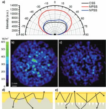
The power-current-voltage (L-I-V) characteristics of LEDs are shown in Fig.2. As listed in TableI, the forward voltage of NPSS at 350 mA was 3.75 V, which was lower than that of MPSS and CSS. Surprisingly, the light output power (LOP) of MPSS LEDs was better than that of NPSS ones, even though the GaN crystal quality of MPSS was not as good as that of NPSS. This observation suggested that the LEE of MPSS must be much higher than that of NPSS. This was confirmed by measuring the radiation patterns of LEDs as shown in Fig.3a. Their divergent angles (half-center brightness, which is the angle for 50% of full luminosity) are summarized in TableI. As can be seen, the divergent angle of MPSS was 143.8◦, which was much smaller than that of NPSS (153.4◦) and CSS (155.1◦). In other words, photons can escape more easily from the MPSS/GaN interface than from the NPSS/GaN and CSS/GaN interfaces.13
The simulation also proves that the LEE of MPSS (20.99%) is higher than that of NPSS (12.62%) and CSS (9.56%), as listed in TableI. The simulation was performed using the Trace-Pro software, as shown in Fig.3band3c. In this simulation, the diameter of the MPSS pattern was 2.5μm, its space was 0.5 μm, and its height was 1.5μm. On the other hand, the diameter of the NPSS void was 200 nm, its space was 200 nm, and its depth was 200 nm. The thickness of sapphire, n-GaN, MQW and p-GaN were 400μm, 2.5 μm, 58 nm and 100 nm, respectively; while their refractive indexes were 1.78, 2.42, 2.54 and 2.45, respectively.14Here, a 200 mW power (5000 light rays) is assumed to emit randomly from the MQW.
As listed in TableI, the LEE of MPSS was 20.99%, which was 1.66 times higher than that of NPSS (12.62%). However, the measured LOP of MPSS were 368.6 mW, which was only 1.35 times higher than that of NPSS. These differences were due to (1) the ignored absorption of metal electrodes and ITO layer in simulation, and (2) the better GaN quality of NPSS compared with that of MPSS.
The detailed analysis of LEE is discussed in the following. The refractive indexes of GaN, sapphire and air are 2.43, 1.78 and 1.00, respectively. According to Snell’s law, light travels from GaN to air only within a critical angle of 24.3◦. The light reaching the surface beyond this angle will experience total internal reflection and will continue to be reflected within the LED until it is absorbed. The critical angle from GaN to sapphire is 47.1◦, while that from sapphire
Figure 2. Power-current-voltage (L-I-V) curves of LEDs.
to air is 34.2◦. This total internal reflection problem can usually be solved by roughening the surfaces/interfaces of LEDs.15–17
As shown in Fig.3d, the cone-shaped interfaces of MPSS not only reflected the downward photons, but also redirected the photons which were originally emitted out of the escape cone, back into the escape cone.
However, there is no cone-shaped interface in NPSS. As seen in Fig.3e, both the GaN/sapphire and GaN/air void interfaces were flat. As a result, lots of the downward photons still suffer from to-tal reflection. There are three reflection paths for downward pho-tons according to their incident angles at the interface. When the incident angle is larger than 47.1◦(critical angle from GaN to sap-phire), the light will experience total internal reflection in GaN until it is absorbed and there is no LEE enhancement. At incident angle smaller than 24.3◦ (critical angle from GaN to air), downward pho-tons are redirected through the GaN/sapphire and GaN/air void inter-faces. Some of these photons will be reflected from the bottom sap-phire/air interface when their redirected angle exceeds the critical an-gle (34.2◦). As these reflected photons pass through the GaN/sapphire and GaN/air void interfaces, they may be redirected back into the escape cone. As a result, LEE is improved. When the incident angle is between 47.1◦ and 24.3◦, downward photons will be reflected at the GaN/air void interfaces but transmitted at the GaN/sapphire in-terfaces. Some of the transmitted photons would behave like photons at incident angle smaller than 24.3◦. Consequently, LEE was also improved.
The analysis results suggested that the LEE of NPSS was larger than that of CSS, but less than that of MPSS.
Figure 3. (a) Radiation patterns of LEDs. (b) and (c) Simulation data of MPSS and NPSS. (d) and (e) Possible photon paths of MPSS and NPSS.
) unless CC License in place (see abstract). ecsdl.org/site/terms_use
address. Redistribution subject to ECS terms of use (see 140.113.38.11
ECS Solid State Letters, 3 (9) R45-R47 (2014) R47
Conclusions
In this study, NPSS was prepared using an AAO film as a dry-etching hard mask. The crystal quality and light output power of NPSS were compared with GaN grown on MPSS and CSS. I-V and XRD analysis revealed that the crystal quality of NPSS was better than that of MPSS and CSS. However, the light output power of NPSS was not as good as that of MPSS. This is because the GaN interface of MPSS was cone-shaped, while that of NPSS was flat. As a result, the LEE of MPSS was much larger than that of NPSS. This LEE difference was confirmed by measuring the LED radiation patterns, optical simulation, and the possible photon paths.
Acknowledgments
This project was funded by Lextar Electronics Corporation and the National Science Council under grant No. 101–2221-E-009–053-MY3. Technical supports from the National Nano Device Laboratory, Center for Nano Science and Technology and Nano Facility Center of the National Chiao Tung University are also acknowledged.
References
1. K. Linthicum, T. Gehrke, D. Thomson, E. Carlson, P. Rajagopal, T. Smith, D. Batchelor, and R. Davis,Appl. Phys. Lett., 75, 196 (1999).
2. A. Sakai, H. Sunakawa, and A. Usui,Appl. Phys. Lett., 71, 2259 (1997). 3. D. S. Wuu, W. K. Wang, K. S. Wen, S. C. Huang, S. H. Lin, R. H. Horng, Y. S. Yu,
and M. H. Pan,J. Electrochem. Soc., 153, G765 (2006).
4. C. H. Chiu, H. H. Yen, C. L. Chao, Z. Y. Li, P. Yu, H. C. Kuo, T. C. Lu, S. C. Wang, K. M. Lau, and S. J. Cheng,Appl. Phys. Lett., 93, 081108 (2008).
5. H. C. Lin, R. S. Lin, J. I. Chyi, and C. M. Lee,IEEE Photonics Technol. Lett., 20, 1621 (2008).
6. Y. J. Lee, T. C. Hsu, H. C. Kuo, S. C. Wang, Y. L. Yang, S. N. Yen, Y. T. Chu, Y. J. Shen, M. H. Hsieh, M. J. Jou, and B. J. Lee,Mater. Sci. Eng., B, 122, 184 (2005).
7. Y. J. Lee, J. M. Hwang, T. C. Hsu, M. H. Hsieh, M. J. Jou, B. J. Lee, T. C. Lu, H. C. Kuo, and S. C. Wang,IEEE Photonics Technol. Lett., 18, 1152 (2006). 8. Y. Cheng, L. Wang, Y. Zhang, H. Zheng, J. Ma, X. Yi, G. Wang, and J. Li,ECS Solid
State Lett., 2, Q93 (2013).
9. H. Gao, F. Yan, Y. Zhang, J. Li, Y. Zeng, and G. Wang,J. Appl. Phys., 103, 014314 (2008).
10. C. Y. Hsieh, B. W. Lin, H. J. Cho, B. M. Wang, and Y. S. Wu,ECS J. Solid State Sci. Technol., 1, Q35 (2012).
11. L. C. Chen, C. K. Wang, J. B. Huang, and L. S. Hong,Nanotechnology, 20, 085303 (2009).
12. Z. J. Tsai, J. K. Liou, and W. C. Liu,IEEE Electron Device Lett., 34, 909 (2013). 13. W. C. Peng and Y. S. Wu,Appl. Phys. Lett., 88, 181117 (2006).
14. T. X. Lee, C. Y. Lin, S. H. Ma, and C. C. Sun,Opt. Express, 13, 4175 (2005). 15. C. Rooman, M. Kuijk, S. De Jonge, and P. Heremans,IEEE Photonics Tech. Lett.,
17, 2649 (2005).
16. Y. C. Lee, C. E. Lee, H. C. Kuo, T. C. Lu, and S. C. Wang,IEEE Photonics Tech. Lett., 20, 369 (2008).
17. L. J. Yan, J. K. Sheu, W. C. Wen, T. F. Liao, M. J. Tsai, and C. S. Chang,IEEE Photonics Tech. Lett., 20, 1724 (2008).
) unless CC License in place (see abstract). ecsdl.org/site/terms_use
address. Redistribution subject to ECS terms of use (see 140.113.38.11