國 立 交 通 大 學
電子工程學系電子研究所碩士班
碩 士 論 文
新穎的金氧半電晶體雜訊模型與
應用於超寬頻系統低雜訊放大器之設計
Novel Noise Modeling of RF MOSFETs and
the Design of an UWB LNA with Modified
L-degenerate Input Matching
研究生: 賴照民
指導教授: 荊鳳德 博士
新穎的金氧半電晶體雜訊模型與
應用於超寬頻系統低雜訊放大器之設計
Novel Noise Modeling of RF MOSFETs and the Design of an
UWB LNA with Modified L-degenerate Input Matching
研 究 生:賴照民 Student:Zhaomin Lai
指導教授:荊鳳德 Advisor:Albert Chin
國 立 交 通 大 學
電子工程學系電子研究所碩士班
碩
士 論 文
A ThesisSubmitted to Department of Electronics Engineering and Institute of Electronics College of Electrical Engineering and Computer Science
National Chiao Tung University in partial Fulfillment of the Requirements
for the Degree of Master of Science in
Electronics Engineering
July 2005
Hsinchu, Taiwan, Republic of China
新穎的金氧半電晶體雜訊模型與
應用於超寬頻系統低雜訊放大器之設計
學生: 賴照民 指導教授: 荊鳳德 博士
國立交通大學
電子工程學系電子研究所
摘要
我們已經發展出新穎的微帶線結構用來直接量得 NFmin 而不需要複雜的校正手續(de-embedding),以取代傳統的 CPW 結構。在 10GHz、0.18μm MOSFET 8 gate
fingers 條件下,非常低的 NFmin,0.9dB,可以直接量測得而不需要任何的校正。 在精準的雜訊量測結果為基準下,我們發展出新穎的金氧半電晶體雜訊模型可以來 預測元件的雜訊表現與特性。此外,我們修改了窄頻低雜訊放大器所使用的源極電感 回授匹配方式,並且將它應用於設計超寬頻低雜訊放大器。該放大器採用台積電 0.18 微米製程,在 3~10GHz 的範圍裡達到輸入與輸出的阻抗匹配並提供 10dB 的功 率增益。在 1.8V 的供應電壓下消耗 27mW 的功率,而第一級放大及僅銷耗 15mW。在 這篇論文中,我們將會說明如何修改源極電感回授匹配及其原理,以及如何將之應 用於超寬頻低雜訊放大器中。
Novel Noise Modeling of RF MOSFETs and the
Design of an UWB LNA with Modified Source
L-degenerate Input Matching
Student: Zhaomin Lai
Advisor: Dr. Albert Chin
Department of Electronics Engineering
And Institute of Electronics
Nation Chiao Tung University
Abstract
A novel micro-strip line layout is developed to direct measure the min. noise figure
(NFmin) accurately instead of the complicated de-embedding procedure in conventional
CPW line. Very low NFmin of 0.9 dB at 10 GHz is directly measured in 8 gate fingers
0.18µm MOSFETs without any de-embedding. Based on the accurate NFmin
measurement, we have developed the novel NFmin model to predict device noise
characteristics. Besides, we also designed an UWB LNA with Modified Source
L-degenerate by using TSMC 0.18µm technology. The LNA provides a forward gain (S21)
of 10dB over the 3 ~ 10 GHz range with a low noise figure of 3.5dB (at 6 GHz) while
consuming 27mW from 1.8V power supply. To achieve its wide-band characteristics, a
novel input matching mechanism is proposed, which modifies L-degenerate approach for
誌謝
本論文得以完成,首先要感謝我的指導老師 荊鳳德 教授,
在兩年的碩士研究生涯裡,給予我豐富的指導與照顧,不論是
研究上與生活裡都讓我在這兩年裡獲得許多的收穫。
另外,我還要感謝黃志翔學長、于殿聖學長與詹歸娣學姊他
們在研究上與學業上給我的幫助,讓我得以順利完成碩士研
究。也要感謝大月、秋峰、櫸壇、阿甫以及實驗室大家,因為
有你們的陪伴與支持,讓我度過愉快又充實的這兩年。
最後,我要對我的父母以及哥哥獻上最高的敬意與謝意,感
謝家人們對我的栽培、支持與鼓勵,才讓我有機會能接觸這一
切並且完成我的學業與研究。
CONTENTS
Chapter 1
Introduction
……….……….. 1
Chapter 2
Thermal Noise in MOSFETs
2.1 Noise Sources in MOSFETs………. 4
2.2 Noise Analysis
2.2.1 Review ……….. 92.2.2 Two-port noise theory ………
10
2.2.3 Further analysis ………..
15
Chapter 3
MOSFETs Noise Coefficients Extraction
3.1 Introduction ………... 22
3.2 Extraction Results ………. 28
3.3 Conclusions ………... 33
Chapter 4
UWB LNA Design
4.1 Introduction ………... 34
4.2 Design Procedures ………. 35
4.3 Simulation Results ………. 37
4.4 Measurements and Conclusions ……… 42
Chapter 5
Summary
……….. 47
Figure Caption
Figure 1 Substrate thermal noise.
Figure 2 Drain induced gate noise.
Figure 3 Equivalent circuits.
Figure 4 Equivalent noise model.
Figure 5 Complex parasitic circuits of CPW layout.
Figure 6 Developed microstrip line structure.
Figure 7(a) NFmin of different fingers on microstrip.
Figure 7(b) NFmin of different fingers on CPW.
Figure 8 Equivalent noise resistance of different fingers versus freq.
Figure 9 Test-key layout.
Figure 10 Γopt of different fingers on smith chart.
Figure 11 Extracted γ factor of different fingers at 10GHz.
Figure 12 Modeling and measured Bopt of different fingers at 10GHz.
Figure 13 Modeling and measured Gopt of different fingers at 10GHz.
Figure14 Modeling and measured NFminof different fingers at 10GHz.
Figure 15 the optimum source impedance versus frequencies of 32 gate fingers.
Figure 16 the NFmin versus frequencies of 32 gate fingers.
Figure 17 Summary of MOSFETs characteristics.
Figure 18 Circuits diagram.
Figure 19 Chip layout.
Figure 20 Simulated S11 & S22.
Figure 22 Simulated NF and NFmin.
Figure 23 Simulated reverse isolation.
Figure 24 Simulated stability.
Figure 25 Two tones test.
Figure 26 Power-out versus power-in.
Figure 27 Simulated circuits SPEC summary.
Figure 28 Measured power gain.
Figure 29 Measured noise figure.
Figure 30 Measured S11 and S22.
Figure 31 Measured S12.
Figure 32 Measured linearity.
Figure 33 Measured results summary.
Figure 34 Die photo.
I.
Introduction
Si RF MOSFETs [1]-[5] are now widely used for wireless communication due to the continuously improved RF noise and high frequency gain with technology downscaling evolution. The increasing operation frequency to higher band with wider bandwidth is the technology trend for communication system. The demand of high performance low noise MOSFET becomes more urgent for ultra-wide band (UWB) (3.1-10.6 GHz) beyond current W-LAN (5.2-5.8 GHz), since the noise also increases monotonically with increasing frequency. However, accurate RF noise modeling of the nm-scale MOSFETs is challenging due to the limited understanding of noise sources and the large parasitic effect from low resistance Si substrate [5]-[7]. Another problem for the nm-scale MOSFET is the large gate resistance where a parallel multiple gate fingers layout is used to reduce the Rg generated thermal noise [5]. Unfortunately, the consumed DC and RF power also increase with increasing finger number that is contradictory to the low power trend.
To accurately model the MOSFETs noise performance, in this paper we first developed a novel micro-strip line layout that can directly measure the NFmin with good accuracy. Very low as-measured NFmin of 0.9 dB is measured at 10 GHz in 8 gate fingers 0.18µm MOSFETs without any de-embedding, where the new micro-strip line design was used to screen out the RF noise generated by the resistance from low
resistance Si substrate. Such low NFmin is comparable with de-embedded 0.13 µm node MOSFETs (80 nm gate length) [3]-[4].
At RF frequencies, the MOSFET 1/f noise becomes negligible and thermal noise is the dominant source of noise. The topic of this paper is about the high frequency thermal noise of RF MOSFETs. Thermal noise is due to the random thermal motion of charge carriers. It not only manifests itself in the drain current noise spectrum, but due to the capacitive coupling between channel and gate, also in the gate current noise spectrum. In the next section, we will analyze the mechanism of the noise sources of MOSFETs, and derive many theoretically equations about the RF MOSFETs noise performance. In the section three, we will extract the important noise coefficients, like the correlation factor c and γ, from our accurate measurement and further develop our noise model of RF MOSFETs. Then, the forth section, is the second major topic about the UWB LNA design. We will represent how to achieve wideband matching by modified the famous source L-degenerate which can make good input matching and also yield nearly optimal noise figure at the response frequency in narrow band LNA. Finally, in the section five, we will summarize a conclusion to our study.
Total 801.11 a/b/g single chip by CMOS.
http://www.atheros.com
UWB applications.
II. Thermal Noise in MOSFETs
2.1 Noise Sources in MOSFETs
(a) Drain Current Noise
There are three main sources which contribute the thermal noise of MOSFETs [8]. And the dominate noise source of RF MOSFETs is the drain current noise which is expressed as:
f
g
KT
i
nd2=
4
γ
d0∆
where gd0 is the drain-source conductance at zero VDS. The coefficient γ has a vale of
unity at zero VDS and, in long channel devices, decrease toward a value of 2/3 in
saturation [9]. Some measurements show that short-channel devices exhibit noise considerably in excess of values predicted by long-channel theory, sometimes by an order of magnitude in extreme cases. Some of the literature attributes this excess noise to carrier heating by the large electric fields commonly encountered in such devices. In this view, the high fields produce carriers with abnormally high energies. No longer in quasi-thermal equilibrium with the lattice, these hot carriers produce abnormal amount of noise. But in contrast to other groups, we find only a moderate enhancement of the drain current noise for short-channel MOSFETs by our good measurements. The details will be illustrated in the section three.
(b) Substrate Thermal Noise
substrate
cbC
subR
drain
source
gate
substrate
cbC
subR
drain
source
gate
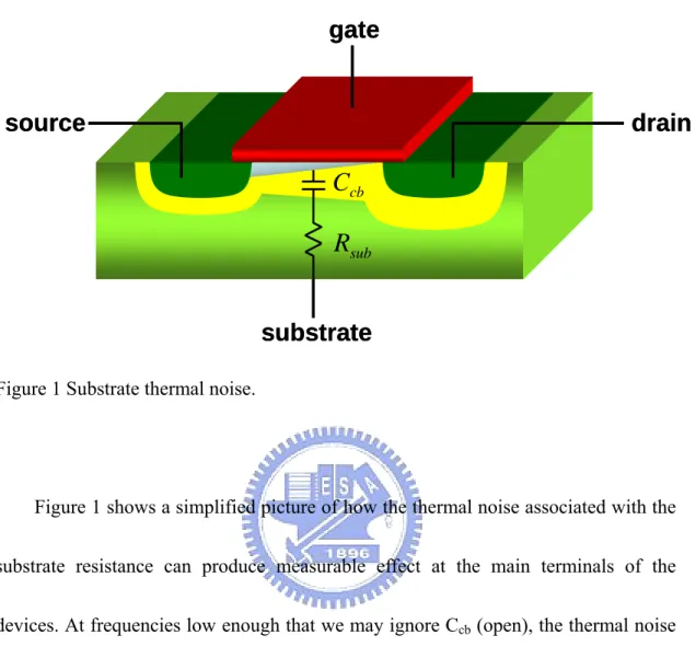
Figure 1 Substrate thermal noise.
Figure 1 shows a simplified picture of how the thermal noise associated with the substrate resistance can produce measurable effect at the main terminals of the devices. At frequencies low enough that we may ignore Ccb (open), the thermal noise
of Rsub modulates the potential of the back gate, contributing some noisy drain
current:
f
g
KTR
i
nd2 ,sub=
4
sub mb2∆
Depending on bias conditions – and also on the magnitude of the effective substrate resistance and size of the back-gate transconductance – the noise generated by this mechanism may actually exceed the thermal noise contribution of the ordinary channel charge. In this regime, layout strategies that reduce the substrate resistance
have a noticeable and beneficial effect on noise.
At frequencies well above the pole formed by Ccb and Rsub, however, the
substrate thermal noise becomes unimportant, as is readily apparent from inspection of the physical structure and the corresponding frequency-dependent expression for the substrate noise contribution [9]:
f
C
R
g
KTR
i
cb sub mb sub sub nd=
+
2∆
2 2 ,)
(
1
4
ω
The characteristics of many IC processes are such that this pole is often around 1 GHz. Excess noise produced by this mechanism consequently will be most noticeable below about 1 GHz.
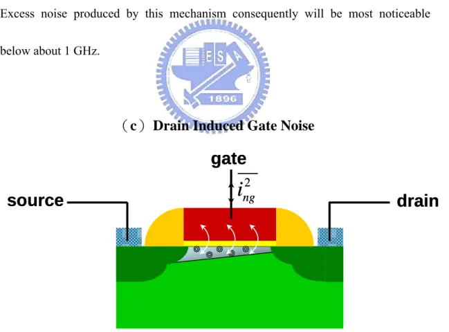
(c) Drain Induced Gate Noise
2 ng
i
drain
source
gate
2 ngi
drain
source
gate
2 ng
i
g
gC
gs 2 ngi
g
gC
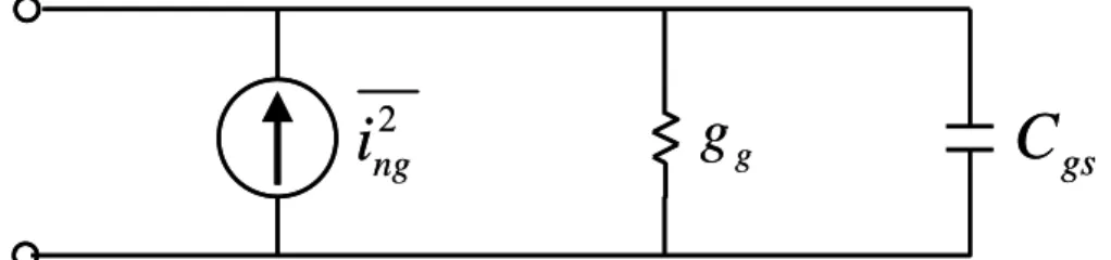
gsFigure 3 Equivalent circuits.
In addition to drain noise, the thermal agitation of channel charge has another important consequence: gate noise. The fluctuating channel potential couples capacitively into the gate terminal, leading to a noisy gate current (see figure 2). Noisy gate current may also be produced by thermally noisy resistive gate material. But this noise source will be separately discussed later, even though it is more and more important in nano-scale devices. Although the drain-induced-gate-noise is negligible at low frequencies, it can dominate at radio frequencies. Van der Ziel has shown that the drain-induced-gate-noise may be expressed as:
f
g
KT
i
ng2=
4
δ
g∆
where the parameter gg is:0 2 2
5
d gs gg
C
g
=
ω
Van der Ziel gives a value of 4/3 (twice γ) for the gate noise coefficient, δ, in long channel devices [9].
The circuit model for the drain-induced-gate-noise is a conductance connected between gate and source, shunted by a noise current source (see figure 3). This noise current clearly has a spectral density that is not constant. In fact, it increases with frequency, so perhaps it ought to be called “blue noise” to continue the optical analogy. Because the drain thermal current noise and the drain-induced-gate-noise do share a common origin, they are correlated. That is, there is a component of the gate noise current that is proportional to the drain noise current on an instantaneous basis.
Although the noise behavior of long-channel devices is fairly well understood, the precise behavior of δ and γ in the short-channel regime is still unknown at present. That’s why we have to do more research on the thermal noise of MOSFETs. Thermal noise of deep sub-micrometer MOSFETs has received considerable attention lately, which is mainly triggered by publications that report a severe enhancement of the thermal noise with respect to long-channel theory [10]–[14]. In the earliest of these publications [10], thermal noise was found to be enhanced by a factor up to 12 in n-channel devices with 0.7µm gate length and hot electrons were proposed to explain these results. Evidently, the reported noise enhancements would seriously limit the viability of RF CMOS and a detailed study is called for. Therefore, in this paper, we perform an extensive study of the RF noise in 0.18µm RF CMOS technology.
2.2 Noise Analysis
2.2.1 Review
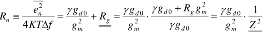
To analyze the relationship between noise performance and the characteristics of MOSFETs, we have derived the NFmin based on the intrinsic MOSFETs with additional Rg and following the procedure in reference [3]:
⎟⎟
⎠
⎞
⎜⎜
⎝
⎛
+
≅
+
+
=
∆
g m g ox f m iR
g
kT
kTR
f
WLC
K
g
kT
f
v
γ
γ
4
4
1
4
2 (1) m gs D m m gs G ig
C
kT
f
I
K
g
kT
g
C
qI
f
i
ω
γ
ω
2 2γ
2 2 2 24
4
2
⎟⎟
≅
⎠
⎞
⎜⎜
⎝
⎛
+
+
=
∆
(2)⎟⎟
⎠
⎞
⎜⎜
⎝
⎛
+
⎟⎟
⎠
⎞
⎜⎜
⎝
⎛
+
+
=
∆
+
∆
+
=
m gs s g m S s i S ig
C
R
R
g
R
f
R
kT
i
f
kTR
v
NF
γ
ω
2 2γ
2 21
1
1
4
4
1
(3) 2 2 2 ) ( i i opt si
v
R
=
(4)γ
γ
γ
γ
π
1
2
1
/
4
1
2 min m g t g m m gsR
g
f
f
R
g
g
C
f
NF
≈
+
+
⋅
=
+
+
(5)In above equations, the 1/f terms are neglected due to high RF frequency. The γ is the proportional constant of the drain current noise, which was previously attributed to hot electron effect in short channels. The derived NFmin in equation (5) has exactly the same dependence of f, Cgs and gm with Fukui’s experimental equation [15] for GaAs FETs that suggests the good accuracy of the derived equation.
But the noise equations which we derive just before still have some loss and unreasonable parts. Those are the “lacking of drain-induced-gate-noise” and the “wrong optimized source impedance - Yopt”. We did not account the
drain-induced-gate-noise in the noise sources. And the Yopt is also incorrect since it
has merely the real part, which is inconsistent with usual measurements. We will fix the bugs and further enhance the accuracy of our noise equations, but we need to do more study on noise theory, two-port noise theory at first.
2.2.2 Two-port noise theory
The noise factor is defined as:
source
input
to
due
noise
output
power
noise
output
total
F
≡
(6)The noise factor is a measure of the degradation in signal-to-noise ratio that a system introduces. The larger the degradation, the larger the noise factor. If a system adds no noise of its own then the total output noise is due entirely to the source, and the noise factor is therefore unity.
s
Y
- +
si
ne
ni
Noiseless
2-port
sY
- +
si
ne
ni
Noiseless
2-port
In the model of figure 4, all of the noise appears as input to the noiseless network, so we may compute the noise figure there. A calculation based directly on Eqn. 6 requires the computation of the total power due to all of the sources, and dividing that result by the power due to the input source. An equivalent and simpler method is to compute the total short-circuit mean-square noise current and then divide that total by the short-circuit mean-square noise current due to the input source. This alternative method is equivalent because the individual power contributions are proportional to the short-circuit mean-square current, with a proportionality constant (which involves the current division ratio between the source and two-port) that is the same for all the terms.
In carrying out this computation, one generally encounters the problem of combining noise sources that have varying degree of correlation with one another. In the special case of zero correlation, the individual powers superpose. For example, if we assume, as seems reasonable, that the noise powers of the source and of the two-port are
Uncorrelated, then the expression for noise figure becomes [8]:
2 2 2 s n s n s
i
e
Y
i
i
F
=
+
+
(7)two-port’s generators are also uncorrelated with each other.
In order to accommodate the possibility of correlations between en and in,
express in as the sum of two components. One, ic, is correlated with en, and the other,
iu, isn’t:
u c
n
i
i
i
=
+
(8)Since ic is correlated with en, it may be treated as proportional to it through a constant
whose dimensions are those of an admittance:
n c c
Y
e
i
=
(9)The constant Yc is known as the correlation admittance. Combining Eqn. 7, 8, and 9,
the noise factor becomes:
2 2 2 2 2 2 2
1
)
(
s n s c u s n s c u si
e
Y
Y
i
i
e
Y
Y
i
i
F
=
+
+
+
=
+
+
+
(10)The expression in Eqn. 10 contain three independent noise sources, each of which may be treated as thermal noise produced by an equivalent resistance or conductance (whether or not such a resistance or conductance actually is the source of the noise):
f
KT
e
R
n n≡
4
∆
2 (11)f
KT
i
G
u u≡
4
∆
2 (12)f
KT
i
G
s s≡
4
∆
2 (13)Using these equivalences, the expression for noise factor can be written purely in terms of impedances and admittances:
s n s c s c u s n s c u
G
R
B
B
G
G
G
G
R
Y
Y
G
F
]
)
(
)
[(
1
1
2 2 2+
+
+
+
+
=
+
+
+
=
(14)where we have explicitly decomposed each admittance into a sum of a conductance G and a susceptance B.
once a given two-port’s noise has been characterized with its four noise parameters (Gc, Bc, Rn, and Gu), Eqn. 14 allows us to identify the general conditions
for minimizing the noise factor. Taking the first derivative with the respect to the source admittance and setting it equal to zero yield:
opt c s
B
B
B
=
−
=
(15) opt c n u sG
G
R
G
G
=
+
2=
(16)Hence, to minimize the noise factor, the source susceptance should be made to equal to the inverse of the correlation susceptance, while the source conductance shoule be set equal to the value in Eqn. 16.
⎥
⎦
⎤
⎢
⎣
⎡
+
+
+
=
+
+
=
c c n u n c opt nG
G
R
G
R
G
G
R
F
min1
2
(
)
1
2
2 (17)Thus, contours of constant noise factor are non-overlapping circles in the admittance plane.
It is important to recognize that, although minimizing the noise factor has something of the flavor of maximizing power transfer, the source admittance leading to these condition are generally not the same – as is apparent by inspection of Eqn. 15 and 16. For example, there is no reason to expect the correlation susceptance to equal to the input susceptance (except by coincidence). As a consequence, one must generally accept less than maximum power gain if noise performance is to be optimized, and vice versa.
2.2.3 Further analysis
Now, we start to derive the new noise equations of the relationship between noise performance and the characteristics again. Recall that the MOSFETs noise model consists of two generators. The mean-square drain current noise from the thermal current noise and the substrate thermal noise is:
f
C
R
g
KTR
f
g
KT
i
cb sub mb sub d nd∆
+
+
∆
=
0 2 2 2)
(
1
4
4
ω
γ
(18)We will ignore the second term of the drain thermal current noise since it will drop quickly at the high frequencies range.
The drain-induced-gate-noise is:
f
g
KT
i
ng2=
4
δ
g∆
(19) where 0 2 25
d gs gg
C
g
=
ω
(20)Further recall that the drain-induced-gate-noise is correlated with the drain noise, with a correlation coefficient defined formally as:
2 2 nd ng nd ng
i
i
i
i
c
⋅
⋅
≡
∗ (21)The long-channel value of c is theoretically –j0.395. Precise measurements of the correlation coefficient are difficulty to carry out (especially in the deep sub-micron
factor of 2 of this theoretically value, even for devices with drawn channel lengths as small as 0.13µm.
To derive the four equivalent two-port noise parameters, repeated here for convenience,
f
KT
e
R
n n≡
4
∆
2 (11)f
KT
i
G
u u≡
4
∆
2 (12) c c n c cG
jB
e
i
Y
≡
=
+
(22)We first reflect the two fundamental MOSFETs noise source back to the input as a different pair of equivalent input generator (one voltage and one current source).
The equivalent input noise voltage generator accounts for the output noise observed when the input port is short-circuited. To determine its value, reflect the drain current noise back to the input as a noise voltage source and recognize that the ratio of these quantities is simply gm. But there is one more important noise source
which should be added in account. That is the gate resistance thermal noise which becomes more and more significant effect on the noise performance in recently deep sub-micron technology. Thus, the over all equivalent input noise voltage generator including gate resistance and the reflected noise current is equal to:
0 2 0 2 2 2 2 2
4
d m g d m nd g m nd ng
g
R
g
g
i
f
KTR
g
i
e
γ
γ
+
⋅
=
∆
+
=
(23)from which it is apparent that equivalent input noise voltage is completely correlated, and in phase, with the drain current noise. Thus, we can immediately determine the equivalent noise resistance that:
0 2 0 2 0 2 0 2
4
d m g d m d g m d n ng
g
R
g
g
g
R
g
g
f
KT
e
R
γ
γ
γ
γ
+
⋅
=
+
=
∆
≡
(24)The equivalent input noise voltage generator by itself does not fully account foe the drain current noise, however, because a nosy drain current also flows even when the input is open-circuits and the drain-induced-gate-noise is ignored. Under this open-circuit condition, dividing the drain current noise by the transconductance yields an equivalent input which, when multiplied by the input admittance, gives us the value of an equivalent input current noise that completes the modeling of ind:
2 0 0 2 2 2 2 2 2 1
(
)
)
(
m g d d gs n m gs nd ng
R
g
g
C
j
e
g
C
j
i
i
+
⋅
=
=
γ
γ
ω
ω
(25)In this step of the derivation, we have assumed that the input impedance of a MOSFET is purely capacitive. This assumption is a good approximation for frequencies well below ωT, if appropriate high-frequency layout practice is observed
to minimize gate resistance. Given this assumption, Eqn. 25 shows that the input noise current in1 is in quadrature, and therefore completely correlated, with the equivalent
The total equivalent input current noise is the sum of the reflected drain noise contribution of Eqn. 25 and the induced gate current noise. The induced gate noise current itself consists of two terms. One, which we’ll denote ingc, is fully correlated
with the drain current noise, while the other, ingu, is completely uncorrelated with the
drain current noise. Hence, we may express the correlation admittance as follows:
⎟⎟
⎠
⎞
⎜⎜
⎝
⎛
⋅
+
⋅
=
⋅
+
+
+
=
+
+
=
+
=
+
=
≡
nd ngc m gs nd ngc d m g d m m g d d gs n ngc m g d d gs n ngc n c c n c ci
i
g
C
j
Z
i
i
g
g
R
g
g
g
R
g
g
C
j
e
i
g
R
g
g
C
j
e
i
i
jB
G
e
i
Y
ω
γ
γ
γ
γ
ω
γ
γ
ω
0 2 0 2 0 0 2 0 0 1 (26)For simplifying the expression, we define a gate-resistance coefficient, Z, with the following relation: 2 0 0 m g d d
g
R
g
g
Z
+
=
γ
γ
(27)So we can redraw some of the formulas which we just derived before as:
2 2 2 0 2 0 2 2 2 2 2
4
1
Z
g
i
g
g
R
g
g
i
f
KTR
g
i
e
m nd d m g d m nd g m nd n=
⋅
+
⋅
=
∆
+
=
γ
γ
(28) 2 2 2 2 0 0 2 2 2 2 2 2 1(
)
(
)
)
(
Z
C
j
e
g
R
g
g
C
j
e
g
C
j
i
i
n gs m g d d gs n m gs nd n=
⋅
+
⋅
=
=
ω
γ
γ
ω
ω
(29)2 2 0 0 2 0 2 0 2 0 2
1
4
g
Z
g
g
g
R
g
g
g
R
g
g
f
KT
e
R
m d d m g d m d g m d n n=
⋅
+
⋅
=
+
=
∆
≡
γ
γ
γ
γ
γ
(30)To express Yc in a more useful form, we need to incorporate the induced gate
noise correlation factor explicitly. To do so, we must manipulate the last term of Eqn. 26 in ways that will initially appear mysterious. First, we express it in terms of cross-correlations by multiplying both numerator and denominator by the conjugate of the drain noise current and then averaging each:
gs d m nd ng m nd ng ng nd nd ng m nd nd ng m nd nd nd ngc m nd ngc m
C
c
g
g
i
i
c
g
i
i
i
i
i
i
g
i
i
i
g
i
i
i
i
g
i
i
g
ω
λ
δ
⋅
⋅
=
⋅
=
⋅
⋅
=
⋅
⋅
=
⋅
⋅
⋅
=
⋅
∗ ∗ ∗ ∗5
0 2 2 2 2 2 2 2 (31)If we assume that c continues to be purely imaginary, even in the short-channel regime, we finally obtain a useful expression for the correlation admittance by combining Eqn. 26 and 31 as that:
⎟⎟
⎠
⎞
⎜⎜
⎝
⎛
−
=
⎟⎟
⎠
⎞
⎜⎜
⎝
⎛
⋅
+
⋅
=
γ
δ
α
ω
ω
5
1
c
C
Z
j
i
i
g
C
j
Z
Y
gs nd ngc m gs c (32)where we have used the substitution:
0 d m
g
g
=
α
(33)Since α is unity for long-channel devices and progressively decrease as channel lengths shrink, it is one measure of the departure from the long-channel regime.
We see from Eqn. 32 that the correlation admittance is purely imaginary, so that Gc=0. more significant, however, is the fact that Yc does not equal the admittance of
Cgs, although it is some multiple of it. Hence, one cannot maximize power transfer
and minimize noise figure simultaneously. To investigate further the important implications of this impossibility, though, we need to derive the last remaining noise parameter, Gu.
Using the definition of the correlation coefficient, we may express the induced gate noise as follows:
)
1
(
4
4
)
(
2 2 2 2c
g
f
KT
c
g
f
KT
i
i
i
ng=
ngc+
ngu=
∆
δ
g+
∆
δ
g−
(34) The last term in Eqn. 34is uncorrelated portion of the induced gate noise current, so that, finally: 0 2 2 2 2 25
)
1
(
4
)
1
(
4
4
d gs g u ug
c
C
f
KT
c
g
f
KT
f
KT
i
G
=
−
∆
−
∆
=
∆
≡
δ
δω
(35)With these parameters, we can determine both the source impedance that minimizes the noise figure as well as the minimum noise figure itself:
⎟⎟
⎠
⎞
⎜⎜
⎝
⎛
−
−
=
−
=
γ
δ
α
ω
5
1
c
C
Z
B
B
opt c gs (36)From Eqn. 36, we see that the optimum source susceptance is essentially inductive in character, except that it has the wrong frequency behavior. Hence, achieving a broadband noise matching is fundamentally difficult.
Continuing, the real part of the optimum source admittance is:
)
1
(
5
2 2c
C
Z
G
R
G
G
c gs n u opt=
+
=
γ
−
δ
αω
(37)And the minimum noise figure is given by:
)
1
(
5
2
1
)
1
(
5
2
1
)
(
2
1
2 2 minc
Z
c
g
Z
C
G
G
R
F
T m gs c opt n−
+
≈
−
+
=
+
+
=
δ
γ
ω
ω
δ
γ
ω
(38)In Eqn. 38, the approximation is exact if one threats ωT as simply the ratio of gm
to Cgs. Note that if there were no the drain-induced-gate-noise current (i.e., if δ were
zero), the minimum noise figure would be 0 dB. That unrealistic prediction along should be enough to suspect that the induced gate noise must indeed exist. Also note that, in principle, increasing the correlation between drain and gate current noise would improve noise figure, although correlation coefficient unrealistic near unity would be required to effect large reductions in noise figure.
Another important observation is that improvements in ωT that accompany
technology scaling also improve the noise figure at any given frequency. However, the rapid pace of change in IC technology virtually guarantees an incomplete understanding of the behavior of transistors of the most recent generations of technology. Because the detailed behavior of some of the coefficients in the short-channel regime is still unknown, we will have to make accurate noise
measurement and then carefully extract the important MOSFETs noise coefficients.
III. MOSFETs Noise Coefficients Extraction
3.1 Introduction
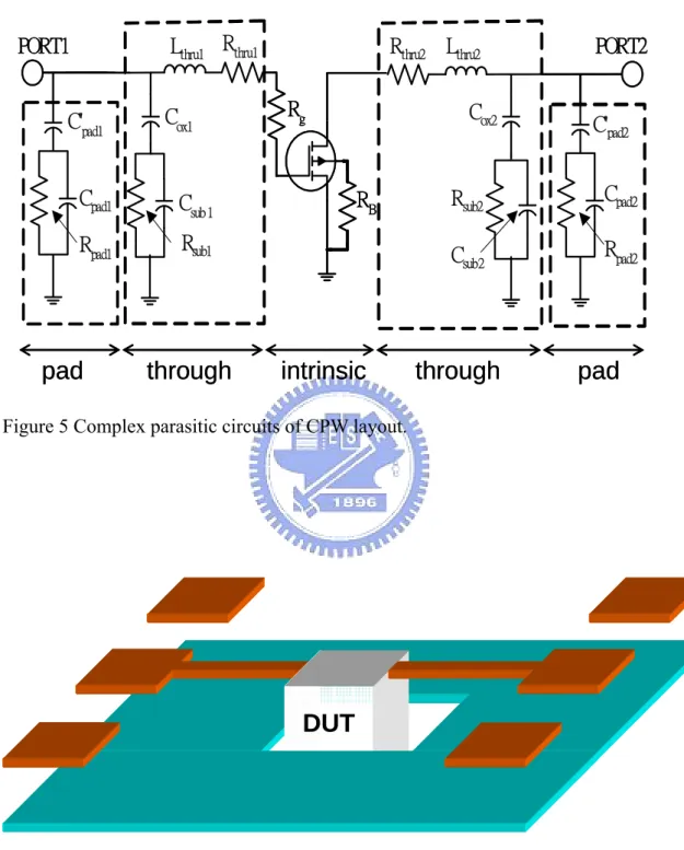
The RF noise is difficult to measure in Si MOSFETs due to the strong parasitic substrate loss (shown in fig. 5) that dominates the noise in as-measured NFmin. De-embedding is required to give the much smaller intrinsic NFmin [3]-[5] - this can produce errors. To overcome this problem we used a novel microstrip transmission line layout, which is shown in figure 6. Figures 7(a) and 7(b) show the as-measured NFmin of different gate fingers devices, respectively. The as-measured NFmin using the standard CPW transmission line design is also shown for comparison. A large NFmin reduction over the whole frequency range is observed using the microstrip line design, even without de-embedding. At 10 GHz, the as-measured NFmin is only 0.9 dB for the 8 gate-finger MOSFET. This is the lowest reported NFmin for a 0.18 µm MOSFET and is comparable with the data for 0.13 µm devices (Lg= 80nm) [4]-[5]. The low NFmin of 0.9 dB at 10 GHz is sufficient for UWB (3.1-10.6 GHz) applications.
Figure 5 Complex parasitic circuits of CPW layout.
DUT
DUT
Figure 6 Developed microstrip line structure. Lthru1 Csub1 Rsub1 Rthru2 Lthru2 PORT1 PORT2 Csub2 Rsub2 RB Rthru1 Rg Cox1 Cox2 Rpad1 Cpad1 C'pad1 Rpad2 Cpad2 C'pad2
pad through intrinsic through pad
Lthru1 Csub1 Rsub1 Rthru2 Lthru2 PORT1 PORT2 Csub2 Rsub2 RB Rthru1 Rg Cox1 Cox2 Rpad1 Cpad1 C'pad1 Rpad2 Cpad2 C'pad2
0 2 4 6 8 10 12 14 16 18 20 0.0 0.5 1.0 1.5 2.0 2.5 NFmin_Micr ostr ip ( d B ) Frequency 8 fingers 16 fingers 32 fingers 64 fingers
Figure 7(a) NFmin of different fingers on microstrip.
0 2 4 6 8 10 12 14 16 18 20 0 1 2 3 4 5 6 NF mi n _ CPW (d B) Frequency 8 fingers 16 fingers 32 fingers 64 fingers
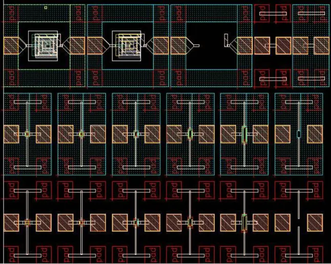
The equivalent noise resistance of the two-port, which is shown in figure 8, decreases slightly with increasing frequencies. This is because that the substrate thermal noise which we ignore in our noise equations contributes some the equivalent noise resistance. As a result, we will extract the noise coefficients, such as γ and δ, at high frequencies range (10GHz) in order to get the better accuracy.
0 2 4 6 8 10 12 14 16 18 20 0 50 100 150 200 250 300 350 400 Rn Frequency 8 fingers 16 fingers 32 fingers 64 fingers
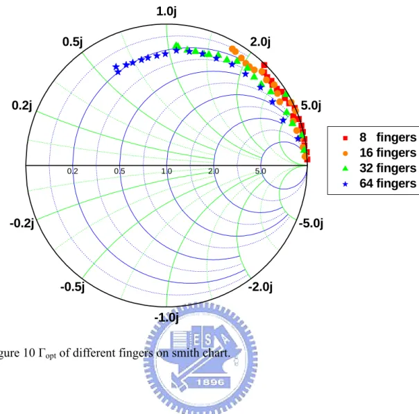
0.2 0.5 1.0 2.0 5.0 -0.2j 0.2j -0.5j 0.5j -1.0j 1.0j -2.0j 2.0j -5.0j 5.0j 8 fingers 16 fingers 32 fingers 64 fingers
Figure 10 Γopt of different fingers on smith chart.
The figure 9 is the layout of the ultra-low noise MOSFETs, which includes the conventional CPW and our microstrip layout of MOSFETs and two more 3D inductors. And the figure 10 shows the optimum source impedance of the ultra-low noise MOSFETs. Sine we have derived the accurate noise data, we will start to extract the noise coefficients in the next step.
3.2 Extraction Results
According to our noise equations, we can extract the thermal drain current noise factor, γ, from Rn which is shown in the equation 30.
2 2 0 0 2 0 2 0 2 0 2
1
4
g
Z
g
g
g
R
g
g
g
R
g
g
f
KT
e
R
m d d m g d m d g m d n n=
⋅
+
⋅
=
+
=
∆
≡
γ
γ
γ
γ
γ
(30)By our extraction, the thermal drain current noise factor, γ, is about to 0.9, which is shown in figure 11. In contrast to some other groups, we find only a moderate enhancement of the drain current noise for short channel MOSFETs. The abnormal among of noise from other group’s results maybe due to inaccuracy measurements, lacking of gate and substrate thermal noise, or inappropriate layout.
0 10 20 30 40 50 60 70 0.0 0.2 0.4 0.6 0.8 1.0 1.2 γ fac tor Fingers Number gama γ=2/3
The other two coefficients, c and δ, can be extract from equation 36~38 which are recalled again here for convenience.
⎟⎟
⎠
⎞
⎜⎜
⎝
⎛
−
−
=
−
=
γ
δ
α
ω
5
1
c
C
Z
B
B
opt c gs (36))
1
(
5
2 2c
C
Z
G
R
G
G
c gs n u opt=
+
=
γ
−
δ
αω
(37))
1
(
5
2
1
)
1
(
5
2
1
)
(
2
1
2 2 minc
Z
c
g
Z
C
G
G
R
F
T m gs c opt n−
+
≈
−
+
=
+
+
=
δ
γ
ω
ω
δ
γ
ω
(38)By the extraction, the correlation factor, c, remains the value of –j0.395 as it in the long-channel regime theory [9], while δ is twice the value of γ. This value of δ is reasonable since it comes from the thermal drain current noise.
Figure 12 ~ 17 show the extraction results. Figure 12 and 13 represent the measured and modeling optimum source impedance respectively at 10GHz, while figure 14 is the measured and modeling NFmin at 10GHz. And figure 15 demonstrate the measured and modeling optimum source versus frequencies with 32 gate fingers, while figure 16 is the measured and modeling NFmin versus frequencies with 32 gate fingers. Very Good agreement between the measurements and our modeling is achieved by using our derived noise equations. Figure 17 tabulates the relative characteristics of the RF MOSFETs that we measured.
0 10 20 30 40 50 60 70 -0.016 -0.014 -0.012 -0.010 -0.008 -0.006 -0.004 -0.002 0.000 B opt Fingers Number modeling data measured data
Figure 12 Modeling and measured Bopt of different fingers at 10GHz.
0 10 20 30 40 50 60 70 0.000 0.001 0.002 0.003 0.004 0.005 0.006 G opt Fingers Number modeling data measured data
0 10 20 30 40 50 60 70 0.0 0.5 1.0 1.5 2.0 NF mi n (d B) Fingers Number modeling data measured data
Figure14 Modeling and measured NFminof different fingers at 10GHz.
0 1 1 2 5 -0j 0j -1j 1j -1j 1j -2j 2j -5j 5j measured modeling
0 2 4 6 8 10 12 14 16 18 0.0 0.5 1.0 1.5 2.0 2.5 NF min (d B) Frequencies modeling data measured data
Figure 16 the NFmin versus frequencies of 32 gate fingers.
2γ 2γ 2γ 2γ δ j0.395 j0.395 j0.395 j0.395 c 48.5 49 49 49 ft (GHz) 0.968404 0.971626 0.973147 0.973859 Z 0.919952 0.906415 0.886442 0.876605 γ 1.9 3.45 6.55 12.74 Rg (Ω) 30.55 61.67 123.62 246.91 Rn (Ω) 0.433333 0.397163 0.380497 0.375849 α 0.171 0.0987 0.0523 0.0265 gdo (A/V) 0.0741 0.0392 0.0199 0.00996 gm (A/V) 64 32 16 8 Characteristics
\
F.N. 2γ 2γ 2γ 2γ δ j0.395 j0.395 j0.395 j0.395 c 48.5 49 49 49 ft (GHz) 0.968404 0.971626 0.973147 0.973859 Z 0.919952 0.906415 0.886442 0.876605 γ 1.9 3.45 6.55 12.74 Rg (Ω) 30.55 61.67 123.62 246.91 Rn (Ω) 0.433333 0.397163 0.380497 0.375849 α 0.171 0.0987 0.0523 0.0265 gdo (A/V) 0.0741 0.0392 0.0199 0.00996 gm (A/V) 64 32 16 8 Characteristics\
F.N.3.3 Conclusions
We have developed a new microstrip line design to measure NFmin accurately without the need for complicated de-embedding. Based on the accurate NFmin measurement and analytical NFmin equation, close agreements to the measurements with modeling data are all obtained that is important for further circuit application.
IV. UWB LNA Design
4.1 Introduction
Ultra wideband (UWB) systems are a new wireless technology capable of transmitting data over a wide spectrum of frequency bands with very low power and high data rates. Among the possible applications, UWB technology may be used for imaging systems, vehicular and ground penetrating radars, and communication systems. Although the UWB standard (IEEE 802.15.3a [16]) has not been completely defined, most of the proposed applications are allowed to transmit in a band between 3.1 and 10.6 GHz. In this work, the design of a low noise amplifier (LNA) in a 0.18µm CMOS technology for the receiver path of a UWB system is discussed. Such an amplifier must feature wide-band input matching to a 50Ω antenna, flat gain over the entire bandwidth, good linearity, minimum possible noise figure and low power consumption.
In recent years, narrow-band CMOS LNA designs have employed inductive source degeneration to achieve good input matching. This technique also yields nearly optimal noise figure at the resonance frequency of the input network [17]. In the proposed wide-band design in Figure 16 (at the next section), the inductively degenerated common source topology is further explored. The input impedance Zin is embedded in a two-section band-pass filter to resonate its reactive part over the whole
band. The cascode configuration improves the reverse isolation and the frequency response of the amplifier. Source-follower buffer of the second stage is intended for measurement purposes, i.e. to drive an external 50Ω load.
4.2 Design Procedures
In this work, we first use inductive source degeneration to achieve good matching to 100Ω in stead of the conventional 50Ω to decrease the Q value of the serial resonance circuits. This is because that the lower Q value implies the wider bandwidth, which makes a broadband matching. Then we add an L-section circuit to transfer the 100Ω to the source impedance 50Ω. Finally by using CAD tool to optimize the circuits, we can achieve an input reflection coefficient to smaller than -10dB in-band: Ls=0.9nH, Lg=1.6nH, L1=0.9nH and C1=0.25pF. The size of M1 is chosen as 128 gate fingers to minimize the inductance values. The bias of M1 is set for balance between gain and power consumption.
The cascode device is chosen as small as possible to reduce the parasitic capacitances. A lower limit to the width of M2 (24 gate fingers) is set by its reasonable Vds. Both M1 and M2 are minimum length devices. The load is designed to achieve flat gain over the whole bandwidth. In-band, M1 acts as a current amplifier, the input current being Vin/Rs, and the current gain β(ω)=gm/(jωCgs). To compensate
for the roll-off of β(ω), a shunt-peaked load is used. The value of the inductance L2 (2.3nH) is limited by acceptable power gain over shooting. Resistance RL (60Ω)
improves the gain at lower frequency. All the design and the layout are shown in figure 18 and figure 19 respectively.
M1 M2 M3 M4 Ls Lg L1 C1 RL L2 L3 M1 M2 M3 M4 Ls Lg L1 C1 RL L2 L3
Figure 19 Chip layout.
4.3 Simulation results
Figure 20 shows the simulated input and output reflection coefficients. S11 is lower than -8dB between 3.1 and 12GHz. The output buffer achieves excellent matching such that S22 is lower than -10dB from 1.7GHz to 15.9 GHz. Figure 21 is the power gain versus frequencies, and the maximum power gain is 10.4dB in our simulation results. Since the output source follower drives a matched load, the voltage gain of the core amplifier is exactly 6dB higher than S21. The -3dB bandwidth is 0.4~9.9GHz for the simulation. The noise figure (NF) of this UWB LNA is shown in Figure 22. The noise figure is as low as 3.3dB at 6GHz which is the center frequency
of UWB system, while the average noise figure in-band is about 4dB. Figure 23 and 24 show the simulated reverse isolation S12 and stability factor respectively. The two-tone test results for third-order intermodulation distortion are shown in Figure 25. The test is performed at 6GHz. IIP3 is to 3.3dBm, and the input referred 1-dB compression point (ICP) is -9dBm. These results imply excellent linearity of our LNA. The proposed UWB LNA dissipate 27mW (15mW for first stage) with a power supply of 1.8V. Figure 27 summarizes the performance of the presented amplifiers,
m2
freq=
dB(S(1,1))=-7.956
3.100GHz
m3
freq=
dB(S(1,1))=-8.178
7.900GHz
m4
freq=
dB(S(1,1))=-13.067
10.60GHz
2 4 6 8 10 12 14 16 18 0 20 -20 -15 -10 -5 -25 0 freq, GHz d B (S (1 ,1 ))m2
m3
m4
d B (S (2 ,2 ))m1
freq=
dB(S(2,1))=7.884
3.600GHz
m5
freq=
dB(S(2,1))=10.427
7.500GHz
2 4 6 8 10 12 14 16 18 0 20 0 10 -10 20 freq, GHz d B (S(2 ,1 ))m1
m5
Figure 21 Simulated power gain.
m6
freq=
nf(2)=3.326
6.100GHz
2 4 6 8 10 12 14 16 18 0 20 5 10 15 20 0 25 freq, GHz nf (2 )m6
NF m in2 4 6 8 10 12 14 16 18 0 20 -100 -80 -60 -40 -120 -20 freq, GHz d B (S(1 ,2 ))
Figure 23 Simulated reverse isolation.
2 4 6 8 10 12 14 16 18 0 20 2 3 4 5 1 6 freq, GHz Mu 1 Mu P rime 1
Figure 25 Two tones test.
Figure 26 Power-out versus power-in.
m1
Pin=
dBm(out[::,1])=-0.044
-9.000
-70 -60 -50 -40 -30 -20 -10 0 -80 10 -60 -40 -20 0 -80 20 Pin d B m (o u t[::,1 ])m1
m1 indep(m1)=plot_vs(dBm(out), freq)=-70.1116.000E9 m2
indep(m2)=
plot_vs(dBm(out), freq)=-236.7515.950E9
5.6 5.7 5.8 5.9 6.0 6.1 6.2 6.3 6.4 5.5 6.5 -300 -250 -200 -150 -100 -350 -50 freq, GHz dB m (out ) m1 m2
EqnIIP3=(m1-m2)/2-80 indep(IIP3) <invalid>
IIP3 3.320
27; 15
< -12
< -8
<6
10.4
2~10
P
DC(mW)
S22
(dB)
S11
(dB)
NF
(dB)
Gain
(dB)
B.W.
(GHz)
27; 15
< -12
< -8
<6
10.4
2~10
P
DC(mW)
S22
(dB)
S11
(dB)
NF
(dB)
Gain
(dB)
B.W.
(GHz)
Figure 27 Simulated circuits SPEC summary.
4.4 Measurements and Conclusions
The following figures 28~33 are the measurement results which are only slightly different form our simulation, which imply good accuracy of our simulation and good circuit design. The some of the bandwidth compression showing in figure 28 maybe due to the underestimate of the load resistor parasitic.
0 2 4 6 8 10 12 14 16 -10 -5 0 5 10 15 20 Gain (dB ) Frequencies Figure 28 Measured power gain.
0 1 2 3 4 5 6 7 8 9 10 0 5 10 15 20 NO is e F ig u re (d B) Frequencies Figure 29 Measured noise figure.
0 2 4 6 8 10 12 14 16 -20 -15 -10 -5 0 S11 S22 S-p a rameter s (d B) Frequencies Figure 30 Measured S11 and S22.
0 2 4 6 8 10 12 14 16 -50 -40 -30 -20 -10 0 S12 S-p a rameter s (d B) Frequencies Figure 31 Measured S12. -30 -25 -20 -15 -10 -5 0 -80 -70 -60 -50 -40 -30 -20 -10 0 10 OP1 OP3 Output Powe r (dB ) Input Power (dB) Figure 32 Measured linearity.
Figure 33 Measured results summary.
The bandwidth of this work with considering matching and power gain is from 3 to 8 GHz, while the average power gain is about 8dB which can be up to 14 dB without the current buffer in real cases. The noise performance is good and the minimum noise figure is only 3.5dB at 3~4GHz. The noise figure can be even better if we solve the bandwidth compression problem from the resistor parasitic. Input and output matching are achieved well in band and the linearity of this work is excellent. Total power consumption is 27mW, while the core LNA consumes only 15mW by 1.8V power supply. By the new input matching approach we proposed, a low noise, broadband, low power consumption and good-linearity amplifier is developed for the UWB system applications.
+2
IIP3
(dBm)
27; 15
< -9
< -7
3.5~8
8 (+6)
3~8
P
DC(mW)
S22
(dB)
S11
(dB)
NF
(dB)
Gain
(dB)
B.W.
(GHz)
+2
IIP3
(dBm)
27; 15
< -9
< -7
3.5~8
8 (+6)
3~8
P
DC(mW)
S22
(dB)
S11
(dB)
NF
(dB)
Gain
(dB)
B.W.
(GHz)
Figure 34 Die photo.
Figure 35 Comparison of broadband LNA performance.
2004 0.18μm CMOS 9* -6.7 < -20 < -9.9 4~9 9.3 (+6) 2.4~9.5 [18] 2003 0.18μm CMOS 52 -< -9 < -8 4.3~6 8.1 0.6~22 [19] This work Ref. 27; 15* PDC (mW) 0.18μm CMOS Tech. 2005 year +2 IIP3 (dBm) < -9 < -7 3.5~8 8 (+6) 3~8 S22 (dB) S11 (dB) NF (dB) Gain (dB) B.W. (GHz) 2004 0.18μm CMOS 9* -6.7 < -20 < -9.9 4~9 9.3 (+6) 2.4~9.5 [18] 2003 0.18μm CMOS 52 -< -9 < -8 4.3~6 8.1 0.6~22 [19] This work Ref. 27; 15* PDC (mW) 0.18μm CMOS Tech. 2005 year +2 IIP3 (dBm) < -9 < -7 3.5~8 8 (+6) 3~8 S22 (dB) S11 (dB) NF (dB) Gain (dB) B.W. (GHz)
V. Summary
Let us summary the conclusions of this paper briefly.
Noise modeling: The low noise amplifier in a RF receiver is a significant component, since it plays an important role in the noise performance of a RF system, which affects the dynamic range and the signal to noise ratio of this system. The current noise model with BSIM3v3 core can not model the noise behavior correctly. In order to develop the accurate noise model of RF MOSFETs, we have developed a new microstrip line design to measure NFmin accurately without the need for complicated de-embedding. Based on the accurate NFmin measurement and analytical NFmin equation, close agreements to the measurements with modeling data are all obtained that is important for further circuit application.
UWB LNA: By the new input matching approach we proposed, a low noise, broadband, low power consumption and good-linearity amplifier is developed for the future UWB system applications. The advantages of this design include extending the famous source L-degenerate matching to broadband, low noise, low power consumption, reducing inductor numbers and excellent linearity. All the advantages are important for UWB system considerations.
Reference
[1] Q. Li, J. Zhang, W. Li, J. S. Yuan, Y. Chen, and A. S. Oates, “RF Circuit performance degradation due to soft breakdown and hot carrier effect in 0.18µm CMOS technology,” IEEE RF IC Symp. Dig, pp. 139-142., June 2001.
[2] K. Kuhn, R. Basco, D. Becher, M. Hattendorf, P. Packan, I. Post, P. Vandervoom and I. Young, “A comparison of state-of-the art NMOS and SiGe HBT devices for analog/mixed-signal/RF circuit applications,” Symp. On VLSI Tech., pp. 224-225, June 2004.
[3] M.C. King, Z. M. Lai, C. H. Huang, C. F. Lee, M. W. Ma, C. M. Huang, Y. Chang and Albert Chin, “Modeling finger number dependence on RF noise to 10 GHz in 0.13µm node MOSFETs with 80nm gate length,” IEEE RF IC Symp. Dig., 2004, pp. 171-174.
[4] M. C. King, M. T. Yang, C. W. Kuo, Y. Chang, and A. Chin, “RF noise scaling trend of MOSFETs from 0.5µm to 0.13µm technology nodes,” IEEE MTT-S Int. Microwave Symp. Dig., pp. 6-11, 2004.
[5] C. H. Huang, K. T. Chan, C. Y. Chen, A. Chin, G. W. Huang, C. Tseng, V. Liang, J. K. Chen, and S. C. Chien, “The minimum noise figure and mechanism as scaling RF MOSFETs from 0.18 to 0.13µm technology nodes,” IEEE RFIC Symp., pp. 373-376, 2003.
[6] K. T. Chan, A. Chin, S. P. McAlister, C. Y. Chang, V. Liang, J. K. Chen, S. C. Chien, D. S. Duh, and W. J. Lin, “Low RF loss and noise of transmission lines on Si substrates using an improved ion implantation process,” in IEEE MTT-S International Microwave Symp. Dig., vol. 2, pp. 963-966, 2003.
[7] A. Chin, K. T. Chan, H. C. Huang, C. Chen, V. Liang, J. K. Chen, S. C. Chien, S. W. Sun, D. S. Duh, W. J. Lin, C. Zhu, M.-F. Li, S. P. McAlister and D. L. Kwong, “RF Passive Devices on Si with Excellent Performance Close to Ideal Devices Designed by Electro-Magnetic Simulation,” in International Electron Devices Meeting (IEDM) Tech. Dig., pp. 375-378, 2003.
[8] T. H. Lee, “The Design of CMOS Radio-Frequency Integrated Circuits,”. Cambridge University Press,1998.
[9] A. van der Ziel, Noise in Solid State Devices and Circuits, Wiley, New York, 1986.
[10] A. A. Abidi, “High-frequency noise measurements on FET’s with small dimensions,” IEEE Trans. Electron Devices, vol. ED-33, pp. 1801–1805, 1986.
[11] P. Klein, “An analytical thermal noise model of deep submicron MOSFET’s for circuit simulation with emphasis on the BSIM3v3 SPICE model,” in Proc. 28th Eur. Solid-State Device Research Conf. (ESSDERC), 1998, pp. 460–463.
[12] Klein, P. “An analytical thermal noise model of deep submicron MOSFET’s,” IEEE Electron Device Lett., vol. 20, pp. 399–401, 1999.
[13] G. Knoblinger, “RF noise of deep-submicron MOSFETs: extraction and modeling,” in Proc. 31th Eur. Solid-State Device Research Conf. (ESSDERC), 2001, pp. 331–334.
[14] L. M. Franca-Neto and J. S. Harris, “Excess noise in sub-micron silicon FET: Characterization, prediction and control,” in Proc. 29th Eur. Solid-State Device Research Conf. (ESSDERC), 1999, pp. 252–255.
[15] G. D. Vendelin, A. M. Pavio, and U. L. Rohde, “Microwave circuit design using linear and nonlinear techniques,” John Wiley & Sons, p. 140, 1990 Edition.
[16] http://www.ieee802.org/15/pub/TG3a.html
[17] T. H. Lee, “The Design of CMOS Radio-Frequency Integrated Circuits,”. Cambridge University Press,1998.
[18] A. Bevilacqua and A. M. Niknejad, “An ultra-wideband CMOS LNA for 3.1 to 10.6 GHz wireless receiver,” in IEEE ISSCC Dig. Tech. Papers, 2004, pp. 382–383.
[19] R.-C. Liu, K.-L. Deng, and H.Wang, “A 0.6–22 GHz broadband CMOS distributed amplifier,” in Proc. IEEE Radio Frequency Integrated Circuits (RFIC) Symp., June 8–10, 2003, pp. 103–106.
學經歷
姓名:賴照民 性別:男 出生年月日:民國七十年四月一日 籍貫:台北市 學歷:台北市立建國高中 (85 年 9 月~88 年 6 月) 國立交通大學電子工程學系 (88 年 9 月~92 年 6 月) 國立交通大學電子工程所 (92 年 9 月~94 年 6 月) 論文題目: 新穎的金氧半電晶體雜訊模型與應用於超寬頻系統低雜訊放大器之設計Novel Noise Modeling of RF MOSFETs and the Design of an UWB LNA with Modified L-degenerate Input Matching