國立交通大學
電子工程學系 電子研究所碩士班
碩 士 論 文
應用於超寬頻系統之
低功率、高線性度射頻接收器
Low Power and High Linearity RF Receiver
Circuit for Ultra Wideband System Application
研究生:賴俊豪
指導教授:郭建男 教授
應用於超寬頻系統之低功率、高線性度射頻接收器
Low Power and High Linearity RF Receiver Circuit for
Ultra Wideband System Applicatio
n
研究生: 賴俊豪 Student: Chuan-Hao Lai
指導教授: 郭建男 Advisor: Chien-Nan Kuo
國立交通大學
電子工程學系 電子研究所碩士班
碩士論文
A Thesis
Submitted to Department of Electronics of Engineering & Institute of Electronics College of Electrical Engineering and Computer Engineering
National Chiao Tung University In Partial Fulfillment of the Requirements
For the Degree of Master
In
Electronic Engineering August 2009
Hsinchu, Taiwan, Republic of China
I
應用於超寬頻系統之
低功率、高線性度射頻接收器
學生 : 賴俊豪 指導教授 : 郭建男 教授
國立交通大學
電子工程學系 電子研究所碩士班
摘要
本篇論文利用到複數轉導分析方法,對電晶體提出轉導等效小訊號電路模型, 藉由此分析方法應用於多閘級電晶體架構之線性度分析,相較於之前所提出的分 析方法,在此複數轉導分析下可以提供寬頻的線性度提升特性,以利於改善寬頻 放大器電路之線性度。根據此種分析方法,超寬頻放大器與前端接收電路分別經 由晶片製作來驗證。 第一顆晶片應用於超寬頻系統之-5dBm 之輸入第三階交會點超寬頻放大器 利用到複數導數相消技術。量測結果顯示此一超寬頻放大器在線性度方面具有 5dBm 以上的提升,同時不用消耗多餘的功率。這顆超寬頻放大器在 8.26mW 功 率損秏下,具有8.1dB 之轉換增益,8dB 之輸入反迴損秏以及-5dBm 以上之輸入 第三階交會點。 在第二顆晶片中,設計一個應用於超寬頻系統之低功率、高線性度前端接收 端電路,此接收器電路包含了一個低雜訊放大器,一個主動相位分離器以及一個 直接降頻混頻器。 模擬結果顯示此前端電路有 20.3dB 的轉換增益,10dB 之輸 入反迴損秏以及-4.7dBm 之輸入第三階交會點,此外,此電路消秏功率為 10.4mW。II
Low Power and High Linearity RF Receiver
Circuit for Ultra Wideband System Application
Student : Chuao-Hao Lai Advisor : Chien-Nan Kuo
Department of Electronics Engineering & Institute of
Electronics
National Chiao-Tung University
ABSTRACT
A compact equivalent circuit using a complex transconductance analysis is proposed for linearity design in the multiple gated transistors configuration. This complex transconductance analysis gives broadband linearity improvement in the common source amplifier as compared to previous published analysis. Following the complex transconductance analysis, an UWB LNA and an UWB RF front-end circuit were verified through two individual chips.
In the first chip, -5dBm IIP3 UWB low noise amplifier using complex derivative cancellation technique is analyzed and designed for ultra-wideband system. Measurement results show that the improvement of the linearity is more than 5dB without extra power consumption, and the designed LNA has conversion gain of 8.1dB, input return loss of 8dB, and input third-order intercept point (IIP3) of -5dBm with 8.26mW power dissipation.
In the second chip, a low power and high linearity UWB receiver intends to use in the receiver path of the ultra-wideband system. This front-end circuit is composed of a low noise amplifier, an active balun, and a direct down-conversion mixer. Simulation results show that the circuit has conversion gain of 20.3dB, input return loss of 10dB, IIP3 of -4.7dBm, while consuming only 10.4mW.
III
誌謝
能夠完成畢業論文,順利取得碩士學位,要感謝的人真的很多。首先是,我 的父母親,能夠提供我一個沒有經濟負擔的環境一路往上念。再來,我要對我的 指導教授郭建男教授至上誠摯的感謝。這兩年來,不僅提供了良好的研究環境與 設備,並且讓我對射頻及類比電路的領域有深層的了解。適時的指點迷津,讓我 學習到有邏輯的分析方法與嚴謹的研究態度。此外我要對昶綜,明清和鴻源三位 學長致上萬分的謝意,除了教導我許多軟體與硬體上的使用,也時常分享寶貴的 研究與人生經驗,讓我一直有學習的好榜樣。 感謝實驗室的其他學長姐,鈞琳、俊興、燕霖、煥昇、易耕等的不吝指教與 技術支援。感謝一起奮鬥一起研究的同學子超跟建忠,以及博一、根生、佑緯、 勁夫、敬修、馳光、宇航等學弟,你們使實驗室不再是一個無聊的地方。 最後感謝女朋友惠中一路研究所的陪伴,謝謝你在這一年碩士生活中陪伴我 走過許多人生的起起伏伏。在我研究上遇到瓶頸時,你的鼓勵與支持讓我走過種 種一切的不如意。在我忙碌於研究時,你總是默默的陪伴在我身邊替我加油,讓 我能無後顧之憂的向成功邁進。 賴俊豪 九十八年 八月IV
CONTENTS
Abstract (Chinese)………..I
Abstract (English)……….II
Acknowledgemen……….………III
Contents………IV
Table Captions………...VIII
Figure Captions………XI
Chapter 1 Introduction……….1
1.1 Ultra-Wideband Communication System………...1
1.2 Motivation………...2
1.3 Thesis Organization………3
Chapter 2 Basic Concepts in RF Circuit………..4
2.1 Receiver Architecture………...4
2.1.1 Heterodyne Receiver………4
2.1.2 Homodyne Receiver……….5
2.2 Noise Basic………...6
2.2.1 Noise source……….7
2.2.2 Noise model of MOSFET………8
2.2.3 Noise figure of cascade stage……….10
2.2.4 Noise Factor of a Two Port Network………..10
2.2.5 Optimum Source Impedance for Noise Design………..11
2.3 Linearity and Nonlinearity………..12
V
2.4.1 Harmonic Generation……….13
2.4.2 Intermodulation Distortion……….14
2.5 Fundamental of the Volterra Series……….15
2.6 Nonlinear Performance Parameters in Terms of Volterra
Kernels………17
Chapter 3 General Consideration in RF Circuit Design…..21
3.1 Low Noise Amplifier Basic………21
3.1.1 Low Noise Amplifier Architecture Analysis………..21
3.1.2 Optimizations of Low Noise Amplifier Design Flow………24
3.1.3 Amplifier stability………..26
3.2 Down Conversion Mixer Basic………...28
3.2.1 Conversion gain………..29
3.2.2 Switching stage………..29
3.2.3 Mixer noise……….30
3.2.4 Port to Port isolation………...31
3.2.5 Linearity……….31
Chapter 4 -5dBm IIP3 UWB Low Noise Amplifier Using
Complex Derivative Cancellation Technique………32
4.1 Introduction……….32
4.2 UWB LNA Design Consideration………..……33
4.3 Dual Reactive Feedback Technique For Broadband Input
Impedance Matching………...34
4.3.1 The proposed dual reactive feedback circuit………..34
4.3.2 Gain response……….37
VI
4.4 A 3~11GHz Ultra-Wideband Low Noise Amplifier…………...40
4.5 Analysis of Linearity………..41
4.5.1 Nonlinear effect of common source amplifier………...42
4.5.2 Multiple gate transistors method using complex transconductance analysis……….47
4.5.3 Broadband linearity improvement using MGTR………51
4.6 CMOS Constant Current Reference………...55
4.7 Chip Implementation And Measured Result………...58
4.8 Summary……….62
Chapter 5 A Low Power, High Linearity UWB Receiver for
Ultra-Wide Band Wireless System……….63
5.1 Introduction……….63
5.2 Principle of the Mixer Circuit Design……….65
5.2.1 Transconductance stage………..65
5.2.2 Mixing stage………...69
5.2.3 Current injection mrthod………70
5.3 UWB receiver Simulation Results and Comparison…………...71
5.4 Chip Implementation And Measurement Considerations……...76
5.4.1 Chip Implementation………..76
5.4.2 Measurement Considerations……….76
5.5 Summary……….77
Chapter 6 Conclusion and Future Work………...78
6.1 Conclusion………78
VII
References…...80
Vita………83
VIII
FIGURE CAPTIONS
Fig. 1.1 Multiband spectrum allocation………..1
Fig. 2.1 Simple heterodyne architecture………..5
Fig. 2.2 Rejection of image versus suppression of interferers………5
Fig. 2.3 Simple homodyne receiver architecture………6
Fig. 2.4 A standard noise model of MOSFET………...10
Fig. 2.5 Schematic representation of a system characterized by a Volterra series…16 Fig. 2.6 (a) Growth of output components in an intermodulation test………..20
(b) Intermodulation distortion………..20
Fig. 3.1 Common source input stage with inductive source degeneration…………21
Fig. 3.2 Equivalent noise model of Figure 3.1………..23
Fig. 3.3 Stability of two-port networks embedded between source and load……...27
Fig. 3.4 The simplified CMOS Gilbert Cell mixer………...28
Fig. 4.1 Dual reactive feedback structure………..34
Fig. 4.2 Equivalent circuit of Zopt*………...34
Fig. 4.3 Input impedance changed among the two feedbacks with frequency……..35
Fig. 4.4 Gain response design of the dual reactive feedback stage………...38
Fig. 4.5 (a)The inductive source degeneration feedback can be substituted by the transformer feedback………...38
(b)Their equivalent circuit for input impedance………...38
Fig. 4.6 The dual reactive feedback amplifier with transformer feedback…………39
Fig. 4.7 A 3–11GHz UWB LNA as a design example of dual reactive feedback….41 Fig. 4.8 Gain response………...41
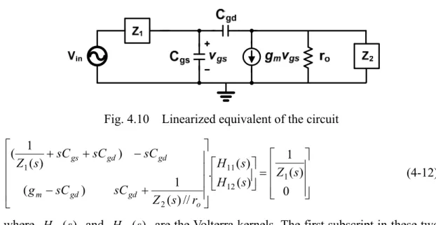
Fig. 4.9 The equivalent circuit of the common-source amplifier………..43
IX
Fig. 4.11 The equivalent circuit for the computation of the second-order………..45
Fig. 4.12 The equivalent circuit for the computation of the third-order kernels….46 Fig. 4.13 MGTR architecture………..48
Fig. 4.14 The compact box-type equivalent circuit model………..48
Fig. 4.15 Cancellation of complex AC gm” in polar plot………..50
Fig. 4.16 Cancellation of AC gm” in MGTR configuration……….50
Fig. 4.17 Search for the optimal device size and bias voltage using IIP3 contour..51
Fig. 4.18 The third order intermodulation of MT and AT in broadband condition.52 Fig. 4.19 Search for the optimal bias voltage using IIP3 contour in broadband condition………...53
Fig. 4.20 The UWB LNA IIP3 be improved in broadband condition……….54
Fig. 4.21 The MGTR cancellation effect in broadband condition………..54
Fig. 4.22 CMOS constant current reference………55
Fig. 4.23 Chip micrograph of the UWB LNA……….58
Fig. 4.24 Measured input impedance matching S11……….59
Fig. 4.25 Measured output impedance matching S22………...60
Fig. 4.26 Measured S12………61
Fig. 4.27 Measured power gain S21……….61
Fig. 4.28 Measured noise figure………..61
Fig. 4.29 IIP3 measurement of w/i MGTR and w/o MGTR broadband LNA……62
Fig. 5.1 UWB receiver front-end architecture……….63
Fig. 5.2 The active balun mixer………...64
Fig. 5.3 The schematic of the broadband down conversion mixer circuit………..65
Fig. 5.4 Common-gate common-source transconductance stage………66
Fig. 5.5 Common-gate common-source transconductance stage………67
X
(b) small signal model of common source……….67
Fig. 5.6 Simulation result of gain error………...69
Fig. 5.7 Simulation result of phase difference……….69
Fig. 5.8 Mixing stage………...70
Fig. 5.9 UWB receiver architecture……….72
Fig. 5.10 CMOS constant current reference………..72
Fig. 5.11 The simulation of input return loss S11……….73
Fig. 5.12 The simulation of conversion gain……….73
Fig. 5.13 The simulation of IIP3………...74
Fig. 5.14 The FOM of UWB receiver performance………..75
Fig. 5.15 Chip layout of UWB receiver front-end circuit……….75
XI
TABLE CAPTIONS
Table 2.1 Different responses at the output of a nonlinear system described by Volterra kernels………...18 Table 4.1 Measured performance summary………..………59 Table 5.1 Summary of performance and comparison………74
1
Chapter 1
Introduction
1.1 Ultra-Wideband Communication System
Ultra-wideband (UWB) is a wireless personal area network technology that transmits a low signal power over a very wide bandwidth and has the promising ability to provide high data rate at low cost with low power consumption. The Federal Communication Commission (FCC) has allocated 7.5GHz of spectrum for unlicensed use of UWB applications in the 3.1 to 10.6GHz frequency band. The multi-band UWB has greater flexibility in coexisting with other international wireless systems and future government regulators, and could avoid transmitting in already occupied bands. The multi-band OFDM based UWB, with fourteen 500MHz sub-bands and a frequency hopping scheme, is the possible approach to meet the requirements of IEEE 802.15.3a standard. Each of these bands must have a bandwidth greater than 500 MHz to obey the FCC definition of UWB. Fig. 1.1 shows the division of UWB frequency spectrum.
2
1.2 Motivation
As introduced in Section 1.1, UWB is becoming more attractive for low cost consumer communication applications and that allows overlying existing narrowband systems to result in a much efficient use of the available spectrum. Thus, UWB is developed to provide a specification for a low complexity, low cost, low power consumption, and high data rate wireless connectivity among device within or entering the personal operating space and also addressed the quality of service capabilities required to support multimedia data types.
The direct down-conversion receiver becomes more attractive since it has the advantages of low complexity, low power, and less extra components. And it lets system-on-chip become possible. Typical, the first stage of the receiver is a low noise amplifier (LNA), which provides high gain and low noise to suppress the overall system’s noise performance. Because LNA is dominating the linearity of the direct down-conversion receiver, we need high linearity to avoid the distortion of the signal. How to improve the linearity of the UWB LNA without extra power consumption is the main object of this thesis.
In the first one for UWB system application, the UWB LNA provides high gain, broadband input matching using dual reactive feedback topology, and broadband linearity improvement using multiple gated transistors (MGTR) technology. For MGTR analysis, we use a complex transconductance analysis for broadband linearity improvement design in this configuration. To design the UWB LNA with low power consumption using multiple gated transistors technology for broadband linearity improvement is the critical challenge for design.
In the second one for UWB system application, a low-power front-end circuit which includes a LNA, an active balun, and the Gilbert cell mixer is designed. The
3
LNA provides high gain and low noise to suppress the overall system’s noise performance. The active balun provides broadband differential output signal for mixer. The double balance Gilbert cell mixer has an acceptable linearity for the receiver. To design an active balun for broadband differential output balance is critical challenge for design.
1.3 Thesis Organization
In the chapter 2 of the thesis, some basic concepts of RF design are introduced. These basic concepts which include the introduction of receiver architecture, noise and linearity provide the guidance for RF circuit design.
In the chapter 3 of the thesis, the design consideration of some circuit blocks which include LNA and mixer is introduced. Based on these circuits, a mixer and a front-end circuit are designed and verified in later chapter.
In the chapter 4 of the thesis, -5dBm IIP3 UWB LNA using complex derivative cancellation technique are designed. The multiple gated transistors configuration is introduced and a compact equivalent circuit using a complex transconductance is proposed for broadband linearity improvement design in this configuration. Following the above analysis, a low-power and high-linearity UWB LNA is designed. Finally, measurement result of the LNA chip fabricated by TSMC 0.18um CMOS technology is discussed.
In the chapter 5 of the thesis, a low-power, high linearity UWB front-end circuit is designed. The first stage is the LNA which is the same as that in chapter 4. The second stage is the active balun which provides the signal into differential form. The last stage is the double balance Gilbert cell mixer which has an acceptable linearity for the receiver. Overall front-end circuit is implemented.
4
Chapter 2
Basic Concepts in RF Circuit
2.1 Receiver Architecture
2.1.1
Heterodyne Receiver
A simple heterodyne architecture is shown in Fig. 2.1. This architecture is the
most reliable reception technique today. But if the cost, complexity, integration and power dissipation are the primary criteria, the heterodyne receiver will become unsuitable due to its complexity and the need for a large number of external components.
In heterodyne architectures, the signal band is translated into much lower frequencies by a down-conversion mixer, and the filters are used to select the band and channel of interest. In general, a low noise amplifier is placed in front of the down-conversion mixer to suppress the noise of the down-conversion mixer.
Frequency planning is important in the heterodyne receiver. For high-side injection, an undesired signal (image) at the frequency of ωIM=ωLO+(ωLO-ωRF) is translated into the same intermediate frequency (IF) as the desired signal. Similarly, for low-side injection, the image frequency is at ωIM=ωLO-(ωLO-ωRF). Therefore the image would cause extra noise at the intermediate frequency. As shown in Fig. 2.2, some techniques are necessary to suppress the image, such as image reject filter. But
here comes the question: how to choose the intermediate frequency? If 2ωIF is
sufficiently large, the rejection of a image filter will have a relatively small loss in the signal band and a large attenuation in the image band. But a lower 2ωIF will relax the quality factor of the channel select filter to get great suppression of nearby interferers. Therefore a trade-off between image rejection and channel selection must be taken.
5
2.1.2
Homodyne Receiver
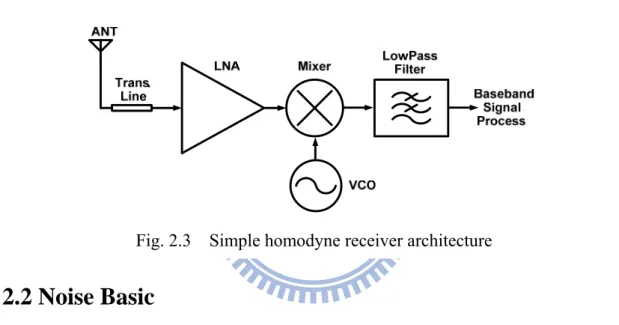
The homodyne receiver is also called “direct-conversion” or “zero-IF” architecture, since the RF signal is directly down-converted to the baseband in the first down conversion. In the homodyne receiver, the LO frequency is equal to the input carrier frequency, and channel selection requires only a low-pass filter with relatively sharp cutoff characteristics. The simple homodyne architecture is shown in Fig. 2.3. However, quadrature outputs are needed for frequency and phase-modulated signals, since the two sides of FM or QPSK spectra carry different information.
In recent years, this architecture becomes the topic of active research gradually and it may be due to the following reasons:
Fig. 2.1 Simple heterodyne architecture
Fig. 2.2 Rejection of image versus suppression of interferers (a) large ω (b) small IF ω IF
6
(1) The problem of image is removed due to ωIF = 0. Therefore no image filter is
required, and the LNA need not drive a 50-Ω load.
(2) It is attractive for monolithic integration because this architecture needs less external components.
For the above reasons, this architecture is suitable for low-power and single-chip design. But some other issues that do not exist or are not as serious in a heterodyne receiver must be entailed, such as channel selection, DC offset, I/Q mismatch, even-order distortion, and flicker noise.
2.2 Noise Basic
Noise can be generally defined as any random interference unrelating to the signal of interest, and it is characterized by a PDF and a PSD. In analog circuits, the signal-to-noise ratio (SNR), defined as the ratio of the signal power to the total noise power, is an important parameter. But in RF design, most of the front-end receiver blocks are characterized in terms of their noise figure, which is a measure of SNR degradation resulting from the added noise from the circuit/system but rather than the input-referred noise. Noise factor can be expressed as following:
Total output noise power Noise Factor
Output noise power due to input source
= (2-1)
7
The noise figure (NF) is simply the noise factor expressed in decibels. If there is no noise in the system, then noise figure is 0 dB regardless of the gain. In reality, the finite noise of a system degrades the SNR, yielding noise figure > 0 dB. For those whose noise factor is close to unity, noise temperature (TN) is an alternative way to
express the effect of noise contribution. Noise temperature is the description of the noise performance in higher-resolution, and is defined as the required temperature increment for the source resistance. Noise temperature is calculated by all of the output noise at the reference temperature Tref (which is 290 K). It relates to the noise
factor as following:
N
N ref ref
T
Noise Factor 1 T T (Noise Factor-1) T
= + ⇒ = ⋅ (2-2)
2.2.1
Noise Source
Thermal noise:
Thermally agitated charge carriers in a conductor constitute a randomly varying current that gives rise to a random voltage resulting from the Brownian motion. Thermal noise is often called Johnson noise or Nyquist noise. The noise voltage has averaged value of zero, but a nonzero mean-square value.
In a resistor R, thermal noise can be represented by a series of noise voltage
source 2 4
n
v = kTR fΔ or by a shunt noise current source 2 4
n kT f i R Δ = , where k is
Boltzmann’s constant (about 1.38×10⁻²³ J/K), T is the absolute temperature in Kelvins,
and Δf is the noise bandwidth. However, purely reactive elements generate no thermal noise.
Shot Noise:
Shot noise occurs in PN junctions, and there occurred two conditions for shot noise:
8
(2) There must be energy barrier over which a charge carrier hops.
Charge comes in discrete bundles. The randomness of the arrival time gives rise to the whiteness of shot noise. Therefore the shot noise can be modeled by a shunt
noise current source 2 2
n DC
i = qI Δf , where q is the electronic charge, IDC is the DC
current in amperes, and Δf is the noise bandwidth in hertz. Flicker Noise:
Flicker noise appears as 1/f character and is found in all active devices, as well as in some discrete passive element such as carbon resistors. In diodes, flicker noise is caused by traps associated with contamination and crystal defects in the depletion regions. The traps capture and release carriers in a random fashion and the time constants associated with the process giving rise to the 1/f nature of the noise power density. The flicker noise in diode can be represented as 2
j j K I i f f A = ⋅ ⋅ Δ , where K is
the process-dependent constant, Aj is the junction area, and I is the bias current. In
MOSFET, charge trapping phenomena are invoked in surface, and its type of noise is
much greater than that of the bipolartransistor. The flicker noise in MOSFET can be
given by: 2 2 2 2 m n T ox g K K i f A f f WLC f ω = ⋅ ⋅ Δ ≈ ⋅ ⋅ ⋅ Δ (2-3)
where K is the process-dependent constant, and A is the area of the gate.
2.2.2
Noise Model of MOSFET
The dominant noise source in CMOS devices is channel noise, which basically is thermal noise originating from the voltage-controlled resistor mechanism of a MOSFET. This source of noise can be modeled as a shunt current source in the output circuit of the device. The channel noise of MOSFET is given by
f g kT
9
where γ is bias-dependent factor, and g is the zero-bias drain conductance of the d0
device. Another source of drain noise is flicker noise and is given by Eqn. 2-3. Hence, the total drain noise source is given by
f WLC g f K f g kT i ox m d nd = Δ + ⋅ 2 ⋅Δ 2 0 2 4 γ (2-5)
At RF frequencies, the thermal agitation of channel charge leads to a noisy gate current because the fluctuations in the channel charge induce a physical current in the gate terminal due to capacitive coupling. This source of noise can be modeled as a
shunt current source between gate and source terminal with a shunt conductance gg,
and may be expressed as
f g kT
ing2 =4 δ gΔ (2-6)
where the parameter gg is shown as
0 2 2 5 d gs g g C g =ω (2-7)
and δ is the gate noise coefficient. This gate noise is partially correlated with the channel thermal noise, because both noise currents stem from thermal fluctuations in the channel and the magnitude of the correlation can be expressed as
j i i i i c d g d g 395 . 0 2 2 * ≈ ⋅ ⋅ ≡ (2-8)
where the value of 0.395j is exact for long channel devices. Hence, the gate noise can be re-expressed as ) | | 1 ( 4 | | 4 ) ( 2 2 2 2 i i kT g f c kT g f c ing = ngc+ ngu = δ gΔ + δ gΔ − (2-9)
where the first term is correlated and the second term is uncorrelated to channel noise. From previous introduction of MOSFET noise source, a standard MOSFET noise
model can be presented in Fig. 2.4, where 2
nd
i is the drain noise source, 2
ng
10
gate noise source, and 2
rg
v is thermal noise source of gate parasitic resistor rg.
2.2.3
Noise Figure of Cascaded Stages
For a cascade of m stages, the overall noise figure can be characterized by Friis formula ) 1 ( 1 2 1 1 ... 1 ) 1 ( 1 − − + + − + − + = m p m p total A NF A NF NF NF (2-10)
where NF is the noise figure of stage n, and n Apn denotes the power gain of stage n.
This equation indicates that the noise results from the decrease in each stage as the gain preceding the increase in stage. Hence, the first few stages in a cascade are the most critical for noise figure. But if a stage exhibits attenuation, then the noise figure of the following circuit is amplified when referred to the input of that stage.
2.2.4
Noise Factor of a Two Port Network
Noise factor F is a useful measure of the noise performance of a system. It is defined as the ratio of the available noise power Pno at output divided by the product
of the available noise power at input Pni which times the networks’s numeric gain G,
or equivalently defined as the ratio of the signal to noise power at the input to the signal to noise power at the output .
o o i i ni no N S N S G P P F / / = = (2-11)
The noise factor is a measure of the degradation in signal to noise ratio due to the noise from the system itself. Since the noise factor relates to the input noise power, a
C
gsv
gsg
mv
gsC
gdr
o ind2r
g 2 ng i 2 rgv
Source Drain Gate11
standardized definition of noise source has been setup: a resistor at 290K. A more general expression of noise factor NF is called noise figure which is just noise factor expressed in decibels:
F
NF =10log (2-12) When several networks are cascaded, each has its own gain Gi and noise factor Fi.
The total output of the noise is composed of all the noise from each stage but with different amount of contribution to the noise performance. The noise factor of a cascade networks is given as
... 1 1 2 3 1 2 1 + − + − + = G F G F F F (2-13)
From (2-13), the noise factor of the first stage is most critical and must be keep as low as possible and its gain should be as large as possible to suppress the noise in the following stage. The result is intuitive since there is less interference of noise effect when the signal level is high.
2.2.5
Optimum Source Impedance for Noise Design
The noise factor of a two port network can be given as [5]
2 2 min | 1 | ) | | 1 ( | | 4 opt s opt s o n Z R F F Γ + Γ − Γ − Γ + = (2-14)
where Rn is the correlation resistance which showed the relative sensitivity of the
noise figure to departures from the optimum conditions, and Zo is the characteristic
impedance of the system. This equation expresses that there exists an optimum source reflection coefficient (Γopt) or equivalently an optimum source impedance (Zopt) at
the input of the network in order to deliver lowest noise factor (Fmin). The value of
s
Γ provides a constant noise factor value forming non-overlapping circles on the Smith chart. It is usually the case that the optimum noise performance trades with the maximum power gain.
12
2.3 Linearity and Nonlinearity
All electronic circuits are nonlinear: a fundamental truth of electronic engineering. The linear assumption underlying most modern circuit theory is in practice only an approximation. Some circuits, such as small-signal amplifiers, are only very weak nonlinear; however, they are used in systems as if they were linear. In these circuits, nonlinearities are responsible for phenomena that degrade system performance and must be minimized. Other circuits, such as frequency multipliers, exploit the nonlinearities in their circuit elements; these circuits would not be possible if nonlinearities did not exist. Among these, it is often desirable to maximize the effect of the nonlinearities and even to maximize the effects of annoying linear phenomena. The problem of analyzing and designing such circuits is usually more complicated than for linear circuits, and it is the subject of much special concern.
Linear circuits are defined as those for which the superposition principle holds.
Specifically, if excitations x1 and x2 are applied separately to a circuit having
responses y1 and y2 respectively, the response to the excitation ax1+bx2 is ay1+by2,
where a and b are arbitrary constants. This criterion can be applied to either circuits or systems.
This definition implies that the response of a linear and time-invariant circuit of system includes only those frequencies present in the excitation waveforms. Thus, linear and time-invariant circuits do not generate new frequencies. As nonlinear circuits usually generate a remarkably large number of new frequency components, this criterion provides an important dividing line between linear and nonlinear circuits.
Nonlinear circuits are often characterized as either strongly nonlinear or weakly nonlinear. Although these terms have no precise definitions, a good working
13
distinction is that a weakly nonlinear circuit can be described with adequate accuracy by a Taylor series expansion of its nonlinear current/voltage (I/V), charge/voltage (C/V), or flux/current (Φ/I) characteristic around some bias current or voltage. This definition implies that the characteristic is continuous and has continuous derivatives. And for most practical purposes, they do not require more than a few terms in its Taylor series. Virtually all transistors and passive components satisfy this definition if the excitation voltages are well within the component’s normal operating ranges; that is, below saturation.
2.4 Nonlinear Phenomena
2.4.1
Harmonic Generation
Assumption of the current nonlinear element is given by the expression:
2 3
I =aV bV+ +cV (2-15)
where a, b, and c are constants, real coefficients. Assuming that Vs is a two-tone
excitation of the term:
1 1 2 2
( ) cos( ) cos( )
s s
V =v t =V ωt +V ω t (2-16)
Substituting (2.1) into (2.2) gives, for the first term,
1 1 2 2
( ) ( ) cos( ) cos( )
a s
i t =av t =aV ωt +aV ω t (2-17)
After doing the same with the second term, the quadratic, and applying the well-known trigonometric identities for squares and products of cosines, we obtained:
1 2 2 2 2 2 2 1 1 1 2 1 2 1 2 1 2 ( ) ( ) { cos(2 ) cos(2 ) 2 2 [cos(( ) ) cos(( ) )] s b b i t bv t V V V t V t V V t t ω ω ω ω ω ω = = + + + + + + + − (2-18)
14 1 2 2 1 2 2 1 3 3 3 1 2 2 1 2 1 2 1 2 2 1 1 2 1 2 3 2 1 1 3 2 ( ) ( ) { cos(3 ) cos(3 ) 4 3 [cos((2 ) ) cos((2 ) )] 3 [cos(( 2 ) ) cos(( 2 ) )] 3( 2 ) cos( ) 3( 2 s c c i t cv t V t V t V V t t VV t t V VV t V V V ω ω ω ω ω ω ω ω ω ω ω = = + + + + − + + + − + + + + 2) cos(ω2t)} (2-19)
The total current in the nonlinear element is the sum of the current components in (2-17) through (2-19).
One obvious property of a nonlinear system is its generation of harmonics of the excitation frequency or frequencies. These are evident as the terms in (2-17) through (2-19) at mω1 and mω2. The mth harmonic of an excitation frequency is an mth-order
mixing frequency. In narrow-band systems, harmonics are not a serious problem because they are far removed in frequency from the signals of interest and inevitably rejected by filters. In other systems, such as transmitters, harmonics may interfere with other communication systems and must be reduced by filters or other means.
2.4.2
Intermodulation Distortion
All the mixing frequencies in (2-17) through (2-19) that arise as linear combination of two or more tones, often called Intermodulation (IM) products. IM products were generated in an amplifier or communications receiver, often come with a serious problem. While the interfered spurious signals can be mistaken for desired signals. IM products are generally much weaker than the generating signals; however, a situation often arises wherein two or more very strong signals, which may be outside the receiver’s passband, generate an IM product that is within the receiver’s passband and obscures a weak and desired signal. Even-order IM products usually occur at frequencies well above or below the generating signals, and consequently are often of little concern because…... The IM products of greatest concern are usually the third-order ones that occur at 2ω1-ω2 and 2ω2-ω1, and because they are the
15
strongest of all odd-order products and close to the generating signals, they often cannot be rejected by filters. Thus, intermodulation is a major concern in microwave system.
2.5 Fundamental of the Volterra Series
The nonlinearity of the system often leads to interesting and important phenomena, such as harmonics, gain compression, desensitization, blocking, cross modulation, intermodulation, etc. These distortions will degrade the performance of the system, while Volterra series will be used for distortion computations. It can provide designers some information to derive which circuit parameters or circuit elements they have to modify to obtain the required specifications. Therefore, Volterra series will be introduced in the following section.
In fact, the Volterra series describe a nonlinear system in a way which is equivalent to the Taylor series approximating an analytic function. A nonlinear system excited by a signal with small amplitude can be described by the Volterra series, which can be broken down after the first few terms. The higher the input amplitude, the more terms of that series need to be taken into account to describe the system behavior properly. For very high amplitudes, the series diverges just as Taylor series. Hence, Volterra series are only suitable for the analysis of weak nonlinear circuits.
The Volterra series approach has been proven to be useful for hand calculations of small transistor networks. Since Volterra kernels retain phase information, they are especially useful for high-frequency analysis.
16
The theory of Volterra series can be viewed as an extension of the theory of linear, first-order systems to weakly nonlinear systems. And a system is considered as the combination of different operators of different order in the Volterra series description, as shown in Fig. 2.5. Every block H1, H2, and Hn represents an operator of order 1,
2, …, respectively. The amount of operators must be used depend on the input amplitude. In general, the weakly nonlinear effects can be described accurately by taking into account third-order effects only.
In the time domain, the transformation on an input signal (x(t)) was performed by a nth-order Volterra operator that is given by:
∫
∫
−+∞∞ +∞ ∞ − − − − = n n n n n x t h x t x t x t d d d H [ ( )] " (τ1,τ2,",τ ) ( τ1) ( τ2)" ( τ ) τ1 τ2" τ (2-20) The n-dimension integral can be seen as an nth-order convolution integral. The function )hn(τ1,τ2,",τn is an nth-order Volterra kernel. The output of a nonlinear system can represent the sum of the output of a first-order Volterra operator with the output of a second-order one, a third-order one and so on, as shown in Fig. 2.5. The Volterra series of the nonlinear system can be expressed as)] ( [ )] ( [ )] ( [ )] ( [ ) (t H1 x t H2 x t H3 x t H x t y = + + +"+ n (2-21)
In the frequency domain, the nth-order Volterra kernel can be given by
∫
∫
−+∞∞ + + − +∞ ∞ − = s s n n n n n s s h e d d d H " " τ "τ τ " nτn τ τ " τ 2 1 ) ( 1 1, , ) ( , , ) 11 ( (2-22)and is called the nth-order nonlinear transfer function or the nth-order kernel transform.
17
2.6 Nonlinear Performance Parameters in Terms of Volterra
Kernels
When a system that is described by a Volterra series up to order three, it is excited by the sum of two sinusoidal excitations A1cosω and 1t A2cosω . Then 2t
the output is given by the sum of the responses listed in Table 2.1. From Table 2.1, the expression for the second and third harmonic distortion in terms of general Volterra are given by ) ( ) , ( 2 1 1 1 1 2 1 2 ω ω ω j H j j H A HD = (2-23) ) ( ) , , ( 4 1 1 1 1 1 3 2 1 3 ω ω ω ω j H j j j H A HD = (2-24)
Furthermore, among the intermodulation products, the third-order
intermodulation products at 2ω1−ω2 and 2ω2 −ω1 is important. Since if the
difference between ω and 1 ω is small, the distortions at 2 2ω1−ω2 and 2ω2 −ω1
would appear in the vicinity of ω and 1 ω . Table 2.1 shows the third-order 2
intermodulation distortion in terms of Volterra kernel transforms
) ( ) , , ( 4 3 1 1 2 2 1 3 2 2 3 ω ω ω ω j H j j j H A IM = − (2-25)
18
Table. 2.1 Different responses at the output of a nonlinear system described by Volterra kernels.
Order Frequency of response Amplitude of response Type of
response 1 1 1 ω 2 ω ) ( 1 1 1H jω A ) ( 2 1 2 H jω A Linear 2 2 2 1 ω ω + | |ω1−ω2 ) , ( 1 2 2 2 1A H jω jω A ) , ( 1 2 2 2 1A H jω jω A − 2nd-order intermodulati on products 2 2 1 2ω 2 2ω 2 1 ( , ) 1 1 2 2 1 H jω jω A 2 1 ( , ) 2 2 2 2 2 H jω jω A 2nd harmonics 2 2 0 0 2 1 ( , ) 1 1 2 2 1 H jω jω A − 2 1 ( , ) 2 2 2 2 2 H jω jω A − DC shift 3 3 3 3 2 1 2ω +ω | 2 | ω1 −ω2 2 1 2ω ω + | 2 |ω1− ω2 4 3 ( , , ) 2 1 1 3 2 2 1 A H jω jω jω A 4 3 ( , , ) 2 1 1 3 2 2 1 A H jω jω jω A − 4 3 ( , , ) 2 2 1 3 2 2 1A H jω jω jω A 4 3 ( , , ) 2 2 1 3 2 2 1A H jω jω jω A − − Third-order intermodulati on products 3 3 1 2 2 1 ω ω ω ω + − = 2 2 1 1 ω ω ω ω − + = 4 3 ( , , ) 2 2 1 3 2 2 1A H jω jω jω A − 4 3 ( , , ) 2 1 1 3 2 2 1 A H jω jω jω A − Third-order desensitizatio n 3 2ω1−ω1 =ω1 43 A13H3(jω1, jω1,−jω1) Third-order
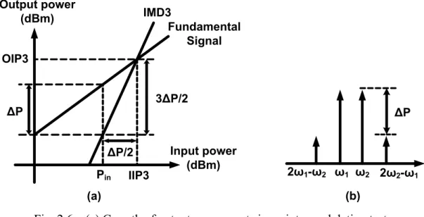
19 3 2ω2 −ω2 =ω2 4 3 ( , , ) 2 2 2 3 3 2 H jω jω jω A − compression or expansion 3 3 1 3ω 2 3ω 4 1 ( , , ) 1 1 1 3 3 1 H jω jω jω A 4 1 ( , , ) 2 2 2 3 3 2 H jω jω jω A Third harmonics This effect causes some distortion at our desired frequency and damages the desired signals. Therefore third intercept point (IP3) is used to characterize this behavior. This parameter is measured by supplying a two-tone signal to the system. This input signal must be chosen to be sufficiently small in order to remove
higher-order nonlinear terms. In a typical test, A1=A2=A, hence the magnitude of
third-order intermodulation products grows at three times the rate at which the fundamental signal on a logarithmic scale when input signal increases. The third-order intercept point is defined to be the point at which third-order intermodulation product equals to the fundamental signal, and the corresponding input signal is called input IP3 (IIP3) and the corresponding output signal is called output IP3 (OIP3). The AIP3, therefore, can be obtained by setting IM3 =1 and expressing as
) , , ( ) ( 3 4 2 2 1 3 1 1 2 3 ω ω ω ω j j j H j H AIP − = (2-26)
Besides, a quick method of measuring IIP3 is as follows. As shown in Fig. 2.6, If the power of the two-tone signal, Pin, is small enough to ignore higher order nonlinear
terms, then IIP3 can be expressed as dBm in dB dBm P P IIP | 2 | | 3 + Δ = (2-27)
20 (a) (b) Output power (dBm) Input power (dBm) OIP3 IIP3 Pin IMD3 Fundamental Signal ω2 ω1 2ω2-ω1 2ω1-ω2 ΔP/2 ΔP ΔP 3ΔP/2
Fig. 2.6 (a) Growth of output components in an intermodulation test (b) Intermodulation distortion
21
Chapter 3
General Consideration in RF Circuit Design
3.1 Low Noise Amplifier Basic
Low noise amplifier is the first gain stage in the receive path so its noise figure directly adds to that of the system. There, therefore, are several common goals in the design of LNA. These include minimizing noise figure of the amplifier, providing enough gain with sufficient linearity and providing a stable 50 Ω input impedance to terminate an unknown length of transmission line which delivers signal from antenna to the amplifier. Among LNA architectures, inductive source degeneration is the most popular method since it can achieve noise and power matching simultaneously, as shown in Fig. 3.1. The following analysis is based on this architecture.
3.1.1
Low Noise Amplifier Architecture Analysis
In Fig. 3.1, the input impedance can be expressed as
gs s g o s T s gs m s gs m gs s g in C L L at L L C g L C g sC L L s Z ) ( 1 1 ) ( + = = ≈ ⎟ ⎟ ⎠ ⎞ ⎜ ⎜ ⎝ ⎛ = ⎟ ⎟ ⎠ ⎞ ⎜ ⎜ ⎝ ⎛ + + + = ω ω ω (3.1) Fig. 3.1 Common source input stage with inductive source degeneration
22
as shown in (3.1), the input impedance is equal to the multiplication of cutoff frequency of the device and source inductance at resonant frequency. Therefore it can be set to 50 Ω for input matching while resonant frequency is designed to be equal to the operating frequency.
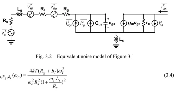
According to prior introduction, the equivalent noise model of common-source
LNA with inductive source degeneration can be expressed as Fig. 3.2, where R is l
the parasitic resistance of the inductor, R is the gate resistance of the device. Note g
that the overlap capacitance Cgd has also been neglected in the interest of simplicity.
Then the noise figure can be obtained by computing the total output noise power and output noise power due to input source. To find the output noise, we first evaluate the trans-conductance of the input stage. With the output current proportional to the
voltage no Cgs and noting that the input circuit takes the form of series-resonant
network, the transconductance at the resonant frequency can be expressed as
s o T s T s gs o m in m m R L R C g Q g G ω ω ω ω ( + ) = 2 = = (3.2)
where Qin is the effective Q of the amplifier input circuit. So the output noise power
density due to the source can be expressed as
2 2 2 2 . , ) 1 ( 4 ) ( s s T s o T eff m Rs o Rs a R L R kT G S S ω ω ω ω + = = (3.3)
23 2 2 2 2 , , ) 1 ( ) ( 4 ) ( s s T s o T l g o R R a R L R R R kT S l g ω ω ω ω + + = (3.4)
Furthermore, channel current noise of the device is the dominant noise contributor, and its noise power density associated with the correlated portion of the gate noise can be expressed as 2 , , ) 1 ( 4 ) ( s s T do o i i a R L g kT S ngc nd ω γκ ω + = (3.5)
where γ is the coefficient of channel thermal noise, α =gm/gd0 and 2 2 2 5 2 1 5 ⎥⎦ ⎤ ⎢ ⎣ ⎡ + + = γ δα γ δα κ c cQL (3.6) gs s o L R C Q ω 1 = (3.7)
The last noise term is the contribution of the uncorrelated portion of the gate noise, and its output noise power density can be expressed as
2 , ) 1 ( 4 ) ( s s T do o i a R L g kT S ngu ω γξ ω + = (3.8) where ) 1 )( 1 ( 5 2 2 2 L Q c + − = γ δα ξ (3.9) Ls Cgs vgs gmvgs ro ind2 Rg 2 ngc i 2 Rg v Rl 2 Rl v Lg Rs 2 s v 2 ngu i 2 out i
24
According to (3.3), (3.4), (3.5) and (3.8), the noise figure at the resonant frequency can be expressed as ⎟⎟ ⎠ ⎞ ⎜⎜ ⎝ ⎛ + + + = T o L s g s l Q R R R R F ω ω α γχ 1 (3.10) where ) 1 ( 5 5 | | 2 1+ c QL 2 + 2 +QL2 = γ δα γ δα χ (3.11)
From (3.11), we observe that χ includes the terms which are constant,
proportional to QL, and proportional to Q . It follows that (3.11) will contain terms L2
which are proportional to QL as well as inversely proportional to QL. A minimum
noise figure, therefore, exits for a particular QL.
3.1.2
Optimizations of Low Noise Amplifier Design Flow
The analysis of the previous section can now be drawn upon in designing the LNA. In order to pick the appropriate device size and bias point to optimize noise performance given specific objectives for gain and power dissipation, a simple second-order model of the MOSFET transconductance can be employed which accounts for high-field effects in short channel devices. Assume that the drain current, Id, has the form
ρ ρ + = − + − = 1 1 ) ( 2 sat sat ox T gs sat T gs sat ox DS WC v LE V V LE V V v WC I (3.12) where sat T gs LE V V − ≡
ρ . And the (3-7) can be replace as
WL Q R C R WLC Q o L s ox s ox o L ω ω 2 3 2 3 ⇒ = = (3.13)
25 ρ ρ ω + = = 1 1 2 3 2 sat sat o s L DD DS DD D v E R Q V I V P (3.14)
The noise figure can be expressed in terms of PD and Vgs. Two parameters linked to
power dissipation need to be accounted for.
) ( 1 gs gs m T f V C g = ≈ ω (3.15) ) , ( 1 1 2 3 2 2 2 D gs D o s o D sat sat DD L f V P P P R P E v V Q = + = + = ρ ρ ρ ρ ω (3.16) where s o sat sat DD o R E v V P ω 2 3 = .
The noise figure of the LNA, therefore, can be expressed as
) , ( ) 1 ( 5 5 | | 2 1 1 2 2 2 D gs L L T o L s g s l c Q Q f V P Q R R R R F = ⎟ ⎟ ⎠ ⎞ ⎜ ⎜ ⎝ ⎛ + + + ⎟⎟ ⎠ ⎞ ⎜⎜ ⎝ ⎛ + + + = γ δα γ δα ω ω α γ (3.17) In general, there are two approaches to optimize noise figure. The first approach
assumes a fixed transconductance, Gm. The second approach assumes fixed power
consumption.
(1) Fixed Gm optimization: To fix the value of the transconductance, Gm, we need
only assign a constant value to ρ. Once ρ is determined, the optimization of
the noise figure can be obtained by (3.17):
) , ( 0 ) , ( . .
.opt Lopt gs Dopt
D Vgs fixed D D gs P V f F Q P P P V f = ⇒ ⇒ ⇒ = ∂ ∂ (3.18)
From (3.18), we can obtain the optimal width to get the minimal noise figure for a
given Gm under the assumption of matched input impedance. In this approach, the
designer can achieve high gain and low noise performance by selecting the desired transconductance, but its disadvantage is that we must sacrifice the power consumption to achieve minimum noise figure.
26
(2) Fixed PD optimization: An alternative method of optimization fixes the power
dissipation and adjusts device size and bias point to minimize the noise figure.
Once PD is determined, the optimization of the noise figure can be obtained by
(3.19): ) , ( 0 ) , ( . .
.opt Lopt gsopt D
gs P fixed gs D gs P V f F Q V V P V f D = ⇒ ⇒ ⇒ = ∂ ∂ (3.19)
Then the optimum device size can be obtained to get the best noise performance for fixed power dissipation. In this approach, the designer can specify the power dissipation and find the optimal noise performance, but its disadvantage is that the transconductance is held up by the optimal noise condition.
3.1.3
Amplifier stability
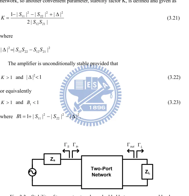
The stability of an amplifier, or its resistance to oscillate, is a very important consideration in a design and can be determined from the S parameters, the matching networks, and the terminations. The non-zero S12 parameter of a two port networks as
shown in Fig. 3.3 provides a feedback path by which the power transferred to the output can be feedback to the input and combined together. Oscillation may occur when the magnitude of reflection coefficient Γ or IN ΓOUT, defined as the ratio of the reflected to the incident wave, exceeds unity. It is expected that a properly designed amplifier will not oscillate no matter what passive source and load impedances are connected to it, which is said to be unconditionally stable and the reflection coefficient is given as 1 | 1 | | | 1 | 1 | | | 11 21 12 22 22 21 12 11 < Γ − Γ + = Γ < Γ − Γ + = Γ s s OUT L L IN S S S S S S S S (3.20)
27
conditionally stable. In such a case, input and load stability circles, the contour of
IN
Γ =1 and ΓOUT=1 for certain frequencies on the Smith chart, are useful to fine the boundary line for load and source impedances that cause stable and unstable condition. The stability circles can be calculated directly from the S parameters of the two port network, so another convenient parameter, stability factor K, is defined and given as
| | 2 | | | | | | 1 21 12 2 2 22 2 11 S S S S K = − − + Δ (3.21) where 2 21 12 22 11 2 | | | |Δ = S S −S S
The amplifier is unconditionally stable provided that
1 > K and |Δ|2<1 (3.22) or equivalently 1 > K and B1 <1 (3.23) where 22 2 2 2 11| | | | | | 1 1= + S − S − Δ B . S Γ Γin Γout ΓL
28
3.2 Down Conversion Mixer Basic
The purpose of the mixer is to convert a signal from one frequency to another. In a receiver, this conversion is from radio frequency to intermediate frequency or zero-IF. Mixing requires a circuit with a nonlinear transfer function, since nonlinearity is fundamentally necessary to generate new frequencies. Fig. 3.4 shows a simplified CMOS Gilbert Cell mixer, which is composed of transcondcutance stage and switching stage.
The RF input must be linear, or adjacent channels could intermodulate and interfere with the desired channel. And the third-order intermodulation term from the two other signals will be directly on top of the desired signal. The LO input need not be linear, since the LO is clean and of known amplitude. In fact, the LO input is usually designed to switch the upper quad so that for half the cycle M3 and M6 are on and taking all current to output loading. For the other half of the LO cycle, M3 and M6 are off and M4 and M5 are on. This stage will be, therefore, like switch to mixing RF signal to IF signal.
29
3.2.1
Conversion Gain
The gain of mixers must be carefully defined to avoid confusion. The voltage conversion gain of a mixer is defined as the ratio of the rms voltage of the IF signal and rms voltage of the RF signal. Note that the frequencies of these two signals are different. The power conversion gain of a mixer is defined as the IF power delivered to the load divided by the available RF power from the source. If the impedances are both matched to 50 Ω, then the voltage conversion gain and power conversion gain of the mixer are equal when they are expressed in decibels.
Now, we assume that M3-M6 work like an ideal switch, and the conversion transconductance of the mixer can be expressed as
m c g G π 2 = (3.24)
where gm is the transcondcutanc of M1 and M2, and 2/π is produced by switching stage.
3.2.2
Switching Stage
For small LO amplitude, the amplitude of the output depends on the amplitude of the LO signal. Thus, gain is larger for larger LO amplitude. For Large LO signals, the upper quad switches and no further increase occur. Thus, at this point, there is no longer any sensitivity to LO amplitude. Besides, if upper quad transistors are alternately switched between completely off and fully on, the noise will be minimized. Since upper transistor contributes on noise when it is fully off, and when fully on, the upper transistor behaves like a cascode transistor which does not contribute significantly to noise.
The large LO signal is required to let upper quad transistors achieve complete switching. But if the LO voltage is made too large, a lot of current has to be moved into and out of the transistors during transitions. This can lead to spikes in the signals
30
and can actually reduce the switching speed and cause an increase in LO feed-through. Thus, too large a signal can be just as bad as too small a signal.
3.2.3
Mixer Noise
Noise figure for a mixer is defined as
Total output noise power at the IF Noise Factor
Output noise power at IF due to input source
= (3.25)
In general, the noise figure of the mixer is divided to two categories, single-sideband (SSB) noise figure and double-sideband (DSB) noise figure. The difference between the two definitions is the value of the denominator in (3.25). In the case of SSB noise figure, only the noise at the output frequency due to the source that originated at the RF frequency is considered, and it is usually used in heterodyne systems. In the case of DSD noise figure, all the noise at the output frequency due to the source is considered (noise of the source at the input and image frequencies), and it is usually used in homodyne systems.
Because of the added complexity and the presence of noise that is frequency translated, mixers tend to be much noisier than LNAs. In generally, mixers have three frequency bands where noise is important:
(1) Noise already present at the IF: The transistors and resistors in the circuit will generate noise at the IF. Some of this noise will make it to the output and corrupt the signal.
(2) Noise at the RF and image frequency: The noise presents at the RF and image frequency will be mixed down to the IF.
(3) Noise at multiples of the LO frequencies: Any noise that is near a multiple of the LO frequency can also be mixed down to the IF, just like the noise at the RF. Beside, the flicker noise will become more important in the homodyne receiver. In the design of the direct down-conversion mixer, how to reduce the flicker noise of upper
31
quad transistors is the important thing. This noise can be reduced by increasing the device size for a given gm.
3.2.4
Port-to-Port Isolation
The isolation between each two ports of a mixer is critical. The LO-RF feed-through results in LO leakage to the LNA and eventually the antenna, whereas the RF-LO feed-through allows strong interferers in the RF path to interact with the local oscillator driving the mixer. The LO-IF feed-through is important because if substantial LO signal exists at the IF output even after low-pass filtering, then the following stage may be desensitized. Fortunately, this feed-through can be reduced largely by used the double-balanced architecture. Finally, the RF-IF isolation determines what fraction of the signal in the RF path directly appears in the IF, a critical issue with respect to the even-order distortion problem in homodyne receivers. The required isolation levels greatly depend on the environment in which the mixer is employed. If the isolation provided by the mixer is inadequate, the preceding or following circuits may be modified to remedy the problem.
3.2.5
Linearity
As far as cascaded stages are concerned, linearity is a very important performance in mixer stage. In general, it will dominate the distortion of the entire receiver. The detail analysis will be introduced in Chapter 4.
32
Chapter 4
-5dBm IIP3 UWB Low Noise Amplifier Using
Complex Derivative Cancellation Technique
4.1
Introduction
Linearity plays an important role in broadband RF systems because nonlinearity degrades system performance with the consequence effects such as harmonic generation, cross-modulation and intermodulation. Of these distortions, the third-order intermodulation (IMD3) is one of the critical terms to be solved. The issue is especially serious to the low noise amplifier (LNA) in broadband system as an LNA needs high gain to suppress noise, while facing a broadband spectrum involving external interferers without much filtering. As such, it has been great attention on linearity improvement to RF circuit designers.
In recent years, several techniques have been proposed to improve the linearity of RF amplifier. Most of them are based on negative feedback circuit. One of the most famous ones is using source degeneration by resistor or inductor. Another scheme is the superposition of auxiliary transistors operated in different bias conditions to cancel the derivative of device transconductance. Such method, referred as derivative superposition or multiple gated transistors (MGTR), offers a good opportunity to extend linearity without increasing power consumption. However the conventional derivative cancellation through DC transconductance analysis is inaccurate at RF frequency. A complex transconductance analysis technique was proposed to search for the optimal design parameters. It is also found adequate to improving IIP3 in a broadband LNA design.
33
In this work, a 3.1~10.6GHz CMOS LNA employing the complex transconductance analysis is reported, with linearity improvement of 5 dB. In the next section the IIP3 analysis of a cascode amplifier is provided, followed by the LNA circuit design, fabrication and measurement results in 0.18 μm CMOS technology.
4.2
UWB LNA Design Consideration
A low noise amplifier (LNA) is an important component at receiver path for wireless communication. It provides a high gain with low noise figure for overall wireless communication system. For various LNA circuit topologies, the common source amplifier is generally popular as it provides a better noise performance with low power consumption. It is especially popular for extreme applications in which ultra low power. A widely used one for narrowband LNA design is a CS amplifier with inductive source degeneration, which has been well analyzed. Because the frequency dependency of the derived Zopt is different from that of Zin, broadband LNA is not feasible using that technique. This is observed in the broadband amplifier realized by employing a multi-order LC matching network. The noise performance is still band-limited. We designed the UWB LNA by employing dual reactive feedback topology, and the theory will be detailed in this paper.
In this chapter discussions are given for broadband noise and input matching realization in a CMOS LNA. Starting from the next section, we first analyze the dual reactive feedback circuit is proposed to achieve broadband noise and input matching, we use transformer simplifying the LNA circuit to save chip area. For better linearity, we try to use multiple gate transistors to improve the linearity of UWB LNA. The following section shows a design example of an UWB LNA implemented in TSMC 0.18µm CMOS process, along with simulation and measurement results.
34
4.3
Dual Reactive Feedback Technique For Broadband
Input Impedance Matching
For this UWB LNA, the proposed solution is a dual reactive feedback topology composing of a capacitive shunt feedback and an inductive series feedback, which individually attain noise and input matching in two different frequency regions to constitute the broadband noise and input matching. These two feedbacks are seamlessly combined by employing an inductor at transistor drain, which conducts different loading conditions for each feedback structure. Then for some reason, three inductors in this circuitry are merged into a transformer to reduce the chip area.
4.3.1
The proposed dual reactive feedback circuit
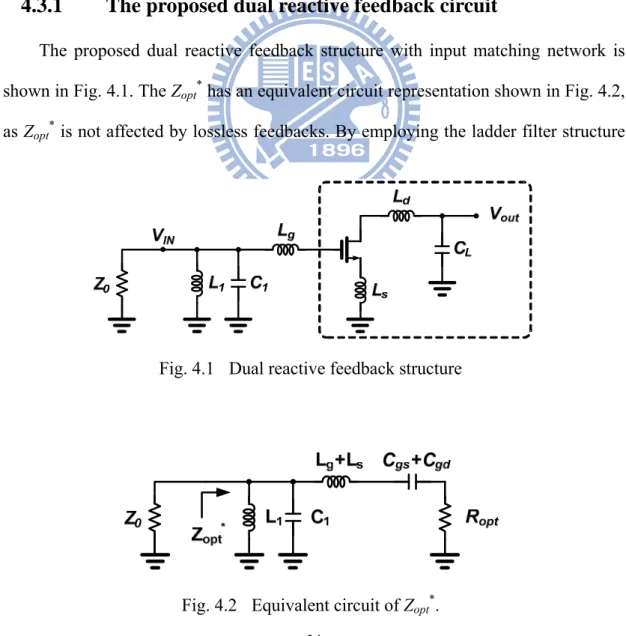
The proposed dual reactive feedback structure with input matching network is shown in Fig. 4.1. The Zopt* has an equivalent circuit representation shown in Fig. 4.2, as Zopt* is not affected by lossless feedbacks. By employing the ladder filter structure
Fig. 4.1 Dual reactive feedback structure