高速與低偏壓砷化銦通道量子井場效電晶體在高頻及邏輯應用之研究
108
0
0
全文
(2) 高速與低偏壓砷化銦通道量子井場效電晶體在高頻及邏輯 應用之研究 Study of High Speed and Low Voltage InAs-Channel Quantum Well Field Effect Transistors for RF and Logic Applications. 研 究 生:吳 建 瑩. Student: Chien-Ying Wu. 指導教授:張. Advisor: Dr. Edward Yi Chang. 翼 博士. 國立交通大學 材料科學與工程研究所 碩士論文. A Thesis Submitted to Department of Materials Science and Engineering College of Engineering National Chiao Tung University In Partial Fulfill of the Requirements For the Degree of Master in Materials Science and Engineering July 2009 Hsinchu, Taiwan, Republic of China. 中華民國九十八年七月.
(3) 高速與低偏壓砷化銦通道量子井場效電晶體在高頻及邏輯應用之 研究. 研究生:吳 建 瑩. 指導教授:張 翼 博士. 國立交通大學材料科學與工程研究所. 摘要. 近年來無線電頻率特別是毫米波、次毫米波頻段的應用,已經對人類的日常生活產 生重大的影響。其所應用的範圍包括有行動通訊、軍事國防、交通指引、雷達系統等; 除此之外,其他一些仍在發展中的應用例如家園防護系統、醫藥分析、高解析度影像感 測系統等,其研究也如火如荼的進行中。而尋找在高頻頻段下仍擁有極高增益、低雜訊 的元件是這類應用的重要關鍵。由於三五族砷化銦鎵材料的高電子遷移率以及量子井場 效電晶體優異的能帶設計,因此三五族砷化銦鎵通道量子井場效電晶體在這方面的應用 展現極大潛力。 在此研究中,成功的製作了四十奈米閘極線寬的砷化銦通道量子井場效電晶體,並 且透過先進的二次閘極蝕刻以及白金閘極掘入技術,使元件展現優異的高頻特性。此研 究比較了在低操作偏壓下(VDS=0.5V)使用此先進製程技術的砷化銦量子井場效電晶體與 未使用此製程的元件,發現透過此兩先進製程步驟,元件展現較佳飽和電流、較低輸出 電導、較小負截止電壓,以及較高的電流增益截止頻率和功率增益截止頻率(可分別達 到440GHz以及190GHz)。除此之外,針對此元件進行雜訊品質的量測,發現即使在高頻 64GHz下,其雜訊指標仍低於2.5分貝。由這些特性可以得知,四十奈米的砷化銦量子井. i.
(4) 場效電晶體是適用於高增益、低雜訊以及低操作偏壓的高頻元件應用。 然而,由於砷化銦材料的窄能隙特性,衝擊離子化效應的現象很容易發生。在這份 研究中,透過實驗數據的分析,具體地證實四十奈米砷化銦量子井場效電晶體的衝擊離 子化效應,其中包括隨著施加偏壓劇烈上升的汲極電流以及在VDS>1.0V時所觀察到的鐘 型閘極漏電曲線,此外,還有包括在VDS=1.0V時急遽上升的雜訊指標以及VDS=1.0V時下 降的電流增益等,都是衝擊離子化效應發生的明顯證據。雖然衝擊離子化現象破壞了元 件的特性,然而只要選擇適當的操作偏壓,仍可得到相當優異的元件特色;例如當VDS 在相當低的0.5V時,其轉移電導即可達到1500 mS/mm,還有在高頻64GHz下,其雜訊指 標仍低於3分貝,此外,在此研究中還發現,當施加的偏壓在衝擊離子化即將發生的電 壓前,可得到663GHz極高的電流增益截止頻率。由以上分析可知,只要選擇適當的操 作偏壓,四十奈米砷化銦量子井場效電晶體是相當適合於毫米波以及次毫米波元件應用 的。 這份論文的最後,另外針對四十奈米砷化銦量子井場效電晶體於未來高速邏輯電晶 體運用做評估,發現在低偏壓下(VDS=0.5V)元件展現相當優異的邏輯特性,包括其汲極 引致能障下降是相當低的50mV/V,而次臨界擺幅也是相當低的89mV/decade,此外,此 元件的閘極延遲時間低於1.0psec,而與Si NMOSFET做比較,其閘極延遲時間也是較低 的。而這些研究結果可以證實四十奈米砷化銦量子井場效電晶體是極有潛力作為未來後 矽半導體世代高速邏輯電晶體的使用。. ii.
(5) Study of High Speed and Low Voltage InAs-Channel Quantum Well Field Effect Transistors for RF and Logic Applications. Student: Chien-Ying Wu. Advisor: Dr. Edward Yi Chang. Department of Materials Science and Engineering National Chiao Tung University. Abstract Recently, wireless communication applications at millimeter wave band and sub-millimeter wave bands have gained a lot of momentum. The applications include wireless systems, cellular backbone, national weaponry, traffic guidance, radar systems, etc. Besides, emerging millimeter wave applications such as homeland security, medical diagnosis, and high-resolution image sensor are also in development rapidly. Therefore, development of the devices possessing both high frequency features and low noise characteristics is becoming urgent. High indium content InGaAs-based QWFETs are particularly promising because the excellent electrical properties of InxGa1-xAs material and the superior band-gap design of QWFET. In this study, the 40 nm InAs QWFETs processed with advanced two-step recess and Pt gate sinking technologies for RF applications are fabricated. The developed 40 nm InAs QWFETs with these advanced processes exhibit better performance than the conventional InAs QWFETs at low applied voltage such as better current saturation, lower output conductance (go), smaller negative threshold-voltage (VT), higher current-gain cut-off frequency (fT) of 440 GHz and higher maximum oscillation frequency (fmax) of 190 GHz. Besides, the 40 nm InAs QWFETs with advanced processes also exhibit the minimum noise figure of lower than 2.5 dB up to 64 GHz when biased at VDS of 0.5 V. The excellent. iii.
(6) electronic performances indicate the developed 40 nm InAs QWFETs are suitable for high-gain, low noise and low voltage applications. However, because of the narrow energy band-gap of InAs channel material, the impact ionization occurred easily. In this study, the investigation of impact ionization phenomena in 40 nm InAs QWFETs is presented. The evidences of the occurrence of impact ionization in InAs QWFETs include the high output conductance with the increase of VDS, a hump in the curve of gate leakage current at VDS higher than 1.0 V, the drastically increase of minimum noise figure at VDS of 1.0 V, and the reduction of fT at VDS of 1.0 V. Although the impact ionization degrades the performance of the devices, the excellent characteristics can still be achieved with optimal bias selection. The devices show transconductance over 1500 mS/mm at VDS of 0.5 V. Besides, low noise figure of less than 3 dB with an associated gain of 7 dB up to 64 GHz at VDS of 0.8 V are observed. And the extremely high fT of 663 GHz can be obtained if the devices are biased near the occurrence of impact ionization. Therefore, with optimal bias conditions, InAs QWFETs can achieve tremendous high performance for high-speed sub-millimeter wave applications. In addition to high frequency RF applications, the evaluations of 40 nm InAs QWFETs for high-speed logic applications have also been demonstrated in this study. The devices show outstanding logic performance in low applied voltage (VDS=0.5 V). The drain induced barrier lowering (DIBL) is 50 mV/V, subthreshold swing (S) is 89 mV/decade, and intrinsic gate delay (CV/ION) is less than 1.0 psec. When comparing to the mature Si technology, the InAs QWFETs exhibit smaller gate delay time. Besides, InAs QWFETs show much higher ION/IOFF performance than the most advanced InSb QWFETs. These results demonstrate that the 40 nm InAs QWFETs have great potential for future high-speed and low-voltage logic applications.. iv.
(7) 誌 謝. 能夠順利完成這份碩士學程,首先必須對指導教授張翼老師表達深深 地感謝之意,感謝老師在實驗上提供我們豐富的儀器資源,以及在學問上 給予我們的熱心指導,感謝老師您的鼓勵支持,使我能夠順利的完成學業。 再來要感謝我的指導學長郭建億博士,在碩士班兩年期間,無論是在 生活上、課業上或實驗上所給予的勉勵與指導,沒有學長的強力支援,我 是無法順利完成碩士學位的。 另外,還要感謝元智大學許恆通博士在實驗上的協助,沒有許博的專 業電路模擬,良好的電性成果將被埋沒。此外也要感謝日本 T.I.Tech. Y. Miyamoto 教授及 T. Yamaguchi 先生在電子束微影系統上的專業協助。感謝 國家奈米元件實驗室(NDL)的工程師及交大奈米中心,同時提供優良的儀器 設備與環境,使實驗能夠更加順利進行。 感謝 CSD Lab 的學長姐、同學、學弟妹以及秘書助理們的鼓勵幫助, 有了你們的陪伴,使我碩士班兩年的生活豐富精彩。 最後,我要特別感謝在我的背後精神上支持的家人,感謝您們的關心、 鼓勵與包容,使我無後顧之憂,能夠專心且順利地完成學業. v.
(8) Contents. Abstract (in Chinese)…………………………………...…………………….…i Abstract (in English)………………………………………..…………………iii Acknowledge (in Chinese)……………………………………………...………v Contents…………………………………………………….………………...vi Table Captions…………………………………….…………………………ix Figure Captions…………………………………………….……………….….x. Chapter 1 Introduction………………………………………………………1 1.1 General Background and Motivation………….………………………….……………..1 1.2 Outline of the Thesis…….……...…………………………………….………………....3. Chapter 2 Overview of III-V Quantum-Well Field-Effect Transistors (QWFETs)……………………………....................................................………5 2.1 The Theory of III-V QWFETs…………....................................………….……………..5 2.2 The Structure of III-V QWFETs……….....……………....................…………......……6 2.3 III-V QWFETs for High Frequency Millimeter/Sub-Millimeter Wave Applications…...7 2.4 Evaluations of III-V QWFETs for Beyond-CMOS Logic Applications……………...…7. Chapter 3 Fabrications of InAs-Channel Quantum-Well Field-Effect Transistors (QWFETs)……………………………………………….……….13 3.1 Mesa isolation…………………………………………………………………………..13 3.2 Ohmic Contact Formation….……………………………………….………………......14 3.3 Electron Beam Lithography Process for Nano T-shaped Gate….……………………...14. vi.
(9) 3.4 Gate Recess Process (Two-Step Recess Process) and Gate Formation……………...... 15 3.5 Device Passivation…………………………………..………………………….………16 3.6 Airbridge Formation………………………………………………………………….…17. Chapter 4 Fundamentals of Electrical Characteristics for InxGa1-xAs QWFETs………………………………………………………….…………....23 4.1 DC Characteristics………………………………………….…………………………..23 4.2 Transmission Line Model (TLM)……………………………………………………...25 4.3 Scattering Parameters…………………...……………………………………...……….26 4.4 Current-Gain Cut-off Frequency (fT) and Maximum Oscillation Frequency (fmax)….…28 4.5 Device Modeling Technique……………………………………………………………29 4.6 Noise Figure…………………………………………………...………………………..30. Chapter 5 Experimental Results and Discussions……………….………….37 5.1 40 nm InAs-Channel Based QWFETs for High-Speed and Low-Voltage RF Applications by using Two-Step Recess and Pt Gate Sinking Processes…….................................…37 5.1.1 Introduction…………………………………………….……..……………...…….37 5.1.2 Experiment……………………………………………………………...………….39 5.1.3 Result and discussion……………………………………………………...……….40 5.1.4 Conclusion…………………………………..……………………………………..43 5.2 Comprehensive Study of Impact Ionization Phenomena in 40 nm InAs-Channel Based QWFETs……….…………...…………………………………………………………...52 5.2.1 Introduction…………………………………………….…………...…..………….52 5.2.2 Experiment…………………………………………………………...…………….53 5.2.3 Result and discussion……………………….…………..………………………….54 5.2.4 Conclusion……………………………………..…………………………………..57. vii.
(10) 5.3 Evaluation of 40 nm InAs-Channel Based QWFETs for High-Performance and Low-Voltage Logic Applications ………………………...........................................…66 5.3.1 Introduction………………………………………...…………….……..………….66 5.3.2 Experiment…………………………………………...…………………………….67 5.3.3 Result and discussion………………………………...…………………………….68 5.3.4 Conclusion………………………………………………..………………………..71. Chapter 6 Conclusion…………………...........…..…………………………...84. Reference…………………………………...............………………………….86. viii.
(11) Table Captions. Chapter 1 Table 1.1 Physical properties of electron and hole of Si, Ge, and main III-V semiconductors………………….……….....……………………………………4. Chapter 2 Table 2.1 Best performance of InP HEMTs and GaAs MHEMTs in high speed and low noise aspect published in recent years.....................................................................12. Chapter 5 Table 5.1 Summary of extracted RF parameters for 40 nm InAs/In0.53Ga0.47As QWFETs at VDS of 0.5 V with/without two-step recess and Pt gate sinking process…………51 Table 5.2 Extracted intrinsic capacitances of a 0.04 μm × 40 μm InAs/In0.53Ga0.47As QWFETs with different drain-source voltage………………………………...………………65. ix.
(12) Figure Captions. Chapter 1 Fig. 1.1 The trend of transistor technology………………………….…………………………4. Chapter 2 Fig. 2.1 Conventional QWFET structure………………………………..…………….……....9 Fig. 2.2 Band Diagram of InxAl1-xAs/InxGa1-xAs QWFET……………………...…………….9 Fig. 2.3 The common expitaxial structures of the InxGa1-xAs based QWFETs for high speed application………………………………………………...…………………………10 Fig. 2.4 Electrical figures of merit of a transistor as a switch……………………….………..11 Fig. 2.5 Evaluation methodology of QWFETs for logic performance………………….…….11. Chapter 3 Fig. 3.1 E-Beam Lithography process flow for nano T-shaped gate………………………….18 Fig. 3.2 The side view of tri-layer photoresist profile for 40 nm T-shaped gate………….…..18 Fig. 3.3 The top view of tri-layer photoresist profile for 40 nm T-shaped gate…. ………......19 Fig. 3.4 The bottom photoresist profile of 40 nm T-shaped gate foot………………………..19 Fig. 3.5 Illustration of two-step recess process flow………………………............……….....20 Fig. 3.6 Cross-sectional view of gate formation after two-step recess……………………….21 Fig. 3.7 SEM images of 40 nm T-shaped gate……………………………………………….21 Fig. 3.8 SEM images of the airbridge……...……………………………………………….22. Chapter 4 Fig. 4.1 Band diagrams of QWFET at three different locations along the channel………….31. x.
(13) Fig. 4.2 Drain current of III-V QWFETs predicted by Eq. (4-4)….............................……….31 Fig. 4.3 TLM pattern……………….………………………………………………...……….32 Fig. 4.4 The illustration of utilizing TLM to measure ohmic contact resistance….............….32 Fig. 4.5 The equivalent two-port network schematic at low frequency………………………33 Fig. 4.6 The equivalent two-port network schematic at high frequency…………………...…33 Fig. 4.7 The device layout used in this study………………………………………………....34 Fig. 4.8 The block diagram with determined parasitic elements for the overall device structure…...................................................................................................................35 Fig. 4.9 Functional blocks of the equivalent circuit model, divided according to the scalability with device size…………………….……………………..........................................35 Fig. 4.10 Analyzed electric field plot of the 2x50um device at 10 GHz. (a) with the source buses of the device (b) without the source buses of the device……..........………..36. Chapter 5 Fig. 5.1.1 Epitaxial structure of InAs/In0.53Ga0.47As QWFETs in this study……………....…44 Fig. 5.1.2 SEM images of the 40 nm T-shaped gate photoresist and the finished 40 nm gate after the two-step recess process..............................................................................44 Fig. 5.1.3 Drain-source current versus drain-source voltage curves of 40nm InAs QWFET without two-step recess and gate sinking process..................................................45 Fig. 5.1.4 Drain-source current versus drain-source voltage curves of 40nm InAs QWFET with two-step recess and gate sinking process……….…………………………..45 Fig. 5.1.5 Transconductance versus gate-source voltage of 40nm InAs QWFET without two-step recess and gate sinking process of In0.7Ga0.3As QWFETs……………...46 Fig. 5.1.6 Transconductance versus gate-source voltage of 40nm InAs QWFET with two-step recess and gate sinking process of In0.7Ga0.3As QWFETs….................................46. xi.
(14) Fig. 5.1.7 Frequency dependence of the current gain (H21) and the power gain (MAG/MSG) of 40nm InAs/In0.53Ga0.47As composite channel QWFETs without two-step recess and gate sinking process. The frequency range was from 4 to 40 GHz, and the device was biased at VDS = 0.5V and VGS = -0.65V……………..………………47 Fig. 5.1.8 Frequency dependence of the current gain (H21) and the power gain (MAG/MSG) of 40nm InAs/In0.53Ga0.47As composite channel QWFETs with two-step recess and gate sinking process. The frequency range was measured to 40 GHz, and the device was biased at VDS = 0.5V and VGS = -0.2V. ……………………………48 Fig. 5.1.9 Measured minimum noise figure (NFmin) and the associated gain of the 40nm InAs QWFETs with two-step recess and gate sinking process at VDS = 0.5V and the applying DC power was 4.33mW.……….…………………………………….....49 Fig. 5.1.10 Cutoff frequency of 40nm InAs QWFETs and 80 nm Si nMOSFETs as a function of the power dissipation…………………………………….................................50 Fig. 5.2.1 Epitaxial structure of InAs/In0.53Ga0.47As composite channel QWFETs in this study……………………………………………………………………………59 Fig. 5.2.2 Drain-source current versus drain-source voltage curves of InAs/In0.53Ga0.47As composite channel QWFETs with different gate voltage.......................................60 Fig. 5.2.3 Output conductance of InAs/In0.53Ga0.47As composite channel QWFETs as a function of drain voltage with different gate voltage…………………………….61 Fig. 5.2.4 Gate leakage current of InAs/In0.53Ga0.47As composite channel QWFETs as a function of gate voltage at different drain bias……………….…..……………...62 Fig. 5.2.5 Measured minimum noise figure (NFmin) and associated gain of InAs/In0.53Ga0.47As composite channel QWFETs as a function of frequency at VDS = 0.5-1.0 V…...…63 Fig. 5.2.6 (a) The current gain (H21) and maximum available (stable) gain (MAG/MSG) as a function of frequency at VDS = 0.9 V. (b) The fT and fmax versus drain voltage at gate bias of 0 V.…………………………………………………………………..64. xii.
(15) Fig. 5.3.1 Epitaxial structure of InAs/In0.7Ga0.3As composite channel QWFETs in this study………………………………….…………...…………………………….72 Fig. 5.3.2 Drain-source current versus drain-source voltage curves for 40nm InAs/In0.7Ga0.3As QWFET with two-step recess and gate sinking process...........................................72 Fig. 5.3.3 Transconductance versus gate-source voltage of 40 nm InAs/In0.7Ga0.3As QWFET with two-step recess and Pt gate sinking process.………..………………………..73 Fig. 5.3.4 Two terminal gate-drain breakdown characteristics of 40nm InAs/In0.7Ga0.3As QWFET with two-step recess and gate sinking process…………………………74 Fig. 5.3.5 Current gain cut-off frequency (fT) vs. IDS at different VDS of fabricated 40nm InAs/In0.7Ga0.3As composite channel QWFET…………………………………..75 Fig. 5.3.6 Frequency dependence of the current gain (H21) and the power gain (MAG/MSG) of the 40nm InAs/In0.7Ga0.3As composite channel QWFETs. The frequency range was from 5 to 80 GHz, and the device was biased at VDS = 1.0 V………………76 Fig. 5.3.7 Cutoff frequency of 40 nm InAs QWFETs and Si MOSFETs as a function of the power dissipation……………………………………………………...…………77 Fig. 5.3.8 The sub-threshold characteristics (DIBL, S, I ON /I OFF ratio) of 40nm InAs/In0.7Ga0.3As composite channel QWFETs at the VDS of 0.05 and 0.5V……78 Fig. 5.3.9 The methodology for the evaluation of the logic performance of novel devices with non-optimized VT. Different definitions of VT result in a new set of logic parameters of C’V’/I’……………………………………………………………79 Fig. 5.3.10 Gate delay as a function of the selected threshold voltage at VDS = 0.5V………..80 Fig. 5.3.11 Gate delay of InAs, InSb QWFETs and Si NMOSFETs as a function of gate length…………………………………………………………………………..…81 Fig. 5.3.12 ION/IOFF ratio as a function of various VT at drain voltage of 0.5 V………….…..82 Fig. 5.3.13 Comparison between gate delay and ION/IOFF of 40 nm InAs QWFETs, 200 nm InSb QWFETs and 40 nm Si MOSFETs……………………………………….83. xiii.
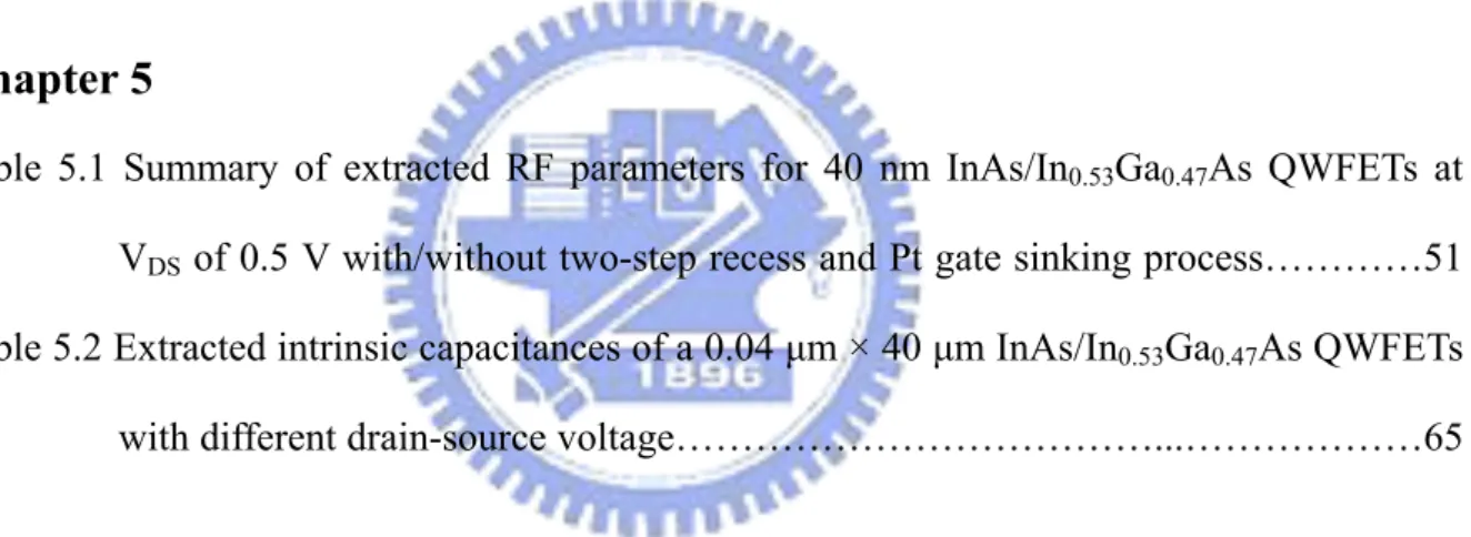
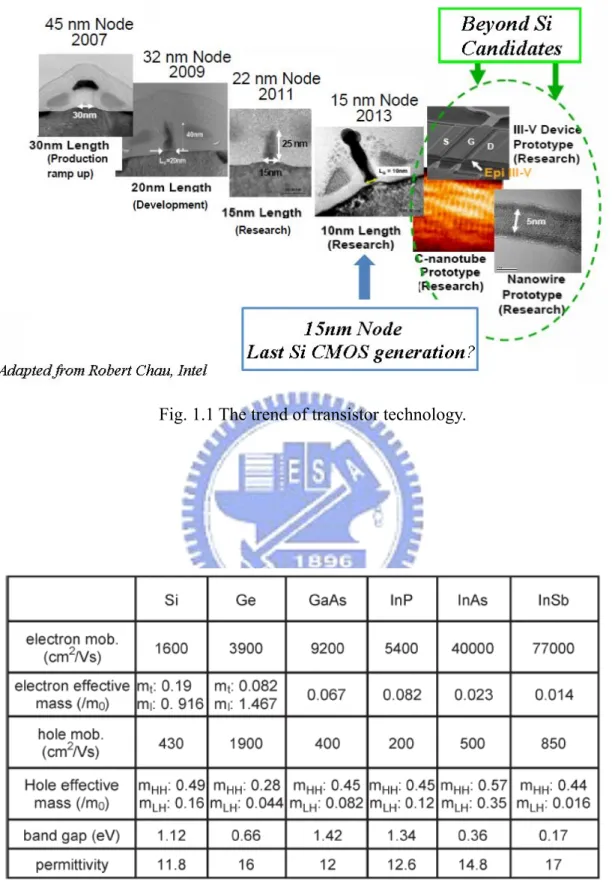
(16) Chapter 1. Introduction. 1.1 General Background and Motivation. Continually scaling down Si-transistors is always the way to sustain Moore’s law for last 30 years. But, it is expected that the dimension will reach about 10 nm by 2011 [1-1], which would be the ultimate limitation for Si CMOS. Fig. 1.1 [1-2, 1-3] lists the trend of transistor technology. Therefore, identifying a new logic device technology becomes an urgent issue. Candidates, which are often mentioned, are carbon nanotube (CNT) transistors, semiconductor nanowires and spintronics [1-4], etc. While the majority of the technologies mentioned above are still in the prototyping stage. On the contrary, III-V devices especially the Quantum Well Field Effect Transistors (QWFETs) gradually unfold potential because of their relatively mature technology and excellent performance. In general, III-V materials own high carrier transport properties like high electron mobility, high electron peak velocity, low electron effective mass, reasonable energy band-gap and high quantum confinement in the channel region. For InAs material used in this research, the bulk electron mobility is around 40000 cm2V-1S-1 at room temperature. The detailed material properties of Si, Ge and III-V materials are listed in Table 1.1 [1-5]. Recently, many researches of III-V devices especially QWFETs with high indium concentration InxGa1-xAs channel materials exhibiting excellent DC and RF performance have been published [1-6, 1-7]. Endowed with these extraordinary electron transport properties, it seems imperative to evaluate the potential of InxGa1-xAs QWFETs for future beyond CMOS logic applications. On the other hand, for future millimeter/sub-millimeter wave wireless-communication. 1.
(17) applications including mobile radio systems and passive imaging systems etc., low noise amplifiers (LNAs) with extremely low noise figure, high gain and low DC power consumption are in highly demand. In order to meet the continuously growing requirement, the technique to improve devices performance becomes more and more rigid and challenging. However, InxGa1-xAs QWFETs also show great potential in this field. InxGa1-xAs QWFETs have demonstrated the best noise/gain performance and low power dissipation under ultra high frequency operation [1-8, 1-9]. Therefore, using InxGa1-xAs QWFETs for future high-speed millimeter wave wireless-communication applications are the most promising. Furthermore, with the further improvement of InxGa1-xAs QWFETs in frequency dependent performance, the applications expanding the radio spectrum resources to sub-millimeter wave (300 GHz - 3 THz) frequency region for new generation of military, telecommunications and radio astronomy applications are also worth expecting. In this study, in order to exhibit the excellent performance of InAs QWFETs in high-speed, low-noise, low-power RF and logic applications, several approaches have been adopted. These efforts include the applications of exquisite electron beam lithography technique for 40 nm gate length, advanced two-step recess fabrication, platinum (Pt) gate sinking process, and other precise process adjustments. As a result of the good electronic transport properties of InAs materials, terrific band-gap engineering design of QWFET and advanced fabrication process, the InAs QWFETs in this study exhibit excellent DC, RF, noise and logic performance, which makes them feasible for future high-speed, low-voltage digital as well as high frequency millimeter/sub-millimeter wave applications.. 2.
(18) 1.2 Outline of this Thesis. This thesis focuses on the study of RF and logic evaluation of 40 nm InAs channel QWFETs. In chapters 2, the overview including the basic mechanism and literature survey of III-V QWFETs is described. The detailed fabricating processes of the InAs QWFETs are introduced in chapter 3. In chapter 4, the fundamentals of electrical DC and RF characteristics of the device are described. The experimental results and discussions are shown in chapter 5 and which are divided into three parts. The first part discusses the effect of advanced two-step recess process and Pt gate sinking process on 40 nm InAs QWFETs for RF application. Due to the narrow energy gap feature of InAs material, the impact ionization phenomena is easily occurred. So in the second part, the impact ionization phenomena of InAs QWFETs are studied and the optimum bias conditions for RF operation are also discussed. Beside the application of InAs QWFETs in high frequency millimeter-wave region, the logic characteristics of InAs QWFETs are also evaluated. In the third part of discussion, the important figures of merit relevant to logic such as gate delay, ION/IOFF, DIBL, and S of the InAs-channel QWFETs are studied. Finally, the conclusion of the thesis is given in chapter 6. The 40 nm InAs QWFETs exhibit great potential both in low-voltage, high-speed, low-noise RF applications as well as high-performance logic applications.. 3.
(19) Fig. 1.1 The trend of transistor technology.. Table 1.1 Physical properties of electron and hole of Si, Ge, and main III-V semiconductors.. 4.
(20) Chapter 2. Overview of III-V Quantum-Well Field-Effect Transistors (QWFETs). 2.1 The Theory of III-V QWFETs. Quantum-well field-effect transistor (QWFET) or called High electron mobility transistor (HEMT) is one of the most mature III-V semiconductor transistors. The first demonstration of this device was made by Fujitsu Lab. in 1980 [2-1]. Fig. 2.1 represents a cross-sectional view of a conventional QWFET structure. The epitaxial layers of the QWFET structure are designed to form two-dimension electron gas (2-DEG) in the channel layer. The explanation of 2-DEG formation by energy band diagram of InxAl1-xAs/InxGa1-xAs Metamorphic HEMT is shown in Fig. 2.2 [2-2]. When the small electron affinity (χ) and high energy band-gap (Eg) InxAl1-xAs material connects to the large electron affinity (χ) and low energy band-gap (Eg) InxGa1-xAs material, due to the Fermi-level (Ef) of these two materials must reach the horizontal balance andχ as well as Eg must remind the same value for each materials, there will generate the discontinuity of conduction band (Ec) in the junction. This discontinuity will cause partial Ec of InxGa1-xAs below the Ef so the mass electrons will accumulate in this 2-DEG quantum well. These electrons move fast in 2-DEG because they were accumulated in intrinsic and high electron mobility InxGa1-xAs material channel. As a result of the terrific band-gap engineering design of QWFETs, the QWFETs can exhibit superior carrier transport characteristics. For the past few years, GaAs-based MHEMTs or InP-based HEMTs with remarkable device performance in high speed applications have been published frequently.. 5.
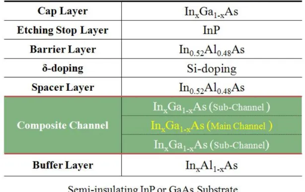
(21) 2.2 The Structure of III-V QWFETs. In general, the epitaxial layers of the InxGa1-xAs-channel QWFETs were grown by molecular beam epitaxy (MBE) or metal organic chemical vapor deposition (MOCVD) on InP/GaAs substrates, and the common expitaxial structures of the InxGa1-xAs-channel QWFETs for high frequency application are shown in Fig. 3.1. As Fig. 2.3 shown, the structure layers from bottom to top are composed of a InxAl1-xAs metamorphic buffer layer, a InGaAs-based channel layer optionally combining with sub-channel, a In0.52Al0.48As spacer layer, a δ-doped carrier supply layer, a In0.52Al0.48As barrier layer, a InP etching stop layer and a highly Si-doped InxGa1-xAs cap layer. The InxAl1-xAs metamorphic buffer layer is used to release the lattice mismatch between InxGa1-xAs channel and GaAs/InP substrate. Therefore, the high indium content (50%-100%) of the InxGa1-xAs channel layer can be achieved in spite of the large lattice mismatch between the active channel layer and the substrate. The adhesion of InxGa1-xAs sub-channels could enhance the electron confinement in the thin and low energy band-gap main channel layer and further improve the electron transport properties [2-3]. The In0.52Al0.48As spacer layer is applied to form heterostructure interface with InGaAs-based channel so that the band diagram discontinuity occurred, and the 2-DEG formed. A δ-doped layer with Si doping concentration could provide extra carriers to the channel layer. And an InP layer can provide a good gate recess etching stop layer as well as a good surface passivation of InxAl1-xAs layer to avoid kink effect and reduce the hot-electron surface damage [2-4]. Besides, with the use of the InP etching stop layer, the lateral recess length (Lr) can be easily controlled and RF performance can be improved [2-5, 2-6]. Finally, the highly Si-doped InxGa1-xAs cap layer is used to reduce the contact resistance.. 6.
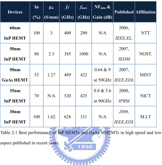
(22) 2.3 III-V QWFETs for High Frequency Millimeter/Sub-Millimeter Wave Applications. In recent years, the millimeter-wave has shown large impact on our daily communication life. The applications of millimeter wave for communication include gigabit wireless system, cellular backbone, national weaponry, traffic guidance, radar, radio navigation device, etc. Besides, other emerging applications such as homeland security, medical diagnosis, and high-resolution image sensor have even moved to sub-millimeter wave band. With the rapid progress of communication industries, the required performances for the high frequency components are getting more and more rigid. Among all the electronic devices, III-V based compound semiconductor devices such as pseudomorphic GaAs HEMTs (PHEMTs), metamorphic GaAs HEMTs (MHEMTs), lattice-matched or pseudomorphic high indium mole fraction InxGa1-xAs channel InP HEMTs have shown great potential in millimeter/sub-millimeter wave applications. Recently, by advanced improvement of process, the InxGa11-xAs QWFETs in literature have achieved current-gain cutoff frequency (fT) of 628 GHz [2-7], maximum oscillation frequency (fmax) above 1 THz [2-8], extrinsic transconductance (gm) of 3 S/mm [2-9], and minimum noise figure (NFmin) of 0.8 dB at 90 GHz [2-10]. Consequently, they are regarded as key devices for next-generation millimeter/sub-millimeter wave systems. Table 2.1 [2-7~2-11] lists the best record of QWFETs in high speed and low noise catalog in the last three years.. 2.4 Evaluations of III-V QWFETs for Beyond-CMOS Logic Applications. For the post-Si era of logic CMOS, III-V compound semiconductors have emerged as promising channel materials, which is not only for their potential in high-speed and low-power performance, but the III-V device technology is relatively mature and reasonably. 7.
(23) reliable [2-12] compared to other novel devices such as carbon-nanotube transistors and semiconductor nanowires. Recently, nano gate length InxGa1-xAs QWFETs with outstanding logic performance at low supply voltage have been demonstrated [2-13]. Therefore, using III-V materials as channel for future logic CMOS applications have been noticeable. In digital application, a transistor operates as a switch, which is different from analog for microwave or millimeter wave application. As seen from the Fig. 2.4, there’re some electrical figures of merit of a transistor as a switch in digital application [2-13], like drain-induced barrier lowering (DIBL), subthreshold slope (S), on-state and off-state current ratio (ION/IOFF), and the gate delay time (CV/I). But for non-optimized devices, arbitrary selections of threshold voltage (VT), ION and IOFF can easily result in an over-estimation of the logic parameters. In this study, the methodology proposed by Chau [2-12, 2-14] to analyze new devices which often feature non-optimized values of VT were adopted. The evaluation methodology is shown in Fig. 2.5. First, select gate-source voltage at drain-source current of 1 mA/mm as the VT. Then select ION as 2/3 VCC swing above VT, and IOFF as 1/3 VCC swing below VT. Based on this definition, the logic parameters, such as subthreshold slope, DIBL and ION/IOFF ratio of InxGa1-xAs QWFETs can be extracted. The steepness of the device transition between the ON and OFF states is evaluated through the subthreshold slope and ION/IOFF ratio. And the tightness of the threshold voltage is evaluated by drain-induced barrier lowering (DIBL), for which measures the change in VT as a result of a change in VDS. If DIBL is small, VT is insensitive to circuit design details and manufacturing variations. Subthreshold slope and DIBL often go hand in hand and they reflect the overall electrostatic integrity of the device. Besides, device capacitance impacts the switching speed. An important figure of merit in this regard is the transistor delay (CV/I), which is a measure of the time that it takes for a transistor to switch an identical one.. 8.
(24) Fig. 2.1 Conventional QWFET structure. Fig. 2.2 Band Diagram of InxAl1-xAs/InxGa1-xAs QWFET. 9.
(25) Fig. 2.3 The common expitaxial structures of the InxGa1-xAs based QWFETs for high speed application.. 10.
(26) Fig. 2.4 Electrical figures of merit of a transistor as a switch. Fig. 2.5 Evaluation methodology of QWFETs for logic performance. 11.
(27) In Devices. gm. fT. fmax. NFmin &. Published Affiliation. (%) (S/mm) (GHz) (GHz) Gain (dB) 2006,. 60nm 100. 3. 400. 290. N/A. NTT. InP HEMT. IEEE,EL.. 50nm. 2007, 80. 2.3. 385. 1000. N/A. NGST. IEDM. InP HEMT 0.64 & 9. 50nm 53. 1.27. 489. 2007,. 422. MINT at 59GHz IEEE,EDL. GaAs HEMT. 0.8 & 5.6. 35nm 70. N/A. 520. 2008,. 425. NICT at 90GHz. InP HEMT. IPRM 2008,. 30nm 100. 1.62. 628. 331. N/A. M.I.T IEEE,EDL. InP HEMT. Table 2.1 Best performance of InP HEMTs and GaAs MHEMTs in high speed and low noise aspect published in recent years.. 12.
(28) Chapter 3 Fabrications of InAs-Channel Quantum-Well Field-Effect Transistors (QWFETs). The fabricated QWFETs in this study bring together novel designs to enhance the electronic properties. For instance, the QWFETs with small gate length (Lg) of 40nm can increase the electronic field under the gate so the electron will accelerate; the tunneling cap layer with highly doping can efficiently minimize parasitic resistances [3-1]; the application of two-step recess process can scale-down gate electrode to channel thickness so that the short channel effect is released [3-2]; and the application of Pt gate sinking process can enhance the schottky gate work function. Besides, by the precise time control of Pt gate sinking annealing, the gate electrode can be further close to channel layer so as to speed up electron transport [3-3].. The process flows of QWFETs fabrication in this study are listed below. 1.. Active region formation (Mesa isolation). 2.. Ohmic contact formation. 3.. Electron Beam Lithography process for nano T-shaped gate. 4.. Gate recess process (Two-step recess process) and gate formation. 5.. Device passivation. 6.. Airbridge formation. 3.1 Mesa Isolation. For III-V devices, the mesa isolation process is used for the definition of active region. First, the active areas were masked by Shipley S1818 photoresist. Then the phosphoric based. 13.
(29) solution was used to etch InGaAs/InAlAs layers and hydrochloric acid based solution was used to etch InP layer. According to the device structure, the mesa was etched to the buffer layer to provide good device isolation. The etching depth was approximately 2500Å measured by α-step. After the strip of photoresist, the etching profile was carefully checked by scanning electron microscopy (SEM).. 3.2 Ohmic Contact Formation. The photoresist AZ5214E and I-line aligner were used to define the ohmic metal pattern. Unlike the Si-based devices, the lift-off process is used for III-V based device because of the lack of appropriate etching selection between ohmic metals and III-V materials. The undercut profile of the photoresist AZ5214E will benefit the metal lift-off process. The HCl-based solution was used to remove the native oxide on the InGaAs surface before Ohmic metallization. Ohmic metal multilayer Au/Ge/Ni/Au, from the bottom to the top, was deposited by e-gun evaporation system and the thickness was 2400Å. After metal lift-off process, the devices were annealed by rapid thermal annealing (RTA) at 270 oC for 30 sec in forming gas atmosphere. During annealing, germanium atoms will diffuse into the InGaAs cap layer forming heavily doped status so the contact resistance decreased. The specific contact resistance between metal and cap layer can be extracted by the transmission line method (TLM) [3-4]. In general, the typical measured contact resistance must be less than 1 x -6. 2. 10 Ω-cm .. 3.3 Electron Beam Lithography Process for Nano T-shaped Gate. Decreasing gate length (Lg) can increase the electronic field under the gate so as to accelerate the transport property of channel electron. Therefore, it is benefit for devices in. 14.
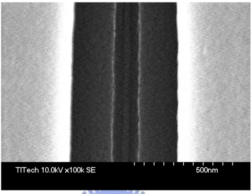
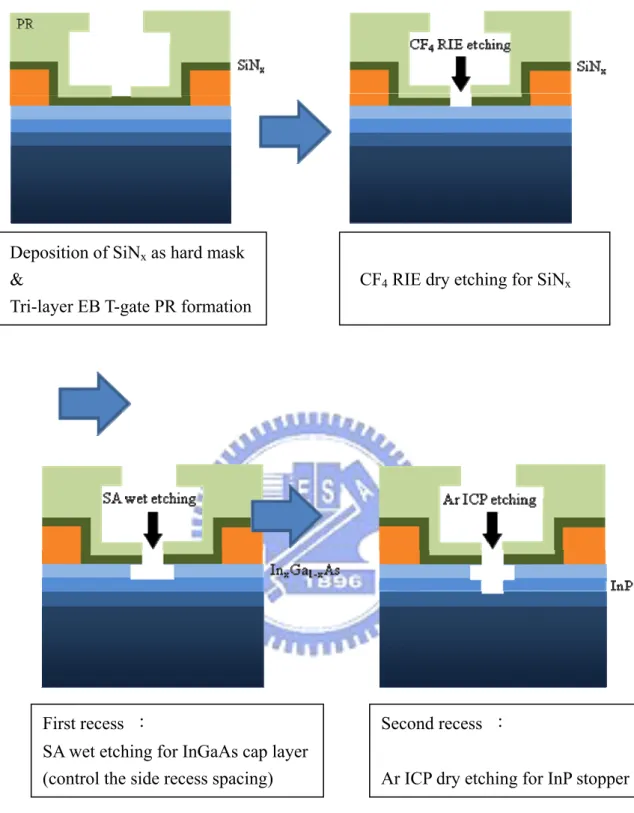
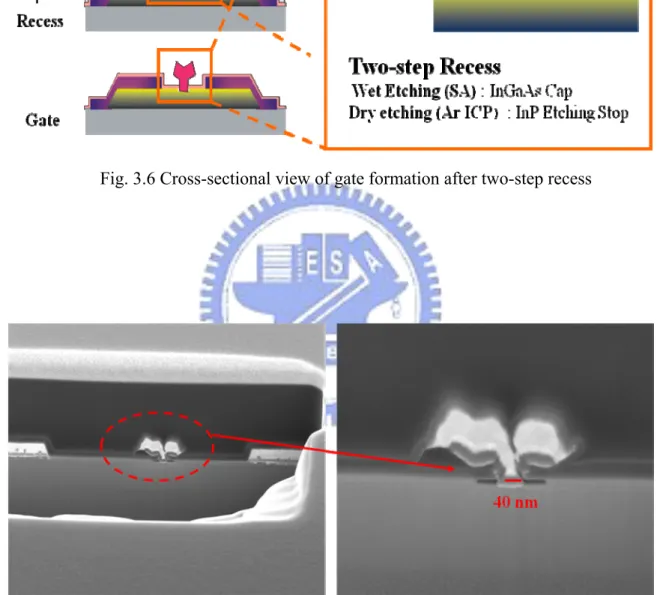
(30) high frequency and high speed applications. T-shaped gate structure was the most common approach for achieving low gate resistance and a small gate foot [3-4]. In this study, the Electron Beam lithography with tri-layer photoresists (ZEP-520/PMGI/ZEP-520) was applied for the T-shaped gate formation. Fig. 3.1 illustrates the process flow of the fabrication of nanometer T-shaped gate. The first E-beam exposure for top two layers was used to define the head (Tee-top) of the T-shaped gate. After that, the ZEP-520 and PMGI development were executed by using xylene and MF622, respectively. Then, high dosed single center exposure with xylene development was used to define the footprint of the bottom ZEP-520 layer. The SEM image of the 40 nm T-shaped gate resist profile is shown in Fig. 3.2-3.4.. 3.4 Gate Recess Process (Two-step Recess Process) and Gate Formation. Through anisotropic CF4 RIE dry etching, the gate foot was precisely replicated on 600Å SiN layer which was deposited by plasma-enhanced chemical vapor deposition (PECVD) before the E-Beam photoresistor formation. Besides, these additional 600Å SiN layer can mechanically support the small Lg of T-shaped gate [3-5]. For gate recess etching, in order to suppress the short channel effect and enhance the electron mobility under the gate, a two-step recess process proposed by T.Suemitsu et al. [3-2] was used. By applying two-step recess process, gate electrode was much close to the channel. Fig. 3.5 illustrates the process flow of two-step recess. The first step of recess was cap layer etching performed by using PH-adjusted solution of succinic (S.A.) and H2O2. The target current after the cap layer recess is a critical parameter to affect the QWFET performance. In order to get the desired recess target, the recess process was controlled by monitoring the non-gated drain-to-source current (IDS). The second step of recess etching was removing the InP etching stop layer under the gate opening by inductive coupled plasma (ICP) with argon ambient. The second step of recess etching resulting gate structure has the gate metal deposited on InAlAs barrier layer. 15.
(31) whereas the InP etching stop layer covers the recess region as illustrated in Fig. 3.6. After recess etching, Pt/Ti/Pt/Au (120/800/600/1800Å) gate metal was evaporated by e-gun evaporation system and lifted off by using ZDMAC remover (ZEON Corporation). For multilayer gate metal (Pt/Ti/Pt/Au), where titanium is a good adhesion layer; platinum acts as a barrier layer to prevent gold from diffusing into GaAs; and gold provides high electrical conductivity. Unlike the traditional GaAs-based QWFETs, in this study for proceeding Pt gate sinking process, the additional 120Å-thickness platinum was applied to the first gate electrode. There’re several advantages of Pt gate sinking process for QWFETs. By precisely annealing time control, Pt can react with As and move toward channel. This function makes the gate electrode further close to channel layer, and it is benefit for device characteristics in high frequency as well as in logic aspects [3-3]. Additionally, Pt gate sinking process provides higher schottky gate work function of 0.8eV for PtAs4 on InAlAs than the traditional work function of 0.4eV and 0.6eV for Ti on InAlAs and InP respectively. Besides, slight reduction in the gate leakage current was also observed owing to the increase in the thickness of the amorphous layer under gate which diminished the leakage path because of the reduction of the grain boundaries [3-6, 3-7]. The final formation of 40nm T-shaped gate was pictured by SEM as shown in Fig. 3.7.. 3.5 Device Passivation. To prevent the device from the mechanical damages and environmental contaminations such as chemicals, gases, and particles; surface passivation of device is necessary. The dielectric layer SiNx is a common choice for III-V device passivation. Before the passivation, the wafer was dipped in the solution of NH4OH:H2O=1:50 for 30 seconds to clean the surface and decrease the surface dangling bonds. And then PECVD system with process pressure of 900 mtorr, process temperature of 200°C, process time of 10 minutes, and process gases of. 16.
(32) silane, ammonia, and nitrogen was used for depositing the silicon nitride film. The silicon nitride film thickness was about 600 Å and the reflection index was 2.0 as inspected by N&K anaylzer. After the passivation process, the contact via was opened by CF4 RIE etching for interconnections.. 3.6 Airbridge Formation. Airbridge process is used to interconnect the sources of FETs, to cross over a lower level of metallization, or to connect the top plate of a MIM capacitor for adjacent metallization. And because of the lowest dielectric constant, low parasitic capacitance of air, and the high electronic conductance of gold; airbridge process is used extensively in III-V analog devices and MMICs for interconnections. For airbridge procedure, firstly the photoresistor was coated on the metal pad, and followed by a whole wafer deposited with thin Ti/Au/Ti. Then, a second photoresistor was patterned, and the gold of 2μm was electroplated. After that, the top photoresist layer, thin Ti/Au/Ti metal, and bottom resist layer were removed individually, leaving only the plated air-bridge. The SEM image of the airbridge is shown in Fig. 3.8.. 17.
(33) Fig. 3.1 E-Beam Lithography process flow for nano T-shaped gate. Fig. 3.2 The side view of tri-layer photoresist profile for 40 nm T-shaped gate. 18.
(34) Fig. 3.3 The top view of tri-layer photoresist profile for 40 nm T-shaped gate. Fig. 3.4 The bottom photoresist profile of 40 nm T-shaped gate foot. 19.
(35) Deposition of SiNx as hard mask & Tri-layer EB T-gate PR formation. CF4 RIE dry etching for SiNx. First recess :. Second recess :. SA wet etching for InGaAs cap layer (control the side recess spacing). Ar ICP dry etching for InP stopper. Fig. 3.5 Illustration of two-step recess process flow. 20.
(36) Fig. 3.6 Cross-sectional view of gate formation after two-step recess. Fig. 3.7 SEM images of 40 nm T-shaped gate. 21.
(37) Fig. 3.8 SEM image of the airbridge. 22.
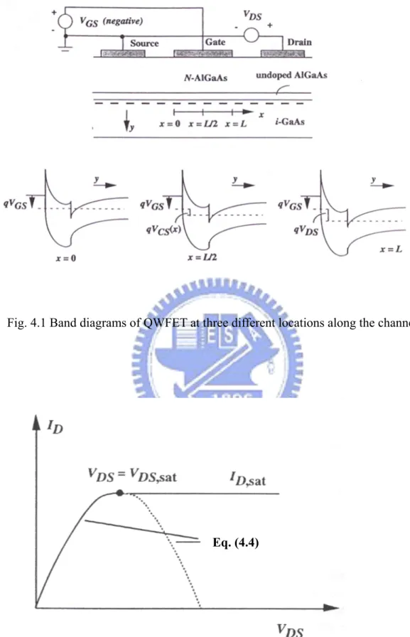
(38) Chapter 4. Fundamentals of Electrical Characteristics for InxGa1-xAs QWFETs. After the device fabrication, DC and RF performance of the QWFETs were measured by using on-wafer measurement. For the DC measurement, the I-V characteristics were obtained by using an HP4142B Modular DC Source/Monitor and SUSS PA200 Semi-Auto Probe Station. The Transmission Line Model (TLM) method for determining specific contact resistance was adopted by using 4-wires measurement. The S-parameters were measured by HP8510XF Vector Network Analyzer using on-wafer GSG probes from Cascade MicroTech. However, finding the RF behavior of a device on a wafer was a complicated process. For conventional RF measurement of a packaged device, the wafer needs to be diced and then an individual die should be mounted into a text fixture. Discriminating between the die’s and the fixture’s responses became an issue. Furthermore, fixturing die was a time-consuming process, and making it impractical for high-volume screening. Thus the need for on-wafer RF characterization was arisen [4-1]. In this study, de-embedding which must also be performed to discover the true RF performance of the device is discussed.. 4.1 DC Characteristics [4-2]. The band diagrams at three different locations along the channel are illustrated in Fig. 4.1. There is a potential drop of channel charge density in the direction parallel to the channel, causing q’CH to be a function of the position x. In order to relate the QWFET equations to the well-developed MOSFET equations, a per area gate oxide capacitance was define as C’OX. Therefore, the channel charge sheet density is expressed as:. 23.
(39) q'CH C 'OX [VGS VT VCS ( )]. (4-1). Here the channel-to-source potential is resulting from the applied Gate-Source voltage (VGS) and Drain-Source voltage (VDS). VT is threshold voltage and the x means the position along the channel. The additional potential VCS(x) is called the channel-source potential. When VDS ≠ 0, the channel-source potential varies with x and the potential difference is the potential between any point x along the channel with respect to the source. The channel current equation I= qAμnε (A=area) is proportional to the cross-section area of the current conduction, the charge density, the mobility μn, and the electric field. Therefore, the form of the channel current equation in QWFET is obtained: I CH ( ) WCOX n [VGS VT VCS ( )]. dVCS ( ) d. (4-2). We note that q’CH is a negative quantity in QWFET, since electrons accumulated in the channel are negative charges. Besides, if we choose x = L at the drain, this constant channel current is equal to the negative of the drain current. Hence, we have ID =- ICH, and we find:. . L. 0. I DS dx C 'O. VCS L . C. OX. n [V ( GS ) V (T ) V ( CS ) ( )]dV CS ( ). (4-3). VCS O . To carry out the integration in Eq. (4-3), we deal with the linear operating region first so that current saturation due to channel pinch off at the drain does not occur. In the linear region, the boundary conditions are VCS(L) = VDS and VCS(0) = 0. Hence, Eq. (4-3) leads to: ID . W g C ' OX n V2 [(VGS VT )VDS DS ] 2 Lg. (4-4). Eq. (4-4) is plotted schematically in Fig. 4.2, with ID shown as a function of VDS. The value of VDS corresponding to the saturation drain current (ID,sat) is denoted as VDS,sat, the saturation voltage. The saturation voltage can be obtained by taking the derivative of ID with respect to VDS and setting the result to zero. And we find that:. V DS , SAT VGS VT. (4-5). 24.
(40) At saturation voltage, q’CH calculated from Eq. (4-1) is identically zero at the drain (pinch off). However, we realize that this conclusion originates from the fact that we are extending the validity of Eq. (4-1) all the way to where q’CH(L). But physically the channel at the drain does not pinch off completely. Instead, there is a finite thickness of accumulation of charges at which q’CH x=L so it’s nonzero. The drift velocity is high, but nonetheless finite, so a constant current is maintained throughout the channel. Therefore, a complete model of the drain current is given by: I DS. 2 Wg C 'OX n VDS [(VGS VT )VDS ] 2 Lg. W g C ' OX n (V GS VT ) 2 [ ] 2 Lg. for VDS < VDS,SAT. (4-6). for VDS ≧VDS,SAT. (4-7). And another important parameter for QWFET is transconductance (gm), which represents the amount of drain current increase with the increment of gate bias at constant drain voltage. gm . I DS VGS V const . DS. (4-8). For QWFET, it is convenient to define the saturation index (α) as:. 1. VDS VDS,SAT. for VDS < VDS,SAT. 0. for VDS ≧VDS,SAT. (4-9). So we also can write gm as:. gm . W g C ' OX n (V GS V T ) * (1 ) Lg. (4-10). 4.2 Transmission Line Model (TLM). The specific contact resistance between contact metal and cap layer can be extracted by. 25.
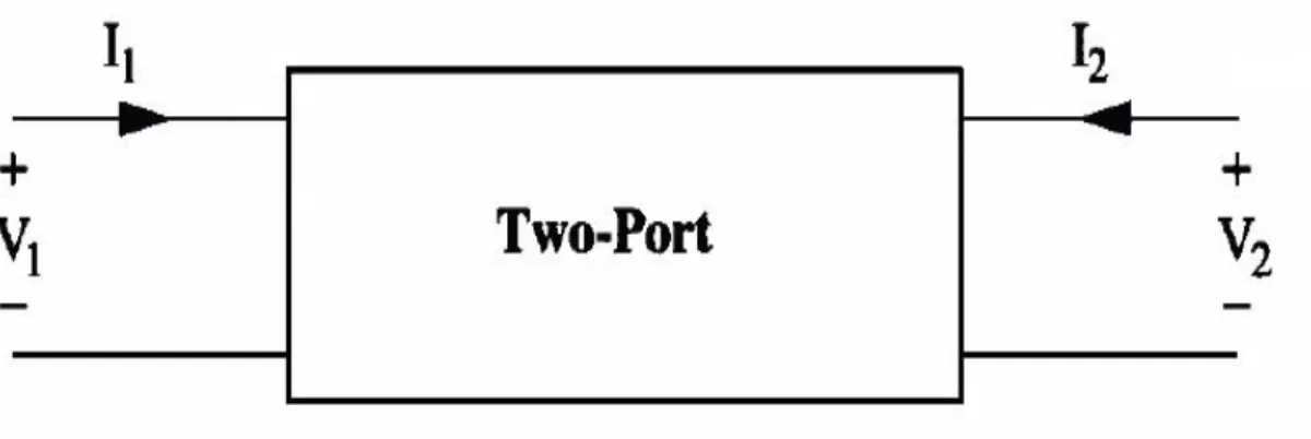
(41) the transmission line model (TLM) method [4-3]. The TLM pattern, as illustrated in Fig. 4.3, was designed in the process control monitor (PCM). In this particular approach, a linear array of contacts pad is fabricated with various spacing between them. The distances between TLM electrodes are 3 μm, 5 μm, 10 μm, 20 μm, and 36 μm, respectively. The resistance between the two adjacent electrodes can be plotted as a function of the space between electrodes and is expressed by the following equation R 2 RC RS L W. (4-11). ,where R is measured resistance, RC is contact resistance, RS is sheet resistance of channel region, W is electrode width, and L is the space between electrodes. As Fig. 4.4 shows, extrapolating the data to L=0, one can calculate a value for the term RC. And the specific contact resistance ρC can be further extracted by the following formula.. C . W 2R2 RS. (4-12). In general, the typical measured contact resistance for InGaAs QWFET was < 1 x 10⁻⁶ Ω-cm2.. 4.3 Scattering Parameters [4-2]. Field-effect transistor with the input and output terminals can be treated as a two-port network as shown in Fig. 4.5. Many characteristics such as gain, return loss and impedance matching can be calculated from relationship among the input and output signals. The impedance parameters (z-parameters), conductance parameters (y-parameters) and hybrid parameters (h-parameters) are used to characterize the devices. While the frequency is up to several GHz, the z-, y-, h- parameters can not be directly obtained by open or short circuits because of the reflected wave from the open or short terminations, which will induce the network oscillations. Therefore, the scattering parameters (S-parameters) are used to. 26.
(42) characterize the performance of a device at high frequency. Fig. 4.6 shows the equivalent two-port network schematic at high frequency. Generally, the Scattering parameters, which referred to as s-parameters, are fundamental to microwave measurement. S-parameters are a way of specifying return loss and insertion loss. The relation of the microwave signals and s-parameters are defined as follows: b s s-parameters: 1 11 b 2 s 21. s 12 a 1 * s 22 a 2 . (4-13). Microwave signals going into or coming out of the input port are labeled by a subscript 1. Signals going into or coming out of the output port are labeled by a subscript 2. The electric field of the microwave signal going into the component port is designated a; that leaving the port is designated b. Therefore, a1 is the electric field of the microwave signal entering the component input. b1 is the electric field of the microwave signal leaving the component input. a2 is the electric field of the microwave signal entering the component output. b2 is the electric field of the microwave signal leaving the component output. By definition, then,. s11 . b1 a1 a 2 0. s 21 . b2 a1 a 2 0. s12 . b1 a 2 a1 0. s 22 . b2 a 2 a1 0. (4-14). Consequently, s11 is the electric field leaving the input divided by the electric field entering the input, under the condition that no signal enters the output. Because b1 and a1 are. 27.
(43) electric fields, their ratio s11 is a reflection coefficient. Similarly, s21 is the electric field leaving the output divided by the electric field entering the input, when no signal enters the output. Therefore, s21 is a transmission coefficient and is related to the insertion loss or the gain of the device. s22 is similar to s11, but looks in the other direction into the device.. 4.4 Current-Gain Cutoff Frequency (fT) and Maximum Oscillation Frequency (fmax). Current-gain cutoff frequency (fT) is defined as the frequency at which the short-circuit current-gain becomes unity. The intrinsic s-parameters are extracted to determine the value of fT and which is determined by extrapolation of the short-circuit current gain h21 = 0 dB. Here h21 can be defined as h 21 . 2 s 21 (1 s11 )(1 s 22 ) s12 s 21. (4-15). fT can also be expressed by using circuit elements: fT . gm 2 (C gs C gd ). fT . gm Z v v w 1 G sat sat 2CG w Z G LG 2 2LG. (4-16). (4-17). The (Cgs + Cgd) is the total capacitance related to the schottky gate. From this relation, we could see that in order to achieve high fT, enhancing gm and decreasing total gate capacitance must be achieved. Because small total gate capacitance is accomplished by short gate length, and decreasing gate length can increase the electronic field under the gate and then accelerate the channel electron transport property. Therefore, the shrinking of gate length is an effective way to get high gm and low Cg so as to attain high fT. Another important parameter is fmax, which is the frequency where the power gain falls to unity. fmax is expressed as. 28.
(44) f max . fT R Ri Rs ( 2f T Rg C gd ) 2 g Rds . (4-18). 1 2. This expression shows that in order to obtain useful power gain at high frequency, the fT of a device must be large; in addition, the resistances of gate, source and drain must be small.. 4.5 Device Modeling Technique. When defining the high frequency RF performance of the QWFETs, it is essential to de-embed all the conductors which are on the top surface of the wafer such as the pad, metal, and interconnect. Detailed layout of the device in this study is shown in Fig. 4-7. In this study, an approach that combines the conventional way and 3-D full wave electromagnetic analysis is proposed and the intrinsic parameters of devices are extracted. To accurately determine the equivalent circuit model, the overall structure is divided into several blocks, including gate parasitic, drain parasitic, source parasitic and intrinsic part as shown in Fig. 4-8. The parasitic elements should be kept at fixed values and not scalable with device size. The intrinsic block could further be divided into different equivalent circuit elements and shown in Fig. 4-9. Standard gradient optimization routine is used to minimize the error function value, which is defined as the difference between the modeled and measured S-parameters. In order to rigorously determine the parasitic elements, CST Microwave Studio which is based on finite integration algorithm in time domain (FIT) is applied to analyze the structure. It is observed from the plot that the two source buses are held at a lower potential referenced to the gate and source pads thus the E-filed lines tend to terminate at these buses indicating a strong capacitive parasitic (Fig. 4-10 a). To illustrate the difference, a similar structure without the two source buses is simulated and the electric filed at 10 GHz is plotted in Fig. 4-10 b, where a much coarser electric field distribution between the gate (drain) pad. 29.
(45) and source region is observed. Based on the EM analysis of the structure, the strong capacitive parasitic behavior between the gate (drain) pad and the source buses suggests two additional capacitors to be included in the equivalent circuit.. 4.6 Noise Figure. NF can be well approximated by the semi-empirical equation given by Fukui [4-4] and is shown as the following equation: NF = 1+ k (f/fT) [gm (Rg+Rs)]1/2, = 1+ 2πkf (Cgs + Cgd) [gm (Rg+Rs)]1/2. (4-19). , where k is a fitting parameter. Generally, the reduction in Lg does not necessarily minimize the NFmin because Rg tends to increase due to a vertical resistance component of gate resistance, and also gm decreases due to a degraded gate drive so-called “short-channel effect”. Therefore, a reduction in Rg and suppression of the short-channel effect are necessary to minimize NFmin.. 30.
(46) Fig. 4.1 Band diagrams of QWFET at three different locations along the channel.. Eq. (4.4). Fig. 4.2 Drain current of III-V QWFETs predicted by Eq. (4-4).. 31.
(47) Fig. 4.3 TLM pattern.. Fig. 4.4 The illustration of utilizing TLM to measure ohmic contact resistance.. 32.
(48) Fig. 4.5 The equivalent two-port network schematic at low frequency.. Fig. 4.6 The equivalent two-port network schematic at high frequency.. 33.
(49) Fig. 4.7 The device layout used in this study.. 34.
(50) Gate. IN. Intrinsic. Parasitic. Parasitic. Zo,. Drain. Zo,. Source Gate-Sourc. Parasitic. Drain-Sourc e. e. GND Transmission line to accommodate for possible phase shift caused by probe positioning variation. Fig. 4.8 The block diagram with determined parasitic elements for the overall device structure.. IN. Zo,. Gate. Drain. Parasitic. Parasitic. Zo,. OUT. Source Gate-Source P. Parasitic. Drain-Source P. iti. iti. GND. Fig. 4.9 Functional blocks of the equivalent circuit model, divided according to the scalability with device size.. 35.
(51) (a). (b). Fig. 4.10 Analyzed electric field plot of the 2x50um device at 10 GHz. (a) with the source buses of the device (b) without the source buses of the device. 36.
(52) Chapter 5 Experimental results and discussions. 5.1 40 nm InAs-Channel Based QWFETs for High-Speed and Low-Voltage RF Applications by using Two-Step Recess and Pt Gate Sinking Processes 5.1.1 Introduction. For commercial and military applications of millimeter wave and sub-millimeter wave systems such as wireless LANs, outer-space radars, mobile communications and hand-held imagers etc., the key component of the systems is the front-end amplifier in the receiver. And the system sensitivity is ultimately determined by the performance of the front-end amplifiers which should possess outstanding high frequency features and low noise characteristics. In addition to the requirements of high gain and low noise, low DC power consumption is also in highly demand. Among all the possible technologies to meet such stringent requirements, high indium content InGaAs-based QWFETs are particularly promising. Because the InGaAs material own significant transport properties like high electron mobility, high saturation velocity, high sheet electron densities, and large Γ to L valley separation even in low electric field. Besides the excellent electrical properties of InGaAs material, the superior band-gap design of QWFETs also leads InxGa1-xAs QWFETs incomparable in high speed and low voltage performances. For devices operating in high frequency region, current-gain cutoff frequency (fT) is a significant index. fT is defined as the frequency which the current-gain becomes 0 dB. fT can also be expressed by using circuit elements as following: fT . gm 2 (C gs C gd ). 37.
(53) fT . gm Z v v w 1 G sat sat 2CG w Z G LG 2 2LG. As shown in the above relations, in order to achieve high fT, it is necessary to enhance gm and decrease total gate capacitance. In general, small total gate capacitance can be accomplished by shortening the gate length, and decreasing gate length can also increase the electronic field under the gate resulting in the accelerating of the transport property of the channel electrons. Therefore, shrinking the gate length is an effective way to get high gm and low Cg so as to attain high fT. For the noise performance, minimum noise figure (NFmin) can be well approximated by the semi-empirical equation given by Fukui [5-1] and is shown as the following equation: NFmin = 1+ k (f/fT) [gm (Rg+Rs)]1/2, = 1+ 2πkf (Cgs + Cgd) [ (Rg+Rs)/gm]1/2 , where k is a fitting parameter. It can be seen that the reduction of the parasitic capacitances and parasitic resistances are the keys to achieve low noise figure. And this can be accomplished by the shrinkage of gate length and the usage of low resistance structure layers and process. Although the reduction of gate length seems to be a good approach both for high frequency and low noise performance, such approach may generate the performance degradation caused by the short channel effect. Thus, care must be taken in obtaining the optimal performance without the short channel effect. Therefore, two-step recess process [5-2] and Pt gate sinking process were developed to solve this problem. Two-step recess process and Pt gate sinking technology have been widely used in the fabrication of QWFETs since they provide the promising solutions that enable vertical scaling shrinkage of gate-channel distance without increasing the access resistance. Meanwhile, the short-channel effect can be effectively minimized. By precise time control of the annealing time for Pt gate sinking process, Pt will diffuse toward channel. This reaction makes the gate electrode further close to channel layer, and it is beneficial for high frequency devices as well as for logic applications.. 38.
(54) Another advantage of using Pt-based structure is the relatively large schottky barrier height which will suppress gate leakage current. In this work, the electron beam lithography system was used to fabricate nanometer (40 nm) gate length for InAs QWFETs. Besides, two-step recess and Pt gate sinking processes were applied simultaneously to effectively reduce the gate-channel distance. The measured DC, RF and noise results will be presented here.. 5.1.2 Experiment. The QWFET structure in this study was grown by molecular beam epitaxy (MBE) on a 2-in diameter InP substrate, and the schematic structure is shown in Fig. 5.1.1. The structure layers from bottom to top consist of a 500 nm In0.52Al0.48As metamorphic buffer layer, a 5 nm InAs channel layer combining with a 3 nm In0.53Ga0.47As lower sub-channel layer and 2 nm In0.53Ga0.47As upper sub-channel layer, then, a 8 nm In0.52Al0.48As Schottky barrier layer with Si planar doping (4x1012cm-2), a 5 nm InP etching stop layer and a 40 nm highly Si-doped In0.53Ga0.47As cap layer (1×1019cm-3). The In0.53Ga0.47As sub-channels here were applied to enhance the electron confinement in the thin InAs layer and improve the electron transport properties [5-3]. For the device fabrication, the active area of the device was isolated by wet etching. Au-Ge-Ni-Au was deposited on heavily doped n-InGaAs cap layer and then alloyed in rapid thermal annealing (RTA) at 250℃ for 30 second to form source and drain ohmic contacts with low contact resistance and sheet resistance. Before the formation of T-shaped gate photoresist, the 600Å silicon nitride was deposited by plasma enhanced chemical vapor deposition (PECVD) as the support of the following 40nm gate foot. The T-shaped gate photoresist was carried out by using 50-kV JEOL electron beam lithography system (JBX 6000FS). The tri-layer EB photoresist system (ZEP/PMGI/ZEP) with double exposure and. 39.
(55) development was used to define the 40nm gate length. The top layer of T-shaped gate was exposed with low dosage, and the fine footprint was written with high dosage. Through anisotropic CF4 RIE dry etching, the gate foot was precisely replicated on 600Å SiNx layer. Then, the two-step recess technique was performed. The first step of recess was cap layer etching performed by using PH-adjusted solution of succinic (S.A.), NH4OH and H2O2. And the second step of recess etching was operated by inductive coupled plasma (ICP) with argon ambient to remove the InP etching stop layer under the gate. Schottky gate metal, which was composed of Pt(12nm) /Ti(80nm) /Pt(60nm) /Au(180nm), was then deposited by electron beam evaporation. Gate metal will form after lift-off procedure by acetone and ZDMAC. An adequate time of Pt sinking annealing at 250 ℃ was controlled to obtain the optimal performance for these devices. Finally, 100-nm-thick silicon nitride layer was deposited by PECVD at 200℃ for 10 min for devices passivation. SEM image of the 40-nm T-shaped gate is shown in Figure 5.1.2. As can be seen from SEM image, the fabricated 40-nm T-gate shows structural stability, even though the gate foot is narrow.. 5.1.3 Result and discussion. Fig. 5.1.3 and Fig. 5.1.4 show the DC I-V curves of the 40 nm InAs QWFETs with and without two-step recess and Pt gate sinking processes. Due to the high carrier concentration of the InAs/In0.53Ga0.47As composite channel material and the ultra low ohmic contact resistance of 0.02 Ω‧mm measured by TLM method, the 40nm InAs QWFETs exhibit high drain current density. Although the drain current 1050 mA/mm (VDS = 0.5 V, VGS = 0 V) of devices without two-step recess and gate sinking processes is higher than the device with these techniques of 390 mA/mm, the devices with these techniques exhibit much better pinch-off and current saturation characteristics compared to the devices without using these techniques.. 40.
數據

+7
相關文件
了⼀一個方案,用以尋找滿足 Calabi 方程的空 間,這些空間現在通稱為 Calabi-Yau 空間。.
A factorization method for reconstructing an impenetrable obstacle in a homogeneous medium (Helmholtz equation) using the spectral data of the far-field operator was developed
You are given the wavelength and total energy of a light pulse and asked to find the number of photons it
Reading Task 6: Genre Structure and Language Features. • Now let’s look at how language features (e.g. sentence patterns) are connected to the structure
• ‘ content teachers need to support support the learning of those parts of language knowledge that students are missing and that may be preventing them mastering the
volume suppressed mass: (TeV) 2 /M P ∼ 10 −4 eV → mm range can be experimentally tested for any number of extra dimensions - Light U(1) gauge bosons: no derivative couplings. =>
incapable to extract any quantities from QCD, nor to tackle the most interesting physics, namely, the spontaneously chiral symmetry breaking and the color confinement..
• Formation of massive primordial stars as origin of objects in the early universe. • Supernova explosions might be visible to the most
