390 IEEE ELECTRON DEVICE LETTERS, VOL. 33, NO. 3, MARCH 2012
Performance Enhancement of Thin-Film Transistors
With Suspended Poly-Si Nanowire Channels by
Embedding Silicon Nanocrystals in Gate Nitride
Chia-Hao Kuo, Horng-Chih Lin, Senior Member, IEEE, and Tiao-Yuan Huang, Fellow, IEEE
Abstract—In this letter, we fabricated and characterized
thin-film transistors with a suspended poly-Si nanowire (NW) channel and gate nitride with embedded silicon nanocrystals (Si NCs). The embedded Si NCs increase the surface roughness, thus reducing the adhesive force as the nitride is in contact with the poly-Si NW channel during the operation. Such a feature results in a reduction in pull-in voltage and sharper pull-out behavior. Moreover, this approach also greatly improves the endurance characteristics of the devices.
Index Terms—Adhesive force, nanocrystal (NC), nanowire
(NW), poly-Si.
I. INTRODUCTION
M
ICROELECTROMECHANICAL MOSFETs have re-cently drawn considerable attention and been widely studied because of their potential applications in several ar-eas, such as switches, resonators, memory, and sensor devices [1]–[7]. One important issue associated with most suspended-type devices is the high operation voltage (> 5 V), which makes it incompatible with nowadays CMOS design [1], [2], [6]. To overcome this hurdle, we have recently proposed a novel device with suspended poly-Si nanowire (NW) channels, which can effectively decrease the operation voltage by shrinking the air gap thickness down to the sub-100-nm regime [8]. This allows the pull-in of the suspended channel to occur at a gate voltage smaller than 2 V. Moreover, owing to the tiny NW channels, the ratio between the etch depth and thickness of the sacrificial oxide is significantly reduced, allowing the use of a simple wet chemical etch step to release the suspended object. Nevertheless, we have also found that the endurance of the fabricated devices is only mediocre. That is, significant shrinkage in the window between the two logic states is usually observed within a few hundreds of cycles. To address this issue,Manuscript received October 5, 2011; revised November 21, 2011; accepted December 3, 2011. Date of publication January 23, 2012; date of current version February 23, 2012. This work was supported in part by the National Science Council of the Republic of China under Contract NSC 99-2221-E-009 -172 and Contract NSC 99-2221-99-2221-E-009 -167 -MY3. The review of this letter was arranged by Editor A. Nathan.
C.-H. Kuo and T.-Y. Huang are with the Department of Electronics Engi-neering and Institute of Electronics, National Chiao Tung University, Hsinchu 300, Taiwan.
H.-C. Lin is with the Department of Electronics Engineering and Institute of Electronics, National Chiao Tung University, Hsinchu 300, Taiwan, and also with the National Nano Device Laboratories, Hsinchu 300, Taiwan (e-mail: [email protected]).
Color versions of one or more of the figures in this letter are available online at http://ieeexplore.ieee.org.
Digital Object Identifier 10.1109/LED.2011.2179515
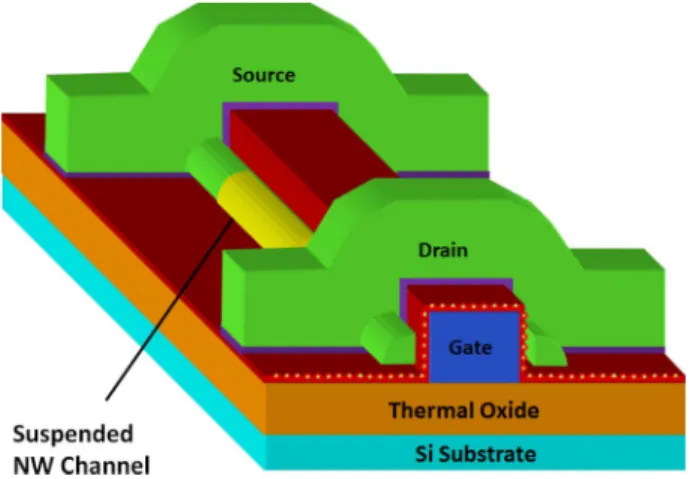
Fig. 1. Schematic structure of the device with Si NCs embedded in the gate nitride.
in this letter, we present an improved version by incorporating silicon nanocrystals (Si NCs) in the gate nitride layer of the suspended NW channel.
II. DEVICESTRUCTURE ANDFABRICATION
Fig. 1 depicts the schematic structure of the device with Si NCs incorporated. The fabrication process of the device is basically the same as that described in [8] and [9]. In brief, after the formation of an n+ poly-Si gate on a Si wafer capped with a thermal oxide, SiN (20 nm), sacrificial oxide (40 nm), and poly-Si (100 nm) were subsequently deposited. Afterward, source/drain (S/D) regions were lithographically defined, whereas poly-Si NW channels were defined by using the sidewall spacer etching techniques [10]. To suspend the NW channels, the sacrificial oxide between the NW and the gate nitride was then selectively removed with an HF-containing so-lution. In this letter, the Si NCs incorporation was done with the following procedure conducted in a low-pressure chemical va-por deposition system at 700◦C [11]. First, a 15-nm-thick bot-tom SiN was deposited with dichlorosilane (SiCl2H2, 65 sccm) and ammonia (NH3, 15 sccm) gases. Subsequently, by turning off the NH3 gas flow and increasing the flow rate of the dichlorosilane to 100 sccm, Si NCs are in situ formed on the surface of the deposited nitride. The duration of this period is 45 s. Finally, a 5-nm-thick top-SiN with a flow rate condition identical to that of the bottom one was deposited to cover the Si NCs. For comparison purposes, control devices with a single 20-nm-thick SiN layer were also fabricated.
KUO et al.: THIN-FILM TRANSISTORS WITH SUSPENDED POLY-SI NANOWIRE CHANNELS 391
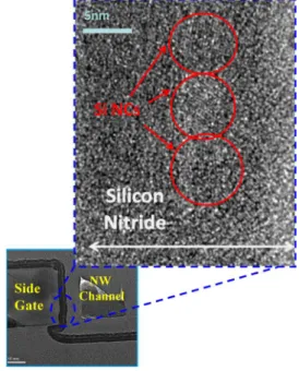
Fig. 2. Cross-sectional schematics of devices (a) with and (b) without Si NCs embedded in the nitride film and AFM images of blanket nitride films (c) with and (d) without Si NC dots incorporated (1 μm× 1 μm scan size).
Fig. 3. Cross-sectional TEM picture of a device with Si NCs. The picture was taken before the sacrificial oxide was removed. Inset shows an enlarged view of the Si NCs in the silicon nitride.
The cross-sectional views of the fabricated devices with and without embedded Si NCs in the SiN layer are shown in Fig. 2(a) and (b), respectively. Fig. 2(c) and (d) displays the atomic force microscopic (AFM) images (1× 1 μm2) taken from blanket SiN films with and without embedded Si NCs, respectively. The root-mean-square roughness values of the SiN films with and without embedded Si NCs were 0.703 and 0.234 nm, respectively. The density of Si NC dots in Fig. 2(c) is es-timated to be around 5× 1011cm−2. Fig. 3 displays the
cross-Fig. 4. Hysteresis I–V characteristics of the fabricated devices with and without embedded Si NCs.
sectional transmission electron microscopic (TEM) image of a fabricated device taken prior to the stripping of the sacrificial oxide layer. In the picture, the embedded Si NCs in the SiN are clearly observed.
III. RESULTS ANDDISCUSSION
Typical hysteresis characteristics of devices with and without embedded Si NCs are shown in Fig. 4. It is shown in the figure that the turn-on of the device can be triggered at a much smaller gate voltage (VG) as Si NCs are incorporated. As mentioned in
the previous section, the presence of the Si NCs roughens the nitride surface, and the electric field strength near the protrud-ing nitride surface is enhanced durprotrud-ing operation. Such feature may increase the effective electrostatic force between the gate
392 IEEE ELECTRON DEVICE LETTERS, VOL. 33, NO. 3, MARCH 2012
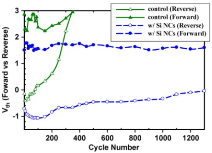
Fig. 5. Endurance characteristics of devices with and without embedded Si NCs.
and the channel at a specific VG, explaining the experimental
observation.
In addition, for the control device, it is shown in Fig. 4 that the subthreshold characteristics of the forward sweeping curve is much steeper than the reverse one. This effect can be explained by the presence of an additional adhesive force while the channels are in intimate contact with the gate nitride, which would retard the detachment of suspended NWs from the gate nitride [12]. On the other hand, the device with Si NCs exhibits a sudden drop in the reverse sweeping with subthreshold swing (SS) of∼49 mV/dec. This is again attributed to its roughened gate nitride surface. As the gate voltage is swept backward to release the electrically attractive force between the two objects, the adhesive force existing in the contact portion of the gate nitride and the NW channel would become the dominant component to balance the restoring force coming from the displacement of the NW channels [13]. For nitride with Si NCs incorporated, the increased surface roughness reduces the effec-tive contact area between the nitride and the suspended channel and thus the associated adhesive force. As a consequence, the pull-off action of the suspended NW channels can be triggered earlier than the control sample and results in a steeper SS.
Another important advantage offered by the proposed embedded-Si-NCs approach is the improvement of device re-liability. Fig. 5 shows the measured endurance characteristics of devices with and without embedded Si NCs. For simplicity,
Vth is defined as VG@ID= 10 nA× (W/L). The cycling
tests were executed with cycles of consecutive forward and reverse sweeping measurements. In the figure, Vth values of both forward and reverse sweeping curves are recorded, and the difference between the two states is defined as the window size. It can be seen that, for the control device, the failure in terms of window shrinkage occurs after roughly 250 cycles. The failure mechanism is postulated to be related to the stiction or the contact fatigue of NWs [14]. On the other hand, considerable window size remains for the device with embedded Si NCs even after 1300 cycles. As the occurrence of stiction is closely related to the adhesive force between the contacted objects [13], [14],
obviously, the reduced effective contact area of the roughened nitride surface with the aforementioned NCs also benefits the endurance characteristics of the device operation.
IV. CONCLUSION
In this letter, we have refined a recently developed fabrication process by incorporating Si NCs in the gate nitride layer of the device with suspended poly-Si NW channels. With this refinement, significant performance improvements in terms of reduced turn-on voltage and meliorated endurance characteris-tics are demonstrated. These improvements are believed to be related to the roughened surface of the nitride with embedded Si NCs.
REFERENCES
[1] N. Abele, R. Fritschi, K. Boucart, F. Casset, P. Ancey, and A. Ionescu, “Suspended-gate MOSFET: Bringing new MEMS functionality into solid-state MOS transistor,” in IEDM Tech. Dig., 2005, pp. 479–481. [2] B. Pruvost, H. Mizuta, and S. Oda, “3-D design and analysis of functional
NEMS-gate MOSFETs and SETs,” IEEE Trans. Nanotechnol., vol. 6, no. 2, pp. 218–224, Mar. 2007.
[3] M. M. Agarwal, K. K. Park, R. N. Candler, B. Kim, M. A. Hopcroft, S. A. Chandorkar, C. M. Jha, R. Melamud, T. W. Kenny, and B. Murmann, “Nonlinear characterization of electrostatic MEMS resonators,” in Proc. IEEE Freq. Control Symp. Expo., Miami, FL, Jun. 4–7, 2006, pp. 209–212.
[4] N. Abele, A. Villaret, A. Gangadharaiah, C. Gabioud, P. Ancey, and A. Ionescu, “1T MEMS memory based on suspended gate MOSFET,” in IEDM Tech. Dig., 2006, pp. 1–4.
[5] H. M. Kotb, A. C. Salaün, F. Bendriaa, F. L. Bihan, T. M. Brahim, and J. R. Morante, “Sensing sensibility of surface micromachined suspended gate polysilicon thin film transistors,” Sens. Actuators B, Chem., vol. 118, no. 1/2, pp. 243–248, Oct. 2006.
[6] M. G. Bardon, H. P. Neves, R. Puers, and C. Van Hoof, “Scaling the suspended-gate FET: Impact of dielectric charging and roughness,” IEEE Trans. Electron Devices, vol. 57, no. 4, pp. 804–813, Apr. 2010. [7] K. Akarvardar, C Eggimann, D. Tsamados, Y. S. Chauhan, G. C. Wan,
A. M. Ionescu, R. T. Howe, and H. S. P. Wong, “Analytical modeling of the suspended-gate FET and design insights for low-power logic,” IEEE Trans. Electron Devices, vol. 55, no. 1, pp. 48–59, Jan. 2008.
[8] H. C. Lin, C. H. Kuo, G. J. Li, C. J. Su, and T. Y. Huang, “Operation of a novel device with suspended nanowire channels,” IEEE Electron Device Lett., vol. 31, no. 5, pp. 384–386, May 2010.
[9] C. H. Kuo, C. W. Hsu, H. H. Hsu, H. C. Lin, and T. Y. Huang, “Impacts of gap thickness scaling on thin-film transistors with suspended nanowire channels,” in Proc. IEEE Int. Symp. VLSI-TSA, Apr. 2011, pp. 1–2. [10] H. C. Lin, M. H. Lee, C. J. Su, T. Y. Huang, C. C. Lee, and Y. S. Yang, “A
simple and low-cost method to fabrication TFTs with poly-Si nanowire channel,” IEEE Electron Device Lett., vol. 26, no. 9, pp. 643–645, Sep. 2005.
[11] C. W. Luo, H. C. Lin, K. H. Lee, W. C. Chen, H. H. Hsu, and T. Y. Huang, “Impacts of nanocrystal location on the operation of trap-layer-engineered poly-Si nanowire gate-all-around SONOS memory devices,” IEEE Trans. Electron Devices, vol. 58, no. 7, pp. 1879–1885, Jul. 2011.
[12] W. W. Jang, J. B. Yoon, M. S. Kim, J. M. Lee, S. M. Kim, E. J. Yoon, K. H. Cho, S. Y. Lee, I. H. Choi, D. W. Kim, and D. Park, “NEMS switch with 30 nm-thick beam and 20 nm-thick high air gap for high density non-volatile memory applications,” Solid State Electron., vol. 52, no. 10, pp. 1578–1583, Oct. 2008.
[13] W. M. Van Spengen, R. Puers, and I. De Wolf, “On the physics of stiction and its impact on the reliability of microstructures,” J. Adhesion Sci. Technol., vol. 17, no. 4, pp. 563–582, 2003.
[14] G. De Pasquale, A. Somà, and A. Ballestra, “Mechanical fatigue analysis of gold microbeams for RF-MEMS applications by pull-in voltage mon-itoring,” Analog Integr. Circuits Signal Process., vol. 61, no. 3, pp. 215– 222, Dec. 2009.